Note : Les descriptions sont présentées dans la langue officielle dans laquelle elles ont été soumises.
l~G3~0
-1- RCA 81,676
FREQUENCY CONTROLLED RESONANT REGULATOR
This invention relates to switching regulator
power supplies.
Switched mode power supplies may be used to
generate supply voltages from an unregulated input
voltage. The power supply may include a switching stage
coupled to the primary winding of a power transformer for
generating output voltages across secondary windings of
the transformer. To regulate the output voltages, it is
known to pulse-width modulate the switching stage of, for
example, a flyback converter type of switched mode power
supply.
It is desirable to operate a switching power
supply at relatively high fre~uencies, such as between
50~150 kilohertz, to reduce the size of the associated
magnetic components such as the power transformer. At
these relatively high frequencies, pulse-width modulating
systems have several disadvantages. Electromagnetic
interference radiation is increased. Efficiency is
reduced due to the increased switching losses. Both of
these undesirable aspects result from the large number of
harmonics generated by a square wave output. Additionally,
in flyback converter types of switching regulators, a
relatively large peak reverse voltage stress is applied to
the secondary winding output rectifiers. Such peak
reverse voltage stress is undesirable for switching power
supplies operating at high fre~lencies and providing high
current from low voltage secondary supplies. Such
switching power supplies often use Schottky output
rectifiers which cannot sustain large peak reverse voltage
stresses.
To avoid the disadvantages of pulse width
modulators at high operating frequencies, sinewave
resonant power converters have been used. In such
converters, the power transformer includes relatively
tightly coupled primary and secondary windings. A
discrete inductor is placed in series with the primary
winding and a resonating capacitor is coupled across the
~2~ 0
-2- RCA 81,676
secondary winding. The resonating capacitor tunes
essentially with the discrete inductor to form a tuned
circuit that produces a generally sinewave output voltage
across the secondary winding. The amplitude of the output
voltage is determined by the operating frequency of the
voltage generator coupled to the primary winding and
discrete inductor. To provide regulation, the amplitude
of the output voltage is sensed and fed back to the
voltage generator to vary the generatorls operating
frequency.
A feature of the invention is a frequency
controlled resonant regulator that incorporates into the
power transformer the inductive portion of the regulator
tuned circuit. A first winding of a power transformer is
coupled to a source of unregulated voltage and to output
switching means. A controllable source of switching
signals is coupled to the output switching means for
operating the switching means at a controllable frequency
to generate a first alternating output voltage across a
second winding of the power transformer. The power
transformer incorporates substantial leakage inductance
between the two windings. A resonating capacitance is
coupled to the second winding for forming a tuned circuit
with the inductance of the transformer. The amplitude of
the output voltage is varied by varying the operating
frequency of the switching means. A sense signal is
coupled to the controllable source for developing a
control signal that varies the output frequency to provide
regulation of the output voltage.
In accordance with an aspect of the invention,
the inductance of the tuned circuit is obtained primarily
or exclusively from the leakage inductance of the power
transformer. No other inductance, such as a discrete
inductor, provides any significant inductance to the
tuning of the resonant circuit. Because such an
arrangement eliminates the need for a discrete inductor,
the power transformer construction is simplified, since
~Z637~Q~
-3- RCA 81,676
tight coupling of primary and secon~ary windings is not
required, resulting in substantial economies.
The output voltage verses frequency
characteristic of the tuned circuit is a function of
operating fre~uency. The output voltage of the tuned
circuit is greatly reduced at operating frequencies that
are much higher than the resonant frequency of the tuned
circuit. In carrying out the invention, the output
voltage verses frequency characteristic of the tuned
circuit may be advantageously used to provide standby or
auxiliary voltages that are available even when the main
regulated output voltages have been removed. Because the
inventive resonant regulator incorporates a high leakage
transformer, an auxiliary winding may be provided that is
tightly coupled to the primary winding but loosely coupled
to the regulated secondary winding that is being tuned by
the resonanting capacitor. To place the power supply in
standby mode of operation, the operating frequency of the
voltage generator is increased to a value that places the
operating point of the tuned circuit well above resonance.
The sinewave output voltage is effectively reduced to
insignificant value. However, because the auxiliary
winding is tightly coupled to the primary winding the
square wave auxiliary voltage that this winding supplies
is largely unaffected by the increase in operating
frequency. This auxiliary voltage may then be used as a
source of standby voltage.
In the Drawing:
FIGURE 1 illustrates a frequency controlled
resonant regulatorJ embodying the invention;
FIGURE 2 illustrates an electrical equivalent
circuit of the resonant power transformer of FIGURE l;
FIGURE 3 illustrates a family of curves of
output voltage verses frequency for the circuit of FIGURE
2;
FIGURE 4 illustrates another frequency
controlled resonant regulator, embodying the invention,
lZ~37C~10
-4- RCA 81,676
used as the power supply for a remote responsive
television receiver;
FIGURE 5 illustrates, in exploded perspective
view, a pot core that may be advantageously used in the
power transformers of FIGURES l and 4;
FIGURE 6 illustrates a side elevation view of a
pot core transformer including windings that may be
advantageously used as the power transformers of FIGURES 1
and 4; and
FIGURE 7 illustrates a cross-sectional view of
the transformer of FIGURE 6 viewed through the
cross-sectional lines 7-7.
The circuit of FIGURE l for drawing clarity is
separated into Part A and Part B, with transformer T4 and
capacitor Cr being shown in both parts.
A resonant regulator 20, embodying the
invention, illustrated in FIGURE l, includes a high
leakage transformer T4 having a primary winding W1 coupled
to an output switching stage 30 that includes an upper
switching device Sl comprising an output switching field
effect transistor Q6, paralleled by an oppositely poled
diode D5, and that includes a lower switching device S2
comprising an output switching field effect transistor Q7,
paralleled by an oppositely poled diode D6. An
unregulated DC voltage source 70 is coupled to primary
winding Wl and output switching transistors Q6 and Q7.
Unregulated voltage source 70 comprises a source
of alternating current, mains supply voltage 21 coupled
between input terminals 23 and 24 of a full wave bridge
rectifier 27 via an on-off switch 22 and a current
limiting resistor Rl. An unregulated direct voltage is
developed between output terminal 25 of bridge rectifier
27 and a current return terminal 26 designated as an earth
ground 40, no-t conductively isolated from mains source 21.
Filtering of the unregulated direct voltage is provided by
the series coupled capacitors C5 and C6 coupled between
bridge output terminal 25 and earth ground 40.
~2637Q~
-5- RCA 81,676
~ ridge output terminal 25 is coupled to upper
switching device S1; lower switching device S2 is coupled
to earth ground terminal 40. The upper terminal of primary
winding W1 of transformer T4 is coupled to terminal 28,
the junction of capacitors C5 and C6, and the lower
terminal of winding Wl is coupled through a DC blocking
capacitor C10 to switch output terminal 31, at the
junction of switches S1 and S2.
The connection of primary winding W1 to the
junction of capacitor C5 and C6 enables positive and
negative supply voltayes +Vin and -Vin to be alternately
applied across the winding during alternate conduction of
switches S1 and S2. By providing both polarity input
voltages, ~Vin, a single primary winding, without center
tap, ma~ be used, reducing the reverse voltage stresses on
semiconductor switches S1 and S2.
The development of voltages of both polarities
by means of bridge rectifier Z7 and capacitors C5 and C6
enables resonant regulator 20 to be connected to two
different AC main voltage levels. For example, when the
AC mains voltage is 220 VAC, the full wave bridge
rectifier arrangement described previously is provided.
When the AC mains supply voltage is at a lower voltage
level such as 120 VAC, then a jumper wire 2g is used to
connect terminal 28 directly to AC mains source 21 at
bridge input terminal 24. When jumper wire 29 is in use,
the rectifier diodes form a half-bridge, voltage doubler, to
develop substantially the same dual polarity voltages,
~Vin developed across respective capacitors C5 and C6
as are developed when a 220 VAC mains voltage source is
connected to bridge rectifier 27.
To control the frequency of operation of output
switches Sl and S2 of controllable output switching stage
30, a voltage controlled oscillator 50 generates a high
frequency, 50% duty cycle switching signal 32
illustratively at a nominal frequency f=fo~64 kilohertz.
Switching signal 32 is coupled to the bases of cpposite
conductivity signal transistors Ql and Q2, to alternately
.
~2~i37~3
-6- RCA 81,676
switch conduction between the two transistors. The
alternate switching of transistors Ql and Q2 produces
square wave voltages across windings W1 and W2 of a
coupling transformer T2. The square wave voltages across
windings W1 and W2 are 180 degrees out of phase with each
other, when each voltaye is referenced relative to the
respective undotted terminals of their windings. The
square wave voltages across windings W1 and W2 are
transformer coupled to windings W3 and W4 of transformer
T2 to produce the alternate switching into conduction of
turnoff transistors Q4 and Q5. The collector electrodes
of transistors Q4 and Q5 are coupled to the respective
gate electrodes of output switching transistors Q6 and Q7.
During the controlled switching of output
switches Sl and S2 by the switching signals 32 generated
in VCo 50, the alternate turnoff of output switching
transistors Q6 and Q7 is provided by the alternate
conduction of transistors Q4 and Q5. Assume for example
the top output switch S1 is conducting. The unregulated
voltage ~in developed across capacitor C5 is applied by
switch S1 to primary winding Wl of power transformer T~,
with the lower, dotted terminal of the winding being the
positive terminal. Forward gate drive voltage for output
switching transistor Q6 is supplied from winding Wb of a
driver transformer T3 that has a primary winding Wa
coupled to a feedback winding W3 of power transformer T4.
To turn off switch Sl, the square wave voltage
across winding W3 of transformer T2 turns on transistor Q4
and the oppositely phased square wave voltage across
winding W4 turns off transistor Q5. With transistor Q4
conducting, forward gate voltage for output switching
transistor Q6 is removed, turning off transistor Q6.
With transistor Q6 cut off, an opposite polarity
voltage is induced across primary winding W1 of
transformer T4 making the upper, undotted terminals of
primary winding Wl and feedback winding W3 of transformer
T4 positive. With a reversal in polarity across winding
Wl of transformer T4, diode D6 of switch S2 becomes
~Zfi3~QO
-7- RCA 81,676
conductive, taking up current in winding W1. The voltage
-Vin developed across capacitor C6 is applied to primary
winding Wl of transformer T4. The reversal in polarity
across winding W3 of transformer T4 is coupled via winding
Wa of transformer T3 to make the upper, undotted terminal
of secondary winding Wc of transformer T3 positive,
providing forward drive for output switching transistor
Q7. Later in the interval, when current in winding Wl
reverses in direction, conduction of the current transfers
from diode D6 to transistor Q7.
In this manner, voltage controlled oscillator
50, in combination with output switching stage 30,
comprise a voltage generator 80 that develops a 50% duty
cycle square wave input voltage that is applied to primary
winding W1 of resonant power trans~ormer T4. The
frequency of operation of voltage generator 80 is
controlled by the operating fre~uency f of voltage
controlled oscillator 50.
Power transformer T4 is constructed as a high
leakage inductance transformer with the primary side
windings Wl - W3 being relatively tightly coupled to one
another and with the secondary side windings W4 - W7 also
being tightly coupled to one another but loosely coupled
to the primary side windings. The operation of output
switching stage 30 generates a square wave alternating
polarity voltage across primary winding Wl to develop
alternating polarity voltages across primary side windings
W2 and W3 and secondary side windings W4 - W7.
The secondary side windings provide rectified
and filtered DC supply voltages +V0, +Vl, +V2 and -V3,
that are referenced to a chassis ground 60 that is
conductively isolated from earth ground 40. When resonant
regulator 20 is used as a power supply for a video display
monitor or television receiver, the secondary side DC
supply voltages provide power to such loads as the
horizontal deflection and high voltage circuits, powered
by the +V0 DC supply, the vertical deflection circuit,
12G370~3
-8- RCA 81,676
powered by the +V1 DC supply, and the small signal
circuitry, powered by the +V2 and -V3 DC supplies.
To regulate the secondary side output voltages
against loading changes and against changes in the
unregulated voltage developed at bridge rectifier output
terminal 25, a resonanting or tuning capacitor Cr is
coupled across one of the secondary side windings,
illustratively across secondary side winding W7.
Resonanting capacitor Cr forms a series tuned circuit 10
with the leakage inductance of power transformer T4 to
produce generally sinusoidal alternating output voltages
across all the tightly coupled secondary side windings.
The amplitude of each of the alternating output voltages
i s es tablished in accordance with the controllable
frequency of operation of voltage generator 80.
FIGURE 2 illustrates a simplified electrical
e~uivalent circuit of high leakage inductance power
transformer T4 referred to the primary side and of the
resonanting capacitor reflected to the primary side as the
capacitance C'r. The inductance of transformer T4 may be
represented as a T-network comprising series inductors Ll
and L2, and a shunt inductor L coupled to the junction of
inductors Ll and L2. When a source of alternating input
voltage Vin is applied to the electrical equivalent
circuit of FI~URE 2, an alternating output voltage VOUt is
developed across capacitor Clr and across a load impedance
RL, where RL represents the equivalent load impedance,
reflected to the primary side, of the load circuits
coupled to the secondary side windings W4 - W7. The
impedance Rs represents the source impedance of the
voltage source Vin and the winding resistances of
transformer T4.
Assume for simplified explanatory purposes that
the input voltage Vin is a sinewave voltage`of amplitude
Vi for producing a sinewave output voltage VOUt of a
nominal amplitude V0 across a resistive load impedance RL
=RLo for some nominal operating state of the power supply.
~6~ 0
-9- RCA 81,676
R~sonanting capacitor Clr forms a series tuned
circuit with the T-network inductance (L, Ll and L2), of
the electrical equivalent circuit of transformer T4 in
FIGURE 2. FIGURE 3 illustrates the output voltage
characteristic ~=VOUt/Vo in decibels as a function of
operating frequency f, for the electrical equivalent
circuit of transformer T4 in FIGURE 2. As illustrated by
the family of curves in FIGURE 3, tuned circuit 10 of
FIGURE 2 has a resonant frequency fL that varies slightly
as a function of loading, with the resonant frequency
increasing as the loading decreases. For example, the
resonant frequency fLl , associated with a load resistance
RL1 is slightly greatex than the resonant frequency fL3
associated with a smaller load resistor RL3.
The voltage gain ~, or equivalently, the
amplitude of the output voltage VOUt, depends on the
operating characteristics of the transformer power supply
electrical equivalent circuit of FIGURE 2, including the
operating frequency f of the voltage Vin. For the nominal
operating characteristics of, for example, Vin=Vi and
RL=RLo~ the output voltage VOUt =V0 at a nominal operating
frequency of f=fO. The transformer and tuned circuit
operating point, given these characteristic values, is
located at point P0 of curve 23 in FIGURE 3.
To regulate the amplitude of the output voltage
VOUt against changes in the load RL and against changes in
the amplitude of the input voltage Vin, the operating
point of tuned circuit 10 is changed by varying the
operating frequency f. For example, assume a decrease in
loading from a load resistance RLo to RLl. If the
operating frequency remains unchanged at f=fO, then the
operating point of tuned circuit 10 of FIGURE 2 changes
from point P0 of curve 123 in FIGURE 3 to the operating
point Pl of curve 122, thereby producing an undesirable
increase in output voltage amplitude. To maintain a
constant output voltage amplitude when the loadiny
decreases, the operating frequency is decreased from the
frequency fO to the lower frequency fOl The new
~L2~37~0
-10- RCA 81,676
operating point is moved to the point Po1 of curve 122,
keeping the amplitude of the output voltage unchanged.
In a similar manner, the operating frequency f
is varied when the input voltage 'Vin changes in amplitude.
Curve 121 of FIGURE 3 illustrates the voltage gain ~
verses frequency f of the transformer power supply of
FIGURE 2 for a load RL=RLl and for an input voltage Vin=
Vi'that is greater than the voltage Vi associated with
curve 122. Thus, to maintain a constant amplitude output
voltage, the operating frequency of tuned circuit 10 is
decreased from the frequency fOl to the frequency fo2 to
move the operating point from Pol to -the operating point
Po2 having the same output voltage amplitude.
In resonant regulator 20 of FIGURE 1 the
operating point of the tuned circuit of transformer T4 is
changed to maintain relatively constant secondary side DC
supply voltages with changes in unregulated input voltage
and with changes in loading by the secondary side load
circuits. In FIGURE 1, a sense voltage Vf representative
of the regulated DC output voltage +V0, for example, is
developed at the junction of voltage dividing resistor R34
and R35, of a regulator control circuit 55. The voltage
Vf is coupled to the inverting input terminal of a
comparator U4B. The non-inverting input terminal of
comparator U4B is grounded. To provide a reference
potential for comparator U4B when the non-inverting input
terminal is grounded, a negative bias voltage developed
across zener diode Z3 is summed with the feedback voltage
Vf at the inverting input terminal of comparator U4B.
The error voltage output Ve of comparator U4B is
amplified by amplifier U4A, lowpass filtered by an RC
network comprising resistor R22 and capacitor C18 and
applied as a control voltage Vc to control the operating
frequency f of voltage controlled oscillator 50 and
voltage generator 80. The biasing of comparator U4A is
such that under nominal conditions, a zero error voltage
Ve produces an operating frequency fO for VC0 50.
~Z637QO
~ RC~ 81,676
As the DC output supply voltage +V0 tends to
decrease, for example, due to either increased loading or
decreased unregulated input voltage, the control voltage
Vc increases, to increase the operating frequency f of VCO
50 and voltage generator 80. The operating point of tuned
circuit 10 is moved to the right in the voltage gain
verses frequency illustration of FIGU~E 3, to maintain a
constant output voltage.
In accordance with a feature of the invention,
resonant regulator 20 includes overload protection that is
automatically provided by the frequency control circuitry
of the regulator. Because resonant power transformer T4
is designed as a series resonant tuned circuit, the
resonant output voltages decrease rapidly as the operating
frequency f becomes significantly greater than the
resonant frequency fL of the tuned circuit. Consider an
overcurrent operating condition where, for example,
picture tube arcing results in a short circuit to ground
of the final anode electrode. Overload current is then
drawn from the +V0 DC supply terminal, causing the supply
voltage +V0 to decrease. For a decrease iIl output voltage
+VO, regulator control circuit 55 is designed to increase
the frequency of operation f of VCO 50 moving the
operating point of tuned circuit 10 to the right.
However, under overload conditions the load resistance RL
is substantially decreased resulting in the operating
curve changing from a curve such as curve 123 of FIGURE 3
to a curve such as curve 125, having decreased maximum
output voltage amplitude, substantially below the
amplitude of the output voltage V0 at the nominal
operating point P0.
Because of this tuned circuit response
characteristic of the voltage gain curve under an overload
condition, regulator control circuit 55 drives the
operating frequency f beyond the resonant fre~uency fL4 f
curve 125 in Fl&URE 3, in an attempt to overcome the
decrease in output voltage ~V0. Once the operating
frequency is driven above resonance, the output voltage
~6t~7Q~
-12- RCA 81,676
decreases rapidly as a function of increasing frequency f
above the resonance point. Regulator control circuit 55
continues to drive the operating frequency higher until
the ma~imum frequency fmax is reached. At this point,the
extreme range of frequency operation of resonant control
circuit 55 is reached, and the operating frequency of
voltage generator 80 is kept at this frequency. One notes
that at the overload operating frequency fmax~ the output
voltage VOUt is substantially below its nominal voltage
V0, decreasing by over 20 decibels in the illustration of
FIGURE 3.
The frequency limit fmax for overload operation
is established by diodes D12 and D18 of FIGURE 1 that are
coupled between inverting input terminal 7 and output
terminal 11 of comparator U4B. When the feedback voltage
Vf decreases substantially under overload conditions, the
diodes D12 and D18 become forward biased to clamp the
error voltage Ve of comparator U4B to the voltage at the
inverting terminal 7. This prevents the error voltage Ve
and the operating frequency f from increasing by any
further significant amount.
The automatic, high frequency overload type of
operation that resonant regulator 20 assumes is
advantageously produced by designing the regulator so that
the operating point of tuned circuit 10 under normal
voltage and load conditions is at a point below resonance
in the family of operating curves of FIGURE 3. By
designing the operating points to be below resonance,
under normal operation, regulator control circuit 55 must
drive the operating frequency to the right, to higher
frequencies, for increased loading. Thus, when an
overload conditions occurs, the operating frequency is
driven to the right beyond the resonance frequency, and by
means of a positive feedback type of effect, continues to
be driven to the right until the overload limit frequency
fmax is reached.
Additionally, a diode D13 is provided that
limits the lowest frequency of operation fmin to which
~2G37~6~
-13- RCA 81,676
regulator control circuit 55 is capable of driving VCO 50.
Diode D13 is poled in a direction opposite to diode D12,
with the anode of diode Dl3 coupled to inverting input
terminal 7 of comparator U4B, and the cathode of the diode
coupled to output terminal 11. If during start-up or
during a fault operating condition the voltage at
inverting terminal 7 of comparator U4B increases greatly,
the error voltage Ve at output terminal 11 of comparator
U4B decreases sufficiently to forward bias diode D13.
When diode D13 conducts, no further significant decrease
in error voltage Ve and operating frequency f can occur.
~he minimum operating frequency fmin is selected so as to
keep currents in output switches S1 and S2 and in pri~ary
winding W1 of transformer T4 to safe levels.
In accordance with another feature of the
invention, ~y providing the resonant inductance for tuned
circuit 10 prlmarily or exclusively as the inductance in a
high leakage transformer, auxiliary windings, tightly
coupled to primary winding W1, such as auxiliary winding
W2, are capable of developing output voltages even when no
significant voltages are being developed by the secondary
side windings W4-W7. Provided that voltage generator ~0
is operating to produce a s~uare wave voltage across
primary winding W1, an auxiliary sguare wave voltage is
also developed across winding W2 having a frequency that
is determined by the frequency of operation of generator
80. The amplitude of the auxiliary secondary winding
voltage is not significantly affected by the fre~uency of
operation of generator 80, nor by the operating point of
tuned circuit 10. The amplitude of the auxiliary supply
voltage is however unregulated and varies with changes in
the amplitude of the unregulated voltage developed at
bridge rectifier output terminal 25.
~he square wave voltage across auxiliary winding
W2 is rectified by a diode D9, filtered by a capac~tor
C11, and regulated by a zener diode Z1 to generate a
regulated, positive auxiliary supply voltage +V~s. In a
similar manner, a regulated negative auxiliary supply
~Z637Q~
-14- RCA 81,676
voltage -Vss is developed from the auxiliary square wave
voltage developed across winding W2 by means of
rectification ~y a diode D10, filtering by a capacitor
C12, and regulated by a zener diode Z2.
As mentioned previously, the auxiliary supply
voltages ~Vss are developed even when no secondary side
output voltages, such as output voltage ~V0 are developed.
Thus, under overload conditions, when the operating
frequency of voltage generator 80 is driven to its upper
limit fmax~ auxiliary supply voltages ~Vss are available
to supply the voltage requirements of the generator. The
+Vss supply provides voltage to VCO 50, comparator U4B,
amplifier U4A, and signal switching transistors Ql and Q2.
The -Vss supply provides the bias voltage for zener diode
Z3 needed for biasing inverting input terminal 7 of
comparator U4B.
In accordance with another inventive feature, a
start-up circuit 90 is provided for resonant regulator 20
to insure reliable and safe start-up of the power supply
from the time on-off switch 22 is conductive until
steady-state operating conditions have been achieved.
When on-off switch 22 is first conductive, voltage begins
to be developed at bridge rectifier output terminal 25.
Secondary side supply voltages and the auxiliary voltages
~Vss are absent. VCO 50 is not yet operative to generate
switching signal 32 for output switching stage 30.
To initiate the switching of output switching
stage 30, a small amount of current is supplied from
bridge rectifier output terminal 25 to the gate of, for
example, output switching transistor Q6 via a resistor
RlO. Transistor Q6 turns on to apply voltage to the
dotted terminal of primary winding Wl of transformer T4.
Feedback winding W3 provides positive feedback to the gate
of transistor Q6 via windings Wa and Wb of saturating
transformer T3 to make transistor Q6 fully conductive.
The positive feedback provided by winding W3 to
the gate of transistor Q6 via winding Wb and to the gate
of transistor Q7 via winding Wc enables output switching
~637~0
-15- RCA 81,676
stage 30 to form a free running oscillator, free running
at a relatively low frequency of, for example, 16 to 20
kilohertz. Switching of conduction between switch S1 and
switch S2 occurs when the volt-seconds buildup in the core
of saturating transformer T3, produced by the voltage
applied to winding Wa by feedbac~ winding W3, saturates
the core of transformer T3. Forward gate voltage to the
conducting output switching transistor Q6 or Q7, as
appropriate, is removed. A reversal in polarity across
primary winding W~ and feedback winding W3 of transformer
T~ is produced to apply forward gate voltage to the other
one of the switching transistors, Q6 or Q7.
During this first phase of start-up, when output
switching stage 30 is free running at a relatively low
frequency, auxiliary supply voltages +Vss are developed
because of the tight coupling of auxiliary winding W2 to
primary winding W1 of transformer T4. However, at the
lo~, free running frequency that output switching stage 30
is operating, the secondary side output supply voltages
are greatly reduced and are ineffective to power their
respective load circuits. In contrast, regulator control
circuit 55 and VC0 50 derive their supply voltages from
au~iliary winding W2 and begin to operate during the
first, free running phase of the start-up interval.
To avoid undesirable transient variations in the
switching frequency of switching signal 32 as the supply
voltages iVSs are formed, a signal blocking transistor Q8
is made conductive and shunts the output of VC0 50 to
ground, away from signal switching transistors Q1 and Q2.
Output switching stage 30 continues to free run until
stable auxiliary supply voltages +-V5S and a stable free
running frequency for VCO 50 are established.
To shunt the output of VCO 50 to ground, Q8 is
made conductive by receiving base current from the +Vss
au~iliary supply terminal via an RC network comprising a
resistor R39 coupled between the base terminal of
transistor Q8 and chassis ground and a resistor R38 and a
capacitor C30 coupled in series between the +Vs5 supply
~2637~C~
-16- RCA ~1,676
terminal and the base of Q8. The time constant associated
with resistor R38 and R39 and capacitor C30 establishes
the duration of conduction of bloc:king transistor Q8. The
duration is sufficiently long to provide for a stable free
running frequency switching signal 32. The emitter of
transistor Q8 instead of being grounded directly is
grounded via diodes D20-D22 to provide further control of
the duration of transistor conduction.
After stable opera-tion of VC0 50 has been
achieved, a second phase of start up is entered when
blocking transistor Q8 becomes cutoff or non-conductive to
enable switching signal 32 to synchronize operation of
output switching stage 30. ln ~he second phase of
start-up, output switching stage 30 is switched at the
nominal free running frequency fO of, illustratively 64
kilohertz.
Secondary side output voltages of increasing
amplitude begin to develop acrossed secondary side
windings W4-W7 of resonant transformer T4. ~eavy load
currents are initially drawn from the secondary side
windings to charge the various load circuit filter
capacitances. This initial heavy loading excites tuned
circuit 10 of transformer T4 into producing transient
oscillations of the output supply voltages, including the
+V0 voltage.
To prevent regulator control circuit 55 from
erroneously varying the frequency of VCO 50 in response to
these transient oscillations, error voltage Ve produced by
comparator U4B is prevented from reaching amplifier U4A
blocking transistor Q3. Transistor Q3 is made conductive
during the startup interval as soon as the +Vss supply
terminal is capable of providing it with sufficient base
current via a capacitor C29 and a resistor R36. When
transistor Q3 is conductive, output terminal 11 of
comparator U4B is coupled to ground and ground potential
is applied to the noninverting input terminal of amplifier
U4A. When noninverting input terminal of amplifier U4A is
at ground potential, the control voltage Vc is establis~ed
~2637no
-17- RCA 81,676
at a value that permits VCo 50 to operate at its nominal
fre~uency fO despite the occurrence of initial, transient
oscillations of the DC supply voltage +V0.
Transistor Q3 remains conductive for a duration
sufficiently long to permit the transient oscillations of
the secondary side supply voltages to stop and to permit
steady-sta-te operating conditions to prevail. After the
elapse of the second phase of the start-up interval, after
tra~sition to steady-state operating conditions has been
achieved, blocking transistor Q3 becomes cutoff or
non-conductive enabling the normal error voltage Ve to be
applied to amplifier U4A to control the frequency of VCO
50 in a normal feedback manner. The duration of
conduction of transistor Q3 is determined by the time
lS constant associated with a capacitor C29 and resistors R36
and R37. The time constant is selected to maintain
transistor Q3 conductive longer than transistor Q8 and
until steady-state operating conditions have been
achieved.
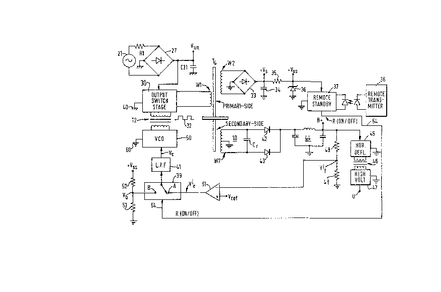
FIGURE 4 illustrates a frequency controlled
resonant regulator 120, embodying the invention, that
provides standby mode and run mode power to a remote
controlled television receiver~ Items in FIGURES 1 and 4
which are similarly identified function in a similar
manner or represent similar quantities.
In FIGURE 4 the AC voltage from mains voltage
source 21 is full wave recitified by a bridge rectifier 27
to develop an unregulated DC voltage Vun filtered by a
capacitor C31. The unregulated voltage is applied to
output switching stage 30 of resonant regulator 120 to
produce an unregulated, 50% duty cycle, sguare wave
voltage across primary winding Wl of resonant power
transformer T4. A regulated secondary side alternating
output voltage is developed across winding W7 in
accordance with the operating point established for tuned
circuit 10 that includes resonating Cr and the inductance
of high leakage transformer T4.
;37~0
-18~ RCA 81,676
The regulated voltage across winding W7 is full
wave rectified by diodes 42 and 43 and filtered by an LC
filter network 44 to develop a regulated DC voltage at a
B+ terminal. The B+ voltage is applied to a horizontal
deflection circuit 45 to generate scanning current in the
horizontal deflection winding of the television receiver,
not illustrated in FIGURE 4. The B+ terminal also
supplies power to a high voltage circuit 47, via
horizontal deflection circuit 45 and a flyback transformer
46. High voltage circuit 47 provides ultor voltage at a
terminal U for the picture tube of the television
receiver, not illustrated in FIGURE 4. Additional
secondary side supply windings, not ~llustrated in FIGURE
4, provide low voltage supplies to other television
receiver circuits such as the vertical, audio, and small
signal circuits.
To regulate the secondary side supply voltages,
a feedback voltage V'f is developed from the B+ voltage by
voltage dividing resistors 48 and 49. Fee~back voltage
V'f is applied to the inverting input terminal of a
comparator 51 to generate a error voltage Vle that is
applied to a contact terminal A of a mode switch 39.
In the run-mode, or full power mode, of
television receiver operation, the on-state of an on/off
command signal R is developed on a signal line 54 coupled
to mode switch 39. During the on-state of command signal
R, the arm of mode switch 39 makes contact with terminal A
to enable the error voltage Vle to be passed on to lowpass
filter 41. Lowpass filter 41 generates a control voltage
Vc for VCO 50 that varies in accordance with the error
voltage V'e.
VCO 50 generates a switching signal 32 at a
frequency that is controlled by feedbac~ voltage V'f.
Switching signal 32 is transformer coupled via an
isolation signal transformer T2 to synchronize the
switching of output switching stage 30 at the frequency of
switching signal 32. Regulation of the secondary side
output voltages is achieved by varying the frequency of
~%~;3~ O
-19- RCA 31,676
switching signal 32 in accordance with the feedback
voltage V'f.
The signal state of command signal R is
controlled by the output of a conventional remote standby
circuit 37. When a user wishes to turn on the television
receiver and provide full power to the receiver circuits,
the user operates a conventional remote transmitter 38
that sends, for example, an infrared signal that is
decoded by standby circuit 37 to switch the state of
command signal R to the on-state. When the user wishes to
turn off the television receiver and place the receiver in
the standby mode of operation, a differently coded
infrared signal is received by standby circuit 37 and
switches the state of command signal R to the off-state.
In accordance with an inventive feature, when
the off-state of command signal R is developed on signal
line 54, the arm of mode switch 39 is moved to make
contact with terminal B, decoupling error voltage Vle from
lowpass filter 41. A bias voltage Vb is developed at mode
switch terminal B by voltage dividing resistors 52 and 53
coupled between the +Vss auxiliary supply terminal and
chassis ground. The value of bias voltage Vb is selected
to produce, when coupled by mode switch 39 to lowpass
filter 41, a control voltage Vc that operates VCO 50 at
its upper limit high frequency operation of f=fmax f
FIGURE 3.
With resonant regulator 120 being operated
during standby at the frequency fmax the operating point
of tuned circuit 10 is well above resonance, resulting in
the loss of secondary side output voltages, such as the B+
voltage. All the television receiver load circuits
powered by the secondary side voltages become inoperative,
placing the television receiver in a standby, low power
state.
In accordance with another feature of the
invention, resonant power transformer T4 provides the
required supply voltage to standby circuit 37 in the
standby or off-state of the television receiver. Even
~3~n~
-20- RCA 81,676
though the transformer is being operated at a very high
frequency during standby, alternating voltages are being
developed by auxiliary winding W2 that is tightly coupled
to primary winding W1.
The auxiliary output voltage across winding W2
is full wave rectified by a bridge rectifier 33 and
filtered by a capacitor 34 to provide an auxiliary DC
voltage +Vs that is unregulated with changes in the mains
derived voltage Vun. Auxiliary voltage Vs is coupled to a
zener diode 36 via a resistor 35 to produce the regulated
auxiliary DC voltage +VSs that is developed not only
during on-state operation of the television receiver but
also during standby operation. Auxiliary supply voltage
+Vss is therefore suitable for use by remote standby
circuit 37 as a voltage supply that is available during
standby mode of operation as well as during run-mode of
operation, or in other words, that is available during
both states of remote on/oEf command signal R.
In accordance with another inventive aspect,
high leakage power transformer T4 may be constructed as a
cup core or pot core transformer. Because of the closed
core configuration of a pot core, radio frequency
interference radiation from the high leakage transformer
is kept relatively low. This results in a further
reduction in radiation beyond the reduction provided due
to the sinewave rather than square wave nature of the
output voltages developed by the secondary side windings.
FIGURE 5 illustrates an exploded perspective
view of the pot core of power transformer T4. ~he
trznsformer core comprises two ferrite pot core e'ements,
a pot core element PCP having a center post leg 62p around
which the primary side windings Wl-W3 of FIGURE l, for
example, are wound, and a pot core element PCS having a
center post leg 62s, not illustrated in the perspective
view of FIGURE 5, around which the secondary side windings
W4-W7 are wound.
In addition to the center post leg 62p or 62s,
each of the pot core elements includes a cylindrical wall
. .
~63~
-21- RCA 81,676
or skirt 61 surrounding the center post leg and a solid
end wall 64. Each of the pot core elements is provided
with gap 63 in cylindrical wall ~1 to enable the lead
wires of the various primary and secondary side windings
to be brought out of the pot core for their connection to
the appropriate circuit elements in regulator 20 of FIGURE
1.
FIGURE 6 illustrates pot core transformer T4 in
the assembled state including the primary side windings,
generally designated as windings P, and the secondary side
windings, generally designated as windings S. Also
illustrated in FIGURE 6 are representative lead wires 65
that are brought out of the tra~ormer core through gap
63. Not illustrated in FIGURE 6 is the conventional
fastening hardware necessary to secure the transformer in
its assembled configuration and necessary to secure the
transformer to a circuit board or chassis.
FIGUR~ 7, illustrates in cross-sectional view,
the assembled transformer T4 through the cross-sectional
line 7-7 of FIGURE 6. In the cross-sectional view of
FIGURE 7, one notes that a gap G is provided between
primary core center post leg 6~p and secondary core center
post leg 62s. An alternative way of providing a gap G,
not illustrated in the figures, is to use two identical
pot core elements PCP and PCS assembled together but
separated from each other by an insulating and
non-magnetizable spacer having a thickness equal to the
desired gap length.
Gap G produces the required loose coupling
between the primary side windings P and the secondary side
windings S, that provides the tuning leakage inductance of
resonant circuit 10 of FIGURES 1 and 4. The loose
coupling permits the secondary side winding voltages to be
of sinusodial waveform and the primary side winding
voltages to be of square wave waveform.
The following is an illustration of a
construction for a inventive embodiment of resonant power
transformer T4 of FIGURE 1.
12~37f~0
-22- RCA 81,676
Core: Two each, ferrite pot core, manufactured
by Ferroxcube Corp., Saugerties, New York, Series 4229,
Part Number 4229P-L00-3C8, modified by extending
cylindrical wall 61 of each by 0.2 inch (5 mm) and by
extending the center post leg 62s by 0.2 inch (5 mm~,
resulting in a gap G of 0.2 inch (5 mm) being developed
when the transformer core is assembled.
Primary Winding Wl: 45 turns of litz wire oE
400 circular mills (0.203 mm2) total cross section, with
the litz wire formed by 25 strands of 0.004 inch (0.10 mm)
diameter enameled copper wire.
Auxili~ry Winding W2: nine turns of litz wire
of 245 circular mills (0.124 mm2) total cross-section,
with the litz wire formed by 20 strands of 0.0035 inch
(0.089 mm) diamete~ enameled copper wire.
Feedback Winding W3: ten turns of litz wire of
245 circular mills (0.124 mm2) total cross-section, with
the litz wire formed by 20 strands of 0.0035 inch (0.089
mm) diameter copper wire.
Secondary Winding W7: 36 turns, center tapped,
of litz wire of 1500 circular mills (0.760 mm2) total
cross section, with the litz wire formed by 60 strands of
0.005 inch (0.127 mm) diameter enameled copper wire.
Secondary Winding W6: two turns of litz wire of
625 circular mills (0.317 mm2) total cross-section, with
the litz wire formed by 25 strands of 0.005 inch (0.127
mm) diameter enameled copper wire.
Secondary Winding W5: three turns of litz wire
of 625 circular mills (0.317 mm2) total cross-section,
with the litz wire formed by 25 strands of 0.005 inch
(0.127 mm~ diameter enameled copper wire.
Secondary Winding W4: eight turns of litz wire
of 625 circular mills (0.317 mm2~ total cross-section,
with the litz wire formed by 25 strands of 0.005 inch
(0.127 mm~ diameter enameled copper wire.
Given the above transformer specifications, the
following is obtained:
~2~7~3
-23- RCA 81,676
L (primary) = 276 microhenry.
L (secondary) -- 196 microhenry.
M (mutual coupling) = 114 microhenry.
k (coeffici~nt of coupling) = 0.49.
Additional values for an arrangement illustrated
in FIGURE 1 are as follows:
Cr = 0 03 microfarad, polypropylene.
fO = 64 kilohertz, nominal op~rating frequency.
Vin = ~150 volts DC.
Input Power = 140 watts.
Q=5, for tuned circuit 10 at 140 watts load
power, to provide extremely high efficiency of around 90%.