Note : Les descriptions sont présentées dans la langue officielle dans laquelle elles ont été soumises.
~Zfi377~
CARRIER WI~VE RECOVERY SYSTEM
BACXGROUND OF THE INVENTION
The present invention relates to a carrier wave recovery
system and, more particularly, to a carrier wave recovery
system for a slotted ALOHA system.
In a slotted ALOHA system which belongs to a family of time
division multiple access (T~MA) communication systems, time
slots each having a predetermined duration are set up
beforehand so that multiple stations may individually transmit
signals in bursts using such time slots. A burst demodulator
adapted to receive the bursts is required to recover on a burst-
by-burst basis a reference carrier wave whose frequency is
synchronous to a carrier wave component. In such a prior art
system, it has been customarY to recover a reference carrier
wave by means of a phase locked loop which consists of
a phase comparator, a low-pass filter, and a voltage controlled
oscillator (YCO) which is phase-locked to a carrier component of
a burst. In a time slot where a burst is not inputted, the VCO is
brought into a self-dri~en oscillation state since the output of the
phase comparator disappears; generally, in this state of the
VCO, the frequency stability is not high. This giYes rise ~o a
problem that in the self-driven oscillation state the VCO
oscillation frequency fluctuates over a substantial range,
resulting in a substanffal difference between a carrier component
frequency and a VCO oscillation frequency, i. e., initial
2 5 frequency offset when a burst with the carrier component
frequency is inputted. Because an initial frequency offset
determines a tuning time of a phase locked loop, a great initial
frequency offset makes the tuning time disproportionately long
,
~26377~
and renders the operation of the phase locked looP itself
unstable.
SUMMARY OF THE INVENTION
It is therefore an obiect of the present invention to provide a
carrier wave recovery system which effects recovery rapidly and
stably.
It is another object of the present invention to provide a
generally improved carrier wave recovery system.
In accordance with the present invention, there is provided a
carrier wave recovery system for recoverin~ a reference carrier
wave from each of burst carrier waves which are sequentially
inputted in bursts at a period which is equal to a predetermined
period of time or an integral multiple of the predetermined
period of time and not a1ways constant, the burst carrier waves
each being not longer than the predetermined period of time.
The system comprises a phase comparator for comparing in
phase each of the burst carrier waves and the reference carrier
wave to produce an error signal, an averaging circuit for
averaging values of the error signals which are associated with
the burst carrier waves inPutted in the past and storing a
resultant mean value, an adder for adding the error signal and
the mean value stored in the averaging circuit, and an oscillator
for controlling an oscillation frequencY in response to an output
~5 of the adder to produce tbe reference carrier wave.
In accordance with the present invention, there is also
provided a carrier wave recovery system $or recovering bY
means of a phase locked loop a reference carrier wave out of
each of burst carrier waves which are sequentially inputted in
bursts at a period which is equal to a predetermined period of
time or an integral multiple of the predetermined period of time
and not always constant, the burst carrier waves each being not
longer than the predetermined period of time. The system
comprises an oscillator an oscillation frequency of which is
3 5 controlled by a control signal, a phase comparator $or
i2fi377~
comparing in phase an output of the oscillator and the burst
carrier wave to Produce an error signal, an averaging circuit fvr
determining a mean value of the control signals, which are
associated with the burst signals inputted in the past, from a
maximum and a minimum values of the control signals and
storing the mean value, and an adder for adding the error signal
and the mean value stored in the averaging circuit and producing
a resultant sum as the control signal. The oscillator, adder and
phase comparator constitutes the phase locl~ed loop so tha~ when
an output of the oscillator has been synchronized to a phase of
the burst carrier wave, that output becomes the reference
carrier wave.
The above and other obiects, features and advantages of the
present invention will become more apparent from the following
detailed description taken with the accompanying drawings.
BRIEF DESCRIPTION OF THE DRAWINGS
Fig. 1 is a block diagram of a carrier wave recovery system
embodying the present invention;
Eig. 2 is a block diagram showing another embodiment of
the present invention; and
Fig. 3 is a timing chart representative of a relationship
between a burst detection signal and a received signal in
accordance with the embodiment of Fig. 2.
DESCRIPTION OF THE PREFERRED EMBODIMENTS
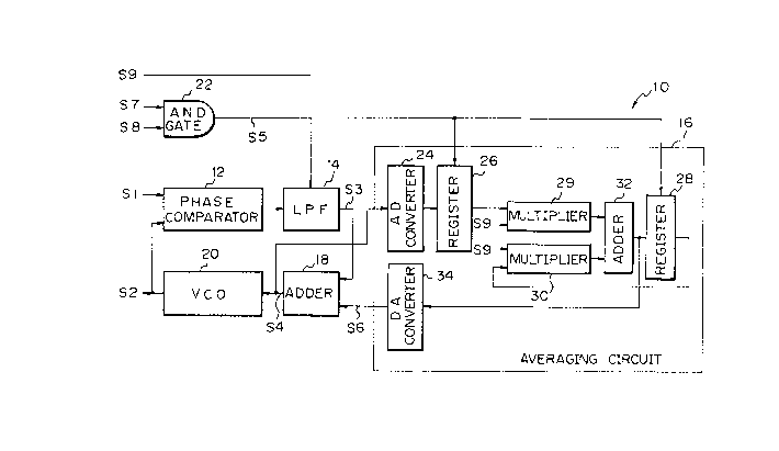
Referring to Fig. 1 of the drawings, a carrier wave recovery
system in accordance with the present inYention is shown and
generally designated bY the -reference numeral 10. As
shown, the system 10 includes a phase comparator 12 adapted
to compare in phase a burst carrier wave signal S1 with a
reference carrier wave signal S2. A result of comparison from
the Phase comparator 12 is applied to a low-pass filter ~LPF) 14
which then produces a low-frequencY component of the output of
35 the phase comparator 12 as an error signal S3. An averaging
l ~fi377~
circuit 16 receives a VCO control signal S4 and a reset signal S5
and, i~ turn, produces an mean signal S6. The error si~nal S3
and mean signal S6 are fed to an adder 18. The output of the
adder 18 is routed to a VCO 20 which is adapted to oscillate the
5 reference carrier wave signal S2. An AND gate 22 functions to
gate a slot timing signal S7 in response to a burst detection
signal S8 and delivers it as the reset signal S5.
The averaging circuit 16 includes an analog-to-digital (AD~
converter 24 for converting the VCO control signal S4 into a
10 digital signal, a register 2 6 for storing an output of the AD
converter 24 which has appeared at the time of entry of the reset
signal S5, and multipliers 29 and 30 for respectively multiplying
data stored in the register 26 and data stored in another register
2 8 by a coefficient signal S9 representative of a coefficient of
0. 5. The circuit 16 further includes an adder 32 for adding
products outputted by the multipliers 29 and 30, the register 28
for storing an output of the adder 32 which has apPeared at the
instant of entry of the reset signal S5, and a digital-to-analog
(DA) converter 34 for converting an output of the adder 32 into
20 the mean signal S6, which is an analog signal.
The carrier recovery system 10 having the above
construction will be operated as follows.
The burst carrier wave signal S1 is a burst-like carrier wave
component which has been extracted from an inputted burst by a
25 Costas loop metho or any other carrier wave extracting method
as well known in the art. In a time slot where a burst is
inputted, the signal S1 is compared with the reference carrier
wave signal S2 outputted bY the VCO 20 by the phase comparator
12, the result of comparison being delivered as the error signal
3 0 S3 via the LPF 14 . The burst detection signal S8 is a signal
which appears when an inputted burst has been surely received
and a unique word has been detected out of the burst. The slot
timing signal S7 is a signal having a constant period
representative of a slot timing. The signal S7 is gated by the
35 AND gate 22 in response to the signal S8. IIence, the AND gate
12fi377:~
2 2 produces the reset signal S5 every time a burst is surely
received.
The operation of the avera~ing circuit 16 will be described
first. At the instant of entry of a new burst, a VCO control
5 signal S4 associated with the latest burst which has been entered
before is held in the register 26 via the AD converter 24. Let the
value of the VCO control signal S4 held in ths register 26 be Vn l,
and the value held in the re~ister ~8 at that time Vn ~. When the
newly entered burst has been surely received, the AND gate 22
10 produces a reset signal S5 with the result that the content of the
register 2 6 is updated to become a ~ontrol signal S4 of this
instant, i. e. a value Vn outputted by the AD converter 24.
Sim~lltaneously, the content of the register 28 is updated to
become Vn. Due to the operations of the multiplier 29 and adder
15 32, Vn is an arithmetical mean of Vn l and Vn l. Hence, until
the next burst is surely received, the output of the adder 32 is
representative of a mean value of digital versions of control
signals S4 outputted by the AD converter 24 and associated one
with each burst received in the past, a later burst being weighted
20 more than an older burst before being avera~ed. The output of
the adder 32 is processed by the DA converter 34 to become an
analog mean signal S6. In the same sense as iust stated, the
mean signal S6 is representative of a mean value of error signals
S3 which lies between the maximum and minimum values of
25 control signals S4, which are associated one-to-one with the
bursts.
The oscillation frequency of the VCO 20 is controlled by a
sum of the error signal S3 and the mean signal S6. In a time
slot with a burst, the VCO 20 is controlled by the sum to be
30 phase-locked to the burst carrier wave signal Sl with the result
that the frequency of the reference carrier wave signal S2
coincides with that of the carrier wave signal S1. In a time slot
without a burst, the signal Sl and, therefore, the signal S3 does
not appear so that the VCO 20, which is suPplied with the mean
35 signal S6 only, oscillates at a frequency corresponding to the
i377~
mean signal S6, i. e. average frequency of carrier wave
components of bursts which were entered in the past.
Assume a case wherein use is made of a low-pass filter or a
phase comparator which makes the error signal S3 indefinite
5 when the burst carrier wave signal Sl is absent. In such a case,
the low-pass filter is discharged by a burst arrival prediction
signal S9 to cause the VCO control signal S4 to coincide with the
mean signal S6. The initial frequency offset at the time of entry
is representative of a difference between a mean frequency of
10 carrier wave components of bursts received in the past and a
frequency of a carrier frequency of a newly entered burst and,
hence, it is smaller than the greatest one of carrier wave
frequency errors associated with the bursts. Because in a time
slot without a burst the carrier wave frequency error of each
15 burst is far smaller than the fluctution of oscillation frequency
under the self-driven VCO osillation condition, the initial
frequency in this particular embodiment is negligibly small.
While the averaging circuit 16 has been shown and described
as performing signal processing in a digital fashion, it may be
20 constructed to effect analog signal processing in which case the
AD converter 24 and DA converter 34 are needless.
As described above, the carrier wave recoverY circuit in
accordance with this particular embodiment is operable rapidly
and stably since in a time slot without a burst it maintains the
2 5 initial frequencY offset very small by controlling the oscillation
frequency of oscillator means to a mean value of carrier wa~Je
signals of bursts receivet in the past.
I
~.2fi377~
Referring to Fig. 2, another embodiment of the present
invention is shown in a block diagram. The carrier wave
recovery system, generally 40, includes a phase comparator 42
for comparing in phase a burst carrier wave si~nal S10 and a
5 VCO output signal S11, an LPF 44 for producing a low-frequency
component of an output of the phase comparator 42 as aD error
signal S12, an Ar) converter 46 for converting an analog VCO
control signal S13 into a digital si8nal S14, a maximum detector
48 and a minimum detector 50 adapted to respectively detect a
10 maximum and a minimum values of incoming bursts out of the
digital signal S14, an averaging circuit 52 for producing a mean
value from outputs S15 and S16 of the detectors 48 and 50, a DA
converter 54 for converting an output signal Sl 7 of the
averaging circuit 52 into an analog means signal S18, an adder
56 for adding the error signal S12 and the mean signal S18, and
a VCO 5 8 .
In operation, the phase comparator 42 compares the phase
of a burst carrier wave signal Sl0 with a VCO output signal S11.
If a burst is inputted, the result of comParison is passed through
20 the LPF 44 to become an error signal Sl2 which is routed
through the adder 56 to control the VCO 58 to therebY complete
a phase locked loop. A burst detection signal S19 is a signal
which appears when, for example, a unique word usually
received together with a burst is detected. A relationship
2 5 between the signal S19 and the received signal is shown in a
timing chart in Fig. 3. Updating operations which the detectors
48 and 50 perform as will be described occur at each positiv~
going edge of the burst detection signal S19.
The VCO control signal S13 is converted into a di~ital signal
30 by the A/D converter 46 and, then, applied to the maximum
detector 48 and minimum detector 50. When the input signal
S14 is greater than the outPut signal S17, the maximum detector
48 replaces the output signal with the input signal. This
manipulation is performed only when a burst is detected. The
35 minimum detector 50, on the other hand, replaces the the input
~.2ti;377~
signal S14 with the output signal S16 when the former is smaller
than the latter. This manipulation, too, is performed only when
a burst is detected.
Because the digital signal S14 is equivalent to the VCO control
5 signal Sl 3, the output frequency of the VCO 58 may be
determined based on the modulation sensitivity (hertz per volt)
of the VCO 58. The signal S15 is representative of a VCO control
signal S13 associated with the frequency of one of input bursts
which has the highest frequency, and the signal Sl 6 a VCO
10 control signal S13 associated with the frequency of one of input
bursts which has the lowest frequency. It follows that the signal
S17, i. e., the mean value of the signals S17 and S16 as
produced by the averaging circuit 5 2 corresponds to the VCO
control signal S13 which correspond to an average frequencY of
15 the lowest and highest frequencies of a received burst signal.
The average frequency signal Sl 7 is converted into an analog
signal by the DA converter 54 to serve as a mean control signal
S1~.
The control signal S20 plays an essential role in resetting the
20 maximum detector 48 and minimum detector 50 at an initial
condition and coPing with long-term frequencY fluctuation which
may occur in the transmission channel. For example, when the
input burst signal frequency has shifted to a higher value due to
the fluctuation of an oscillation frequencY of a satellite rePeater,
25 the minimum detector fails to be updated and, in this condition,
the detectors 4 8 and 5 0 have to be initialized by the control
signal S20 at a lon~ period. The control signal S~1 is adapted to
discharge the LPF 44 iust before a position where a
predetermined burst is to be received, so that the frequency of
3 0 the VCO output signal S11 maY constantly represent a mean
Yalue of the maximum and minimum frequencies of bursts.
It is to be noted that the circuitry consisting of the AD
converter 46, maximum detector 48, minimum detector 50,
averaging circuit 52 and DA converter 54 as shown in Fig. 2
35 may be modified to process signals in an analog fashion in which
3 2~3771
g
case the AD converter 46 and DA converter 54 are needless.
As described above, the carrier wave recovery system in
accordance with this particular embodiment performs recovery
rapidly and stably since a VCO frequency is controlled to an
5 average frequency of a highest and a lowest frequencies of an
input burst signal at the time of initial pull-in.
Various modifications will become possible for those skilled
in the art after receiving the teachings of the present disclosure
without departing from the scope thereof.