Note : Les descriptions sont présentées dans la langue officielle dans laquelle elles ont été soumises.
lZ~ g
TIT1E
FRONT-END S~STEM
FIELD OF THE INVENTION
This invention relates to a front-end sy~tem for
tha conversion of graphical data and coded font data into
a serial pixel bit stream for a raster output scanner
(ROS~ in order to obtain a print~d page.
BACKGROUND OF THE INVENTION
~ ront-end systems for printers which are able to
print a complete page line-wise with serially presented
data are well known. Typically, these conversion systems
are required for laser printers in which a light beam is
modulated image-wise, and in which the modulated light
beam i8 deflected line-wise by means of a polygonal mirror
over a light-sensitive surface. In a known manner a
latent image can be written to the light sensitive surface
by means of the modulated light beam. The latent image is
thereafter developed in a known manner and transferred to
a receiving material such as a sheet of paper.
The graphical data, for example, may be obtained
by scanning an image by means of a scanning device and
storing the data in memory, with or without the aid of a
coding system. The data for a page to be printed is first
processed, for axample by mean~ of a graphical work
station, to produce a finally de~ired layout which may
contain textual and graphical data. If such an assembled
page has to be printed, the graphical data information,
coded or not coded, and the coded font data are fed to the
~ .
~..
~Z~
front-end system along with information relating to
haigh~, width and finally desired position. In addition,
the bit-map information of the characters to be printed is
fed to the front end.
After all the data have been stored in a memory
in the front end, it is necessary to set the data at the
correct location in a page size memory (bit-map memory)
and then to read out the page memory serially and feed the
data to the modulator of a laser printer.
Because modern laser printers are capable of
printing pages at high speed and with a high resolution, a
front-end system will have to be capable of processing the
data for said pages at high speed and presenting them to
the printer.
U.S. Patent No. 4,300,206 describes a raster
printer in which data of any size and orientation can be
printed on a page. A microprocessor receives a succession
of coded character and control data. The coded character
data are processed by the microprocessor one-at-a time in
accordance with the control data and translated into
character bit-map data and after that the microprocessor
positions these data of character bit map into a strip
buffer. However, because the described system operates in
a sequential manner, it is a relatively slow system.
Accordingly, it is an object of the invention to
provide a front-end system which can process the character
and graphical data at high speeds.
, ,.
3LZ69~
--3--
SUMMARY OF THE INVENTION
The present invention provides a high speed
front-end processing system in which the raster image
processor and the raster image memory are connected to
each other by a second bus system.
Generally, the present invention comprises a
front end controller for controlling the front-end which
is connected to the printer and an input/output device.
The controller is also connected to a standard VME bus
(see, e.~., "Backup Support Gives VME bus Powerful
Multiprocessing Architecture," Electronic Components and
Applications, Vol. 6, No. 3, 1984). An input/output
procesæor and memory units are also connected to the VME
bus for storing coded font data and graphical data.
A raster image processor for converting stored
bit representation into a serial pixel-bit for inputting
to a raster output scanner is connected to the VME bus and
to a raster image bus, and includes an output to a raster
scanner. A raster image memory is connected to the raster
image bus for storing the bit representation of a page.
Preferably, the raster image bus is a
synchronous bus having a plurality of multiplexed address/
data lines. By virtue of the second bus, the raster image
bus, the front-end processor controls the front-end system
and collects - data relating to an assembled page
independently of and simultaneously with the raster image
processor which takes care of expanding coded graphical
and font data and placing the data in the raster image
memory. The processor also reads the data out of said
memory, resulting in providing the printer with data in
real time.
12~
--4--
These and other advantages will become apparent
from a perusal of the following detailed description of
presently preferred embodiments taken in connection with
the accompanying drawings.
BRIEF DESCRIPTION OF THE DRAWINGS
Figure 1 is a diagrammatic representation of the
front-end system according to the invention;
Figure 2 schematically represents the processes
performed by the raster image processor;
Figure 3 is a diagrammatic representation of a
raster image processor;
Figure 4 is a diagrammatic representation of a
VME-bus interface;
Figure 5 is a diagrammatic representation of a
laser scan module interface;
Figure 6 is a diagrammatic representation of a
central processing unit of the raster image processor;
Figure 7 is a diagrammatic representation of a
raster image bus interface;
Figure 8 is a diagrammatic representation of a
VME-master interface of the VME-bus interface;
Figure 9 represents the placing of a character
in the bit-map memory;
, ~
_5_ ~64~
Figure 10 represents the results of a number of
possible operations in the bit-map memory; and
Figure ll is a diagrammatic representation of a
raster image memory.
PRESENTLY PREFERRED EMBODIMENTS
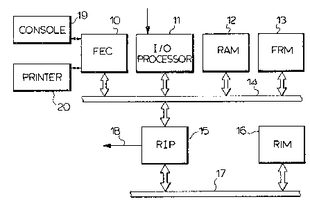
Figure 1 is a diagrammatic representation of a
front-end system. As shown a front-end controller 10
(FEC) is connected to an operating console 19 and also to
the control system of a printer 20. Printer 20 is a
raster output scanner in which a light beam is modulated
image-wise and i9 deflected line-wise over the surface of
a light-sensitive element. The light-sensitive element is
driven perpendicular to the direction of deflection of the
light beam in order or it to be possible to write a
complete image in raster form. ~n example of a raster
output scanner is a laser printer in which a modulated
laser beam is driven by means of a rotating multiface
mirror over the surface of a charged photoconductor. The
photoconductor is exposed image-wise in this process, and
the charged image obtained can be developed in a known
manner with toner, then transferred to a receiving sheet
and fixed by means of heat.
Front-end controller 10 preferably contains a
16-bit microprocessor system embodying, for example, a
Motorola 68000 microprocessor and functions in combination
with local ROM and a part of a random access memory 12
(RAM) as the control system for the front end. In font
read memory 13 are stored the bit patterns of a number of
print types. The front end ~ay be connected via an I/0
processor 11, which also contai~s a 16-bit microprocessor
system embodying a Motorola 68000 microprocessor, to a
~' Trade Mark
,
-6-~2~
disc memory, work station, computer and/or cluster
controller. The FEC 10, I/0 processor 11, RAM 12 and font
memory 13 are connected to each other via a standard VME
bus 14. The font memory 13 can also be constructed as a
RAM or form part of RAM 12. The bit patterns of the fonts
are then loaded into said RAM from a disc memory or
floppy-disc memory.
- A raster image processor 15 (RIP) is also
connected to VME bus 14. In addition, raster image
processor 15 is connected via a raster image bus 17 (RI
bus) to a page-size bit-map memory 16, also termed raster
image memory (RIM). RIP 15 serves to fill the bit-map
memory 16 ~RIM) image-wise with type characters that are
called up from font memory 13 and deposited in the correct
location in bit-map memory 16. In addition, RIP 15 can
call up graphical information from memory 12 and also set
it aside at the desired locations in bit-map memory 16.
If the bit-map memory has been filled, it can be read out
again via RIP 15, the data read out being fed as a serial
pixel-bit stream via line 18 to the modulator of the laser
printer.
The image which is written on the photoconductor
is made up of pixels preferably having a size of 0.05 x
0.05 mm so that approximately 4,000 x 6,000 pixels are
necessary to print an A4-format black/white image.
Conse~uently, bit-map memory 16 is preferably
approximately 24 megabits or 3 megabytes. During raad out
of bit-map memory 16, the pixel bit rate to the modulator
of the laser printer via line 18 is approximately 25
megapixels/sec, resulting in the printing of an A4-format
page in approximately 1 sec.
~2~;4~L"3~
All data relating to a page to be printed are
stored in RAM 12 via I/O processor 11 from, for example, a
work station and under the control of FEC 10. For this
purpose various options are available, for example, an A4-
page, which has to be printed in the "portrait mode."
Approximately 4,000 subtables are made corresponding to
the approximately 4,000 scan lines which are necessary to
write a page. In each subtable, type codes of the type
characters or graphical characters are stored which have
their starting point on a certain scan line. Each type
code contains, in addition, data relating to the X
position which the character assumes on the scan line,
data relating to the font type and also data relating to
the height and width of a certain character. The type
code also contains data relating to a base address in the
font memory 13, where the bit representation of said
character is stored in 16-bit words. The set of lists
thus formed is termed the list of primitives.
Once the data relating to a page to be printed
have thus been stored in RAM 12, filling bit-map memory 16
can be started. For this purpose the letter codes are
called up from RAM 12 one by one by RIP 15 and, together
with the associated bit representation from the font
memory 13, expanded and deposited at the correct X and Y
locations in bit-map memory 16. In a corresponding manner
all characters are completed one by one until bit-map
memory 16 is completely filled with the pixel
representation of the page to be printed.
It is not necessary to form sublists. The data
relating to a page to be printed can also be stored in the
RAM 12 in a random sequence. During the filling of bit-
map memory 16, RAM 12, in which the primitives are placed
" .
~Z~;4~9
in a random se~uence, is successively read out, expanded,
and placed at the respective locations in bit~map memory
16.
In a preferred embodiment all of the characters
occurring on a page are stored only once and provided with
data relating to the various positions which each
character assumes on the page. In this manner, the data
relating to a frequently occurring character such as, for
example, the letter "e", are only stored once in RAM 12
and all the positions which this letter assumes on the
page are inserted in a separate table.
Usually first the graphical characters which are
stored in RAM 12 or font memory 13 are placed in bit-map
memory 16 and only thereafter the type characters.
The Raster Imaae Processor
Referring to Figure 2, the processes carried out
~y the raster image processor 15 are shown schematically
(RIP). After starting up the system (Step 24), RIP 15 is
initiated (Step 25) (INIT command) by a system reset or an
INIT command from front-end controller 10. A "self test"
process (Step 26) is started which comprises the testing
of various RIP functions and bit-map memory (RIM)
functions. RIP 15 must not have access to VME bus 14
during the self-test procedure, because the FEC 10
requires the VME bus 14 for the testing of RAM 12 and font
memory 13. If RIP 15 successfully carries out the "self-
test" program, an interrupt signal is transmitted to FEC
and RIP 15 goes into the wait mode (Step 27). If the
self-test program has detected a fault, RIP 15 also goes
into the wait mode (Step 27), but no interrupt signal is
~L2&i4~
g
generated for the FEC 10. In this manner front-end
controller 10 knows that a fault has been diagnosed in the
RIP 15 "self test". A fault is also indicated to the
operator by a LED lighting up.
On an I'RIP diagnosis" cor~mand from FEC 10 to RIP
15, RIP 15 diagnosi~ process 30 starts. The RIP 15
performs a number of internal tests and also a number of
tests on RIM 16. The results of these tests are stored in
RAM 12 and can be transmitted to, and made visible on,
operating console l9. The RIP diagnosis process also
test~ the VME interfaces. The RIP diagnosi process has a
more extensive character while the self-test process
performs a more functional hardware test. After the
termination of the RIP diagnosis process, RIP 15 stores
status information in RAM 12, generates an interrupt
signal for FEC lO, and unblocks VME bus 14.
After RIP 1~ has received a '1fill bit map"
command from EEC 10, RIP 15 checks the data transfer on
VME bus 14. RIP 15 thus acquires access to RAM 12, which
contains the primitives o the page which has to be
printed.
RIP 15 expands the list of primitives by means
of the pixel representations of the fonts and deposits
these in bit-map memory 16 (RIM). RIP 15 has acce3-q to
RIM 16 via RI bus 17. RIM 16 contains, in addition,
modification logics which supports RIP 15 in performing
various arithmetical op~rations on data for bit-map memory
16 such as, for example, AND, OR and INVERT operations.
After the bit maR has been filled (Step 28), RIP 15 stores
status information in RAM 12, generates an interrupt
signal for FEC 10, and unblocks VME bus 14.
. . .
,,
--10--
FEC 10 then generates a "read bit map" command
and RIP 15 waits for a page synchronization signal whi~h
originates from the laser printer via a control interface.
After the page synchronization is ~enerated, RIP 15 starts
by reading out RIM 16 (Step 29) and generates a serial
pi~el bit stream which is fed to the modulator of the
laser printer via a video interface. After the
termination of the bit-map reading process (step 29), RIP
again stores status data in RAM 12, generates an
int~rrupt signal for FEC 10, and then unblocks VME ~us 14.
With reference to Figure 3, Rip 15 preferably
includes an internal bus system having raster image
processor bus 46 (RIP bus~ which is a syn~hronous bu~
designed to exclusively transfer 16-bit words. RIP bus 46
contains data lines 47, address and control lines 48 and
condition lines 4~. The RIP bus is connected via a VME
bus interface 41 to VME bus 14, and, via an RI bus
interface 45, to RI bus 17. RI bus 17 contains, inter
alia, data and addre~s lines 58, a busy line 57, an RI bus
address available line 56, a clock line 54, and
modification lines. In addition, RIP bus 46 is connected
to a laser scan module interface 44 (LSM interface) and
the central processing unit 43 (CPU) of RIP 15. The laser
scan module LSM interface 44 is connected to lines
originating from the printer. For example, "start-of-
scan" line 52 (SOS), by which a synchronization signal is
supplied to indicate the beginning of a line to be
printed, a burst line 53, by which a signal is supplied
which corresponds to the desired pixel frequency, and a
video line 18, by which the serial pi~el bit stream is fed
to the modulator from the laser printer on reading out
bit-map memory 16. The addre~s and control lines 48 and
the condition lines 49 are also further connected to a
page synchronization interface 42. A "page-available"
, ,.
~1 2~4~
--11--
signal (PAV) is fed to the control device of the printer
via line 50. This signal indicates that a page is fully
formatted in bit-map memory 16 and that RIP 15 can start
r~ading out bit-map memory 1~ on receiving a "start-o~-
pag " signal (SOP) via line 51 which is derived from the
control device of the printer.
VME-Bus Interface
~ eferring to Figure 4, VME-bus interface 41 is
diagrammatically represented in detail. A master
interface 100, a slave interface 101, and an interrupter
102 are connected to VME bus 14. Data lines 47 from RIP
bus 46 are connected to master interface lO0. The address
and control lines 48 are connected, as are the condition
lines 49 ~rom RIP bus 46, to master interface 100, slave
interface 101, and interrupter 102. The task of the VME-
bus interface 41 is to shield RIP 15 from the asynchronous
VME bus 14. The VME master interface 100 (VME-MI)
contains an internal control system ~y means of which the
buffers and registers present are controlled. This
interface permits access cycles to be performed on the VME
bus 14. In the control system, programmable logic is
used. For the control of slave interface 101 and
interrupter 102 preferably programmable logic is provided.
With reference to Figure 8, V~E-~I 100 also
comprises data transfer functions. These functions
include data base-master (DTB-master) and data hase-
requester (DTB-requester). To achieve the desired speed
in the data transfer VME-MI 100 includes additional
functions.
-12-
The first function is an address up/down counter
formed by an address high counter 132 and an address low
counter 133. During the loading of RIM 16 with the bit
representations of the various type characters or
graphical characters which are each stored separately with
~onsecutive addresses in font memory 13 or RAM 12,
counters 132 and 133 are preset for each character with
the base addresa of said character in, for exar~ple, ~AM
12. Via buffer 134 and the VME address bus 141 of VME bus
14 the base address is supplied to R~M 12, and the first
16-bit word at the respective memory location is supplied
via VME data bus 142 of VME bus 14 to a bidirectional
buffer 135 and then placed at the correct location in RIM
16. The subsequent address for RA~ 12 is generated by
increasing counter 133 by 1 and the second 16-bit word is
supplied to RIM 16 by VME-MI lOO. In a corresponding
m~nner all of the addresses associated with a given
character are generated until such time as that character
has been completely written into RIM 16.
In this manner CPU 43 needs to generate a base
address only once per character so that during loading
other ~unctions can be performed, for example pixel
processing operations, RIM address determination, and the
like.
After a character has been finished, a new base
address for a subsequent character is fed to counters 132
and 133 and the cycle described above is repeated.
The second function, the mirror function, is
performed with a mirror circuit 136 which is constructed
with programmable logic such as FPLAs or PALs and which
can be used if characters have to be set rotated through
.
~Z6~
180 in RIM 16. Mirror circuit 136 interchanges bit 0 of
a 16 bit word with bit 15, bit 1 with bit 14, bit 2 with
bit 13, etc.
The CPU 43 does not now generate the base
address, but calculates, from data relating to -the length
and width and base address of a character, the highest
occurring address for said given character in R~ 12.
This highest address is loaded into counters 132 and 133
while the counters are also switched over to down~counters
by VME~MI controller 130. After each memory access of RAM
12 the content of counter 133 is reduced by 1 and the 16-
bit words from RAM 12 are mirrored in mirror circuit 136
and placed in the RIM 16 via data-in register 137. These
cycles are continued until the original base address of
the character is reached. In VME-MI lO0, a data-out
register 138 is also connected via data lines 47 to RIP
bus 46 in order to feed data in this manner to, for
example, FEC 10 or to RAM 12.
VME-MI controller 130 is connected via control
lines 48 and condition lines 49 to RIP bus 46 and, in
addition, via buffer 131 to address, data and control
lines 139 and bus arbitration lines 140 of VME bus 14.
CPU 43 can call up various modes in VME-MI 100,
such as "release bus", "multiple access", "single access"
and "change". Before VME-MI 100 can switch to the single-
or multiple-access mode, the following data must first
also be specified: read or write, normal or mirrored, the
desired address and the data to be processed. These
specifications can only be altered during the "release
bus" mode and during "change" mode. However, the data to
be processed always may be changed. This is indicated by
-14- ~6~
a 'CHANGE ACKNOWLEDGE" line. The register which contains
the read data from VME bus 14 can always be read out if a
"REGISTER FULL" line is active.
After calling up a "release bus" mode, VME-MI
100 will unblock VME bus 14. This means that the VME-bus
drivers are disabled and a BUSY signal from the VME bus is
rendered inactive. The unblocking of VME bus 14 can only
take place if the last access cycle is completely
finished. A "OE ~ GE ACKNOWLEDGE" signal indicates that
the "release bus" mode is established. In this mode of
the interface no access to VME bus 14 can take place.
After a l'change'l request, VME-MI 100 is in~tructed to
seize VME bus 14 if this was not yet the case. This is
achieved with the bus arbitration lines 140. the
assumption of the "Change" mode is indicated via the
"CHANGE ACKNOWLEDGE" line. Access to VME bus 14 can then
take place. The contents of the address and data
registers also can be changed in the llchangell mode. The
"change" mode provides a possibility to stop accesses to
the VME bus temporarily without the VME bus being
unblocked. A single access to the VME bus can be
initiated by calling up a llsingle cyclel' mode. If the
preceding mode was a llrelease busll mode the VME bus is
only seized via a corresponding active signal from the
arbitration logic. Thereafter only a word access to the
VME bus can be performed.
A read/write indicator decides whether a read or
write cycle has to be performed. A read cycle means that
data from VME bus 14 is clocked into data-in register 137
via mirror circuit 136. Circuit 136 can be activated by
means of a normal/mirrored indicator. When data is being
clocked into data-in register 137, a REGISTER-FULL flag is
set to indicate to CPU 43 that the transfer of data is
-15- ~2~4~
complete and that the data have entered the register. The
REGISTER-FULL flag is set at the instant at which the data
is read into data-in register 137, and after this access
the content of the address counter is increased by 1. If
a mirror function has been enabled, the content of the
address counter is decreased by 1. If the REGISTER-FULL
flag is still activated and data is being read from the
VME-bus, the normal VME cycle is prolonged until the data-
in register has been completely read out and new data have
been read into data-in register 137.
A write cycle is in principle the same as a read
cycle. Th~ only difference is the direction of the data
stream. In a write cycle the data which are in data-out
register 138 are transferred to VME bus 14. Mirror
circuit 136 does not alter anything in the written data.
The data-in register 137 must already have been read for
it to be possible to clear the REGISTER-FULL flag.
The "multiple-access" mode exhibits many
similarities to the "single-access" mode. A "single~
access" mode is intended for the reading and writing of
commands from, and status information to, the FEC. A
i'multiple-access" mode is primarily intended for reading
graphical and font data, a subsequent access being
automatically initiated by VME-MI 100. The new address is
generated by the address counter. The only action which
has to be performed in this case is the reading of data-in
register 137.
The various modes described above are selected
with the VME-MODE lines which are connected to some of the
signal lines of CPU 43. The read/write selector and the
normal/mirrored selector are also connected to such signal
lines. The CHANGE-ACKNOWLEDGE and VME register-full
~z~
-16~
signals originate from the WAIT lines of CPU 43. The VME
address is stored in 24-bit counters 132 and 133, the
input and output data in two 16-bit registers 137 and 138.
'7Address-high" and 'Jaddress-low" counters 132 and 133 and
the data-out register 138 are loaded by means of register
clock lines. The data-in register 137 can be read by
means of a register enable line originating from CPU 43.
The LSM Interface
In Figure 5, the LSM interface 44 is
diagrammatically represented. Upon reading out RIM 16,
RIP 15 fetches a 16-bit word from memory and transmits it
via data lines 47 of RIP bus 46 to register 111. Control
block 110 sends a "load" signal via line 115 to shift
register 112 and the content of register 111 is loaded in
parallel into the shift register 112. The laser printer
emits burst pulses with a frequency of approximately 24
MHz which are supplied via line 53 and I/O buffer 113 to
shift register 112 and control block 110. The contents of
the shift register 112 is serially shifted out by means of
said pulses and is supplied via I/O buffer 113 via line 18
to the modulator of the ROS.
The burst pulses are supplied to a 16 counter in
control block 110 so that once 15 pulses have been counted
or during the 16th counting pulse, a word which has now
been freshly set in register 111 is transmitted in
parallel to shift register 112 and shifted out. Before
the shifting-out operation of the 16-bit word is started,
however, register 111 is loaded with a new 16 bit-word.
An "EMPTY" flag is set once data have been set in the
shift register 112 and new data can be written into the
register 111. The l'EMPTY't flag is connected to a "wait
line" of the CPU 43 of the RIP 15. In this manner a whole
-17- ~2~4~9
scan line is transmitted in se~uence to the ROS. The
control block 110 emits condition signals to the CPU 43
via condition lines 49 of the RIP bus 46. After a scan
line has been completed and before a SOS signal is
supplied via line 52 from the ROS to control block 110,
the fetching of data from RIM 16 is briefly suspended by
RIP 15 (wait condition). During this time the register
111 is cleared via line 114. In response to the SOS
signal the cycle of filling register 111, transmission to
shit register 112, shifting out etc., described earlier
is repeated again for a subsequent scan line. After the
loading of a word into register 111 the "full" status is
likewise transmitted via condition lines 49 to CPU 43, the
latter delaying the fetching up of a new word until the
content of register 111 has again been loaded into shift
register 112. After a PAV signal the number of SOS pulses
is counted by means of a counter in CPU 43, and by this
means it is possible to ascertain when a page has been
transmitted completely to the ROS.
The Central Processin~ Unit
Referring to Figure 6, CPU 43 of RIP 15 is built
around a microprogrammable microprocessor, processor 74,
such as a type Am29116, and an associated addrass
sequencer 70, such as a type 2910A, both manufactured by
Advanced Micro Devices.
In response to each clock cycle the
microinstruction which has to be performed is set in the
microinstruction register 72. Said microinstruction
originates from micro-PROM 71 and the latter is again
addressed by means of the address sequencer 70. In
processor 74 every function is controlled by some of the
-18- ~Z~4~
microinstruction bits. The microinstructions can be
divided into bits for address sequencer 70, processor 74,
branch-address control unit 79, condition selector 75,
wait selector 77, and enable block 7~.
The seoiuence in which the microinstructions
stored in the micro-PROM 71 are performed is likewise
controlled by address sequencer 70. In addition to the
possibility of consecutive access to the addresses,
conditional branch instructions to every microinstruction
in the 4096-size microword area of micro-PROM 71 can be
carried out. A LIFO stack provides return-coupling and
loop-in possi~ilities in a microsubroutine. The stack is
nine steps deep. For each microinstruction the address
seguencer 70 provides a 12-bit address which is initiated
from one of the four following s~urces:
The microprogram address register (PC), which usually
indicates an address by an address increase of 1 with
respect to the address being handled. However, if a
"wait" mode is generated by wait selector 77, the PC
is not increased.
An external input connected to lines 92 which obtains
its data from the branch address control unit 79.
A nine-step deep LIFO stack which is loaded with the
content of the microprogram address register (PC)
during a preceding microinstruction.
A register/counter which retains the data which have
been loaded from an external input during a preceding
microinstruction.
--19--
Processor 74 is a microprogrammable 16-bit
microprocessor, preferably a type Am 29116, with an
instruction set which is optimized for graphical
applications. The instruction set for processor 74
comprises, in particular, single and double operand,
rotate n bits and rotate and merge.
Processor 74 receives its instructions for
performing an operation from the microinstruction register
72 via bus a3 and an instruction-modification circuit 7.3.
The instruction input is also used as data-input
for "immediate" instructions. If the "instruction-enable"
(IEN) input of the processor 74 is activated via line 94,
the results of the instruction performed are retained in
the accumulator and the status register in the processor
74. If an "output enable" (OE) is activated via line 95,
the data lines of the CPU 43 are switched as outputs and
they contain the content of the ALU of processor 74.
Conversely, if the "output enable" is rendered inactive
via line 95, the databus of CPU 43 functions as a 16-bit
input, and data which are present on the RIP bus can be
supplied via data lines 47 to processor 74. Data can then
be retained in an internal register. The data bus of
processor 74 is connected directly to the data lines 47 of
the RIP bus.
The status of the ALU (for example, carry,
negative, zero, overflow) is available on the "status ~us"
87 of processor 74 during each cycle. Instruction-
modification circuit 73 makes it possible to adapt the
instructions recorded in micro-PROM 71 to indicate in the
case of instructions such as, for example, "rotate n
., ,
-20-
bits", the number of bits with which rotation has to be
performed. This number of bits is then specified via a
number of lines (91) from processor data lines 47.
If an IEN signal on line 94 renders the
instruction input of processor 74 inactive, the same
processor instruction bits which are supplied to processor
74 on bus 83 can be supplied via bus 84 also to the branch
address control unit 79 and be used to cause address
seguencer 70 to branch to a randomly different address.
Normally unit 79 receives its branch address from the
content of a register which is filled with data from data
lines 47 via bus 90.
The condition selactor 75 incorporates a one-
out-of eight multiplexer, and the output thereof is
connected via line 89 to address sequencer 70. One of the
eight possible conditions which are applied from condition
lines 49 of the RIP bus or from the processor status lines
87 via status buffer 76 and lines 88 to the input of
condition selector 75 can be selected. The selected
condition is used by address sequencer 70 to perform the
desired conditional instruction. Any new conditions can
be loaded into status buffer 76 by supplying a selection-
enable signal (SLE) via lines 85 to status buffer 76.
The "wait selector" 77 also incorporates a one-
out-of-eight multiplexer which, in the active mode,
connects one of the eight "wait" lines 97 via line 93 to
address sequencer 70. A zero level on a wait line stops
the program counter of the program address register. The
wait lines are connected to the condition lines of the RIP
bus.
~2~
-21-
The enable block 78 have various functions and
generates, in addition, all the signals which are
necessary for the control lines on the RIP bus. It
performs three different functions:
- a. The generation of "enable signals".
The enable signals determine which of the data
registers which are conn~cted by their outputs
to the RIP bus have to be activated. For each
register there is one enable line.
b. The generation of register clocks.
The clock lines determine which data registers
which are connected by their inputs to the RIP
bus have to clock in data. There is one clock
line present for each register.
c. The generation of other signals.
The signals on the signal lines are used as
flags and function selectors in the interface
modules which are connected to the RIP bus.
Raster Imaae Bus Interface
The connection between RIP bus 46 and RI bus 17
is formed by the RI bus interface 45 shown in Figure 7.
Interface 45 buffers the bidirectional data, the addresses
to be called up and the modification code. The buffering
is performed by means of various registers, including
"data-out" register 120, "address-low" register 122,
"address-high" register 123, and modification register
124. These registers can be loaded from RIP bus 46. The
-22-
loading takes place under the control of address and
control lines 48 of the enable block 78 of CPU 43. The
'Idata-in'' register 121 can be read out under the guidance
of control by means of an enable line of enable block 78.
The "address~high" register 123 contains the most
significant bits of the address. The "address-low"
register 122 contains the least significant bits. After
the loading of "address-high" register 123 the RI-bus
read/write cycle is automatically started. This means
that the following processes are carried out by controller
125:
Cycle 1 ~ sets an address on the RI bus and
activates RAV (RI-bus address valid),
Cycle 2 - sets data-out on the RI bus and
inactivates RAV, and
Cycle 3 - reads the data on the RI bus into the
"data-in" register 121.
Before the starting of an RI-bus cycle, CPU 43 has to test
whether the RI-bus busy line 57 is inactive. A busy line
57 is connected to one of the wait lines of CPU 43.
The Raster Ima~e Bus ~RI Bus)
RI bus 17 connects RIP 15 to bit-map memory 16
(RIM) and is made up of 64 lines. It comprises a 32-bit
wide multiplexed address/data bus. RIP 15 acts on RI bus
17 as a master. The RIM 16, which comprises one or more
RIM boards, does not itself take any initiative on the
bus. In addition, RI-bus DMA devices which can submit a
request to the RIP 15 to obtain control over the bus can
be connected to RI bus 17.
-23- ~Z6~9
RI bus 17 is a synchronous bus. A clock signal
(BCLX3 is presented to the RI bus by RIP 15. All of the
actions on the bus are performed at the edges of the
biphase clock. Thus, all of the actions of the RIP take
place on the rising edge, and all the actions of the RIM
on the falling edge of the clock signal (BCLK). The other
modes on RI bus 17 can be described by means of three
signal levels, high, low and high-impedance (tristate).
All of the alterations in signal levels take place after
they have been initiated by an active edge of the biphase
clock. There are thus three groups of signals: the clock
signals, the address/data signals, and the remaining
signals.
The signals which occur on the bus are:
(a) BCLK: a symmetrical clock pulse which
is presented to the RI bus by the RIP.
(b) RAD 00.... RAD 31 (RIP address/data lines):
a multiplexed address/data way which is driven
by all of the bus devices with tristate drivers.
All of the lines are active when "high".
(c) RBR O, RBR 1 (RI-bus bus request): with these
open-collector signals two DMA devices can
request the bus arbiter for access to the bus.
The devices are of different priority.
(d) RROFF (RI-bus refresh-off): a signal indicating
that the RIM boards can switch off the refresh
to achieve a minlmum cycle time. To prevent
loss of data, a special addressing sequence is
maintained between the RIM boards and the RIP.
,~.
, . . .
, . . , . .. ~ . . ... .. . . . . . .. . . .. .. .. .
-2~-
lZ~4~ ~
(e) RBG (RI-bus bus grant): with this line the bus
arbiter indicates that the bus is available to
the requesting device with the highest priority.
(f) RBUSY (RI-bus bus busy): with this open-
collector signal an addressed RIM board can
indicate that the board is unable to process a
new bus cycle for a certain time.
(g) ~AV (RI-bus address valid): This tristate
signal which is active when low indicates that
there is a valid address on the RI bus.
(h) RMC O ... RMC 3 (RIM modify code): on these
lines a code is presented to the RIM board by
the RIP or a DMA device. This code specifies
the "modify" function which takes place during
the logic operation which is performed on the
RIM board on the content of the addressed memory
word. These signals are also of the tristate
type.
The RI bus is constructed with a 32-bit wide
data and address way which is multiplexed for RAD 00 ...
RAD 31. The allocation of these lines is as follows:
A 24 - D 16: in this situation, address lines RAOO
... RA23 are used. The lines RAD 24 ... RAD 31 are
then in the "don't care" mode. For data lines RADOO
... RAD 15 are used. Lines RAD16 ... RAD31 are at
that instant in the "don't care" mode. Data transfer
thus takes place on the basis of 16-bit words and the
addresses are 24 bits wide.
. . ,
-25-
Another option for using the 32 data and address
lines is: A24 - D16 - D16: This situation is the same as
the A24 - D16 situation as regards the address lines. By
adding a second board in the same address space, in which
the data flows through the bus via the lines RAD 16 ...
RAD31, it is possible for a 32-bit wide databus to be
created with two boards which are internally 16 bits wide.
On a RIM board it is possible for the section of the
address/databus over which the data is transferred to be
selected.
By means of the RBR0, RBR1 and RBG signals
access to the RI bus is regulated between the RIP and
optional DMA devices. This arbitration takes place
completely outside RIM 16.
Each cycle on the bus consists of a WRITE/READ
cycle. If the bus is free (RBUSY not active), the RIP is
able to set an address (ADR[n]) on the bus on lines (RADOO
... RAD23). This ta~es place together with the
presentation of a RAV-signal and a RI-bus modify code (RM
code) via lines RMC00 ... RMC03. After the address the
RIP presents its data (DATA0[n]~ to the bus on lines
(RAD00 ... RAD15).
The RIM board addressed by ADR[n] renders the
RBUSY signal active. The RIP then leaves the RI bus in
order to give the RIM board addressed by the ADR[n-l] the
opportunity to set DATAI~n-l] on the bus so that the RIP
is able to read these data in. Two consecutive WRITE/READ
cycles are, as it were, pushed into each other as a result
of this. This is still further optimized by making the
time which the RIP reguires to decide whether RBUSY has
become inactive coincide with the last processing phase of
.~64~
-26-
the RIM board addressed by ADR[n] in the current cycle.
This is achieved by the RIM board making RBUSY already
inactive before the RIM board is already completely ready
but when it is already quite certain that it will be ready
when the RIP has been able to confirm this. The first
cycle thus contains invalid data and an additional cycle
is also necessary to fetch up the final data from the RIM.
In the manner described above, a minimum cycle
time is achieved on the bus. "Minimum cycle time" is the
timing sequence of bus modes in which a maximum transfer
rate is achieved on the bus.
As a result of the refresh of the RIM it may
happen that a RIM board is unable to achieve the minimum
cycle time. The RIM boards indicate this by means of the
RBUSY signal. By extending this RBUSY signal by a certain
number of clock cycles (BCLK~, the RIP postpones its
subsequent access to the memory by an integral number of
clock cycles.
A same situation may occur if the RIP has not
yet finished a certain task. The RIP indicates this to
the bus by postponing the R~V signal by an integral number
of clock cycles.
Raster Imaae Memory
RIM 16 shown in Figure 11 comprises a 24 Mbit
dynamic memory 220 organized in 16-bit words which is used
as a page-size bit-map memory. Each memory location in
the memory 220 corresponds to one precise position on the
final printed page. RIM 16 is connected via RI bus 17 to
RIP 15 and is filled by RIP 15 with expanded font data and
graphical data. An important process which takes place in
,.. .
~64~
-27-
RIM 16 is the modification process which is performed on
an addressed word. The modification process comprises 16
different logic operations which can be applied to the
incominy data and the data already present at a certain
address. One particular modify function is selected by
presenting a RIM modify code to the lines RMCO ... RMC3
221 of RI bus 17.
The modify code is set in the RMC register 222
and supplied to logic processing unit 223 (ALU) which i~
made up of programmable logic. The new data (ND) is
supplied via DATAO register 227 over data lines 225 to ALU
223 while the old data (OD) already present in the memory
220 is supplied via data output lines 226 to ALU 223. The
re~ult of the processing (MD) in ALU 223 is written into
the memory 220 via lines 224.
In the table below, some of the modify functions
are repxesented along with the RM codes associated
therewith and the coxresponding logic functions.
....
~6~3Lg~
-28-
Modify function RMC Logic function
3 2 1 0
WRITE 0 0 0 0 ND
PAINT 0 0 0 1 ND.OR.OD
MASK 0 0 1 0 ND.AND.OD
ERASE 0 0 1 1 ND.AND.OD
I NVERT O 1 0 0 ND
INV. PAINT 0 1 0 1 ND.EXOR.OD
NOP 0 1 1 0 OD
CLEAR 0 1 1 1 ZERO
SET 1 X X X ONE
ND = new data
- OD = old data
Because RI bus 17 is a multiplexed bus, the
separate addresses and the data are clocked into the
xegisters. For this purpose RI bus 17 is connected to an
addre~s/data bus buffer 228, and when an address is
presented to the RI bus 17, it is supplied to address
register 229 via buffer 228. When the data is presented
(one clock cycle later), the data are stored in the DATO
register 227 via buffers 228. The data-in register 233
("in" for the RIP but "out" for the RIM) is provided to
set the data originating from the memory 220, which
belongs to the previously presented address, onto RI bus
17.
.-. ~
1Z,6L.~L99
-29-
The control of RIM 16 is provided by memory
control circuit 231. Memory control circuit 231 contains
a bus state sequencer for starting a number of actions in
response to a RAV signal. These actions consist of the
clocking in of an address, the clocking in of data
associated therewith, the clocking in of the modify code,
and the setting of data belonging to the preceding address
on RI bus 17. In addition, memory control circuit 231
incorporates a memory state sequencer which is
synchronized with the bus state sequencer. The memory
state sequencer can be initiated by a refresh request or
by a bus cycle for a memory access. If a refresh cycle is
performed, the next bus cycle has to be suspended. The
circuit 231 employs programmable logic.
Memory 220 is made up preferably of 256 K
dynamic memory chips and is organized in six "banks" of
256 K words of 16 bits. Bank selection takes place
through decoding the address lines A18, Al9 and A20 in
address multiplexer 232. The addressing of a memory
location in one bank takes place by means of address lines
A0 - A7 and A16 and the generation of a row address strobe
(RAS) from control circuit 231, and address lines A8, Al5
and A17 are then supplied to the memory address lines via
address multiplexer 232, and a column address strobe (CAS)
is also generated by control circuit 231.
Because dynamic memories are used, preferably,
all the memory locations of memory 220 undergo a refresh
at least once every 4 msec. This is done by periodically
adding a "RAS-only" cycle. During this cycle a row
address is presented to all the banks. The refresh
address in a row is derived by means of a 9-bit counter
which is increased by 1 after each refresh cycle.
~ 4199
-30-
By activating the RROFF line of RI bus 17 the
normal refresh cycle is interrupted and RIP 15 ensures
that the minimum cycle time of the next cycle is met.
Non-addressed banks of the memory then use the address on
RI bus 17 to perform a refresh. On the addressed bank
refresh takes place by an access to the selected address.
If only one copy of a page has to be made, the
"CLEAR" modify code will be set on RI bus 17 during the
reading out of RIM 16 because after reading out RIM 16
must be completely filled with zeros. If the page has to
be kept in order to be printed yet once more, the "NOP"
modify code will be set on RI bus 17.
Graphical Instructions
The bit-map filler 2~ as shown in Figure 2 is
designed to perform various textual graphical instructions
such as CHAR, MCHAR, VLINE, HLINE, BLOCK FILL, AREAFILL,
LINE and CIRCLE.
All these instructions, which are stored in
micro-PROM 71 as shown in Figure 6, are performed as
microinstructions for CPU 43. The algorithms for these
instructions are implemented in a manner such that a bit-
map filling speed which is as large as possible is
obtained.
CHAR is an instruction for placing a character
at the correct location in bit-map memory 16. Since the
word boundaries of a character generally do not correspond
to the word boundaries of the bit-map memory, a
displacement is necessary as shown in Figure 9. In font
memory 13 bit-map representation 200 of a character 201 is
" .
-31-
stored in 16 bit words. A character usually comprises a
number of 16-bit words, some of which are indicated by
203, 204 and 205. The corner point 202 of the character
201 is taken here as the reference point as an example,
and the first 16-bit word 203 contains 16 bits of which
the first bit is denoted by "0" and the last bit by "F".
The bit repres~ntation of the first word is thus: 0000
~000 0001 1 1 1 1 .
When this character 201 is placed at the desired
y location in bit-map memory 16, word boundary 207 of the
bit-map memory will on the whole only rarely coincide with
the word boundary 0' of character 201. The operation to
be carried out will thus correspond to the displacement of
the bit-map representation of character 201 over a number
of (n) bits denoted by ~ y in the Figure.
At the microinstruction level the following
steps have to be carried out for this purpose:
Rotate: from bit 0 to bit F over ~ y (n: = ~ y)
Merge: mask = 1 rotate
mask = 0 non-rotate
MCHAR is an instruction for placing a character
in the bit-map memory 16 in mirrored form. The reading
out of the bit-map representation of the character by the
VME-bus interface takes place in reverse sequence. The
displacement of the word boundaries of the character in
bit-map memory 16 takes place in an identical manner to
that described for CHAR. The circuit for mirroring is
also accommodated in the VME-bus interface.
-32-
For writing characters into bit-map memory 16
the ront end has a number of overlay options as shown in
Figure 10. These options are represented diagrammatically
in Figure 10 by reference to a letter "V" (210). Hatching
211 means that the content of the RIM 16 is unaltered. It
is assumed that a "0" in the RIM produces "whit~" and a
"1" in the RIM produces "black".
WRITE: the existing content of the RIM 16 is
made "0" and the bit-map representation of a character is
written with ones (212).
INVERT: the existing content of the RIM is made
"1" and the bit-map representation of a character is
written with zeros (216).
PAINT: the content of the RIM is not deleted
and the ones of the character undergo an "OR" function
with the content of the RIM (213).
MASK: the content of the RIM is made '~0" at the
locations where the character contains zeros, and where
the character contains ones the content of the RIM is
maintained (214).
ERASE: the content of the RIM is made "0" at
the locations where the character contains ones, and where
the character contains zeros the content of the RIM is
maintained (215).
INVERTING PAINT: the content of the RIM is
maintained where the character contains a "0" and where
the character contains a "l" the content of the RIM is
inverted~
.~ ,
-33-
A subsequent instruction which the front end can perform
i s :
BLOCK FILL: the filling of a predetermined area
with a regular pattern such as blocks, hatching, etc. The
patterns are cyclical and the height to be filled is
expressed in complete words, while they are capable of
being continued in the X and Y directions.
AREA FILL: the filling up of an area surrounded
by lines with a repeating pattern. There are two
possibilities, viz. starting from boundaries which are
closed in four directions or boundaries which are closed
in eight directions. By reading the boundary of the
region into the RIM beforehand and as a result of special
actions which are described in more detail for the RIM,
AREA FILL can be performed in any area even if the
boundaries do not correspond to the word boundaries.
To produce lines, circles and arcs of circles
use is made of the measuring and regulating methods based
on the Bresenham algorithm. In this case the starting
point is the theoretical shape of the lines and for each
scan line that point is chosen which most closely
approaches said desired line. The ~nown algorithm is, for
example, described in ACM Transaction on Graphics, Vol. 1,
No. 4, October 1982 , pages 259- 27~by Robert F. Sproull
under the title "Using Program Transformations To Derive
Line-Drawing Algorithms".
To print open or closed lines or segments of
lines which have a width of more than one pixel a special
algorithm is used. The sta~ting point is always line
segments which are provided with round connecting points
by which an ideal matching to other line segments is
lZ~ 9
-34-
produced. Starting from the Bresenham circle algorithm a
round "plotter point" can be generated with a desired
thickness which corresponds to an odd number of raster
points. The pixel representation of this "plotter point"
is stored in RAM 12 and can thereafter be treated as a
character. Like the bit map of a type character, the bit
map of a point is characterized by height and width
information for the enclosing rectangle, while a corner
point of the rectangle forms the reference point which is
used to place said point at the correct location in RIM
16.
The starting point of a line segment must form
the center point of the "plotter point" and is placed in
RIM 16 by using a displacement over half the width and
also over half the height of the "plotter point" at the
position of the center point, by which the starting point,
and consequently also the reference point of the "plotter
point" is obtained.
By then continuously calculating the new center
point for the "plotter point" by means of the Bresenham
line algorithm and by loading the plotter point associated
with the location of said center point into RIM 16, a line
segment with a certain thickness can be obtained.
The invention is not limited to the embodiment
described and many modifications can be conceived by those
skilled in the art. However, all these embodiments will
fall within the scope of the appended claims.