Note : Les descriptions sont présentées dans la langue officielle dans laquelle elles ont été soumises.
~2~52~7
01
02
03 LASER FURNACE AND METHOD FOR ZONE REFINING
04 OF SEMICONDUCTOR W~FERS
05
06
07 ORIGIN OF THE INVENTION
08 The invention described herein was made in part
09 in the performance of work under a NASA contract, and is
subject to the provisions of Public Law 96-517 (35 USC
11 200-211).
12
13 TECHNICAL FIELD
14 The invention rel.ates generally to laser furnace
technology and more particularly to a furnace Eor use in a
16 low or zero gravity environment such as a spacecraft and
17 employing a laser beam to heat, melt, and thereby refine a
18 crystal wa.Eer by scanning the laser beam across the crystal
19 waEer by zones.
21 ~CKGROUND OE~`_T~I~ INVENr.rION
22 ~`or many years var:lous eEEorts have been made to
23 design new and better :Eurnaces :Eor zone re:E:lning o:E crystal
2~ wafers in a low or zero ~ravity environment by the generation
2S oE very prec.ise melt zones with precision control of
26 temperature gradients around the melt zone, without which
27 portions of the crystal wafer might develop undesirable
28 molecule and/or crystalline structural changes which could
29 not be properly refined. The refining process in space (zero
gravity) allows better control of thermal convection
31 currents, unusual and undesirable melt zones, and more
32 convenient ways to hold the crystal wafers without physically
33 touching them.
~ ,I )
ii2 [37
It i~ anticipated that small, unusual type
crystsls, not yet e~en disco~ered, ~ill be requlred for
ad~anced detectors and semiconductors de~ices. Only
experiments in a very low or zero gra~it~ en~ironment
will re~eal what possibilities e~ist ~nd are pr~ctical.
The current problem ~ 9 to pro~de a furnace which
will be adequate to ~eet the rigid condition
requiremen~s of such a zone refining proce~s.
BRIEF SUMMARY OF THE INVENTION
_ _ __ ___
A primary object of the invention is to proYide a
laser furnace which can be used in a low or æero gravity
enYironment to zone refine a crystal wafer with a
scanning laser besm and with precision control of the
temperature gradients around the melt zone.
Another object of the invention is to pro~ide a
laser furnace for use in space and which is capable of
scannin~ a crystal wafer to create ~ery precise melt
zones ln the crystal wafer~
Yet another ob~ect is to provide a l~ser furnace
for use ~n spnce which i9 capable o scanning a crystal
waer with a high power laser beam ~o ~enerate ~ery
precise melt zones wlth precision control of the
~emperature grudlent~ around the melt zone~
Still another ob~ect o the lnvention i~ to provide
an improved laser furnace for use in space generally.
In one preferred form of the in~ention there i9
provided a method of zone refi~ing a crystal wafer
comprising the steps of focusing a laser beam to a smsll
spot of selectable size upon the surface of the crystal
wafer at an angle of maximum absorption, scanning the
small laser beam spot back and forth across the surface
of the crystal wafer at a constant ~elocity to generate
a melt zone, and mo~ing the melt ~one along a
predetermined length of the surface of the cryst~l wafer
in a direction normal to the laser beam scanning
~26~
01 3
02
03direction and at a selectable velocity.
04More generally, an embodiment of the invention is
05a method of zone reEininq a crystal wafer comprising the
06steps oE scanning a crystal wafer back and forth over the
07same absolute path with a laser beam focussed to a small spot
08on the surface of the crystal wafer, and moving the crystal
09wafer relative to the focussed laser beam on the crystal
lOwaEer in a direction substantially normal to the direction of
11the scanning path.
12Another embodiment of the invention is a method
13oE zone refininq a crystal wafer comprisinq the steps of
14focusing a laser beam to a small spot of selectable size on
15the crystal wafer, scanninq the smaller laser beam spot back
16and forth across the crystal waEer at a constant velocity,
17and movinq the scanninq laser beam across a predetermined
18zone o.E the crysta.l waEer in a direction normal to the laser
19beam scanning direction and at a selectable velocity.
20~nother embo~iment oE the lnvention is a method
21of zone ref:Lning a crysta:L wa:Eer comprising the steps of
22generating a laser beam having a selectab:Le power wattage,
23focussiny the .laser beam to a small, selectable spot size on
2~the crystal waEer, scanning the laser beam back and forth
25across the crystal wafer in a sinqle straiqht line at a
26constant velocity, and moving the scanninq laser beam across
27a predetermined zone oE the crystal wafer in a direction
28normal to the scanning direction oE the laser beam and at a
29selectable velocity compatible with the scanninq rate of the
30laser beam to uniformly melt a zone in the crystal wafer.
31Still another embodiment of the invention is
32apparatus for zone refi.ning a crystal wafer comprising first
33apparatus for generating a focussable laser beam having a
01 3a
0~
03 selectable power range, second apparatus Eor focussing the
04 laser beam to a small selectable spot size upon the surface
05 of the crystal wafer, third apparatus for scanninq the laser
06 beam in a single straight line back and forth across the
07 crystal wafer at a constant relative velocity, and fourth
08 apparatus for moving the scanning laser beam and the crystal
09 wafer with respect to each other in a direction normal to the
single scanning line and at a velocity compatible with the
11 constant relative velocity to substantially uniformly melt
12 ~ the crystal wafer.
13 Another embodiment of the invention is apparatus
14 for zone refining a crystal wafer comprising first apparatus
for generating and focussinq a laser to a small spot of
16 selectable size on the surEace of the crystal wafer, second
17 apparatus or scanninq the small laser beam spot back and
1~ forth across the sllreace of the crystal waeer in a repetitive
19 pattern an~ at a constant veloc:ity, and third apparatus for
movin~ the scannin~ pattern oE ~he laser beam and the crystal
21 wafer at a constant veloc:lty relatLve to each other and at a
22 dlrectioll sllbstantlally normal to the repetitive scanning
23 pattern O.e the laser beam.
2~ Still another embodiment of the invention is
apparat~ls Eor zone reeininq a crystal waEer comprising first
26 apparat~ls ~or scanning a crystal waeer back and forth in a
27 sinqle line repetitive manner over the same absolute path,
28 and second apparatus for movinq the crystal wafer and the
29 single line repetitive scanning pattern relative to each
other in a direction substantially normal to the single line
31 repetitive scanning pattern and at a constant velocity.
32
33 BRIEF DESCRIPTION OF THE DRAWING_
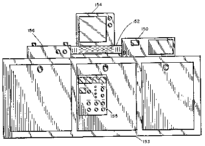
34 Figs. 1 and la together show a structural
''~'`'~
~2~ 7
01 3b
02
03 schematic representation of the invention with most of the
04 more important elements shown therein, including a very
05 general representation of a three section cabinet containing
06 the laser generating means, the electronic ciruits and
07 controls therefor, and also shows the computer system
08 components;
09 Fig. 2 is a more detailed showing of the
generation of the laser beam, the means for measuring the
ll intensity of the beam, and shutter means for blocking the
12 beam Erom entering the ~urnace portion of the system when
13 desired;
14 Fig. 3 shows a typical triangularly shaped path
of the laser beam as it appears on the moving crystal wafer;
16 Fig. ~ is a table relating the main translation
17 table input paeameters to table speed;
18 Flg. 5 is a table relating the scanning mirror
l9 input. parameter to scan Ere~uenc~;
Fig. 6 shows an example oE a selected group oE
2L parameters:
22 Fig. 7 ls a chart showlng the relation between
23 laser power versus cureent control dial setting; and
24 ~ig. 8 shows the Menu Table of the computer
~5 portion o~ the s~stetn.
26
27 DETAILED DESCRIPTION OF THE INVENTION
28 ~ block diagram of the s~stem is shown in Figure
29 la. The laser beam 10 is directed through three beam
steering mirrors 102, 10~, and 106 to the gelvanometer
31 112-driven scan mirror 108 which is mounted within the
32 stepper motor 110-driven linear translation stage 126. The
33 scan mirror 108 directs the laser beam 100 through a
~2~
focusing lens 114 that focu~es the laser beam down to 8
spot 120 on the sample curface 122 of crystal ~afer 116.
The an~le that the beam 100 ~trikes the ourf~ce 122 csn
be changed by remounting the scsn mirror 108 and lens
114 at Yarious predrilled holes (not shown) within the
translation ~tage 126. The change in angle is important
to incresse laser power absorption by the cr~stsl sample
by implnging at or near the Bre~ster angle.
The lens 114 used to focus the beam 100 is mounted
on a small, stepper motor 130-driYen linear-translstion
stage 113 to allow control o~er the focused beam spot
120 size. By mo~ing the ata8e 113 the beam can be
defocused to heat a larger area of the wsfer 116 at any
one instant in tlme. The laser beam 100 at the lens 114
ls about 1 cm in diameter and the lens 114 csn haYe a
focal length of 24.5 cm. By measurement, the sharpest
focus of the la3er beam gi~es a spot 120 about 0.5 mm
RMS in diameter, ~hich is larger than a perfect
dlffraction limited spot by about a factor of t~o.
Oppo~ite the lens 114 to the ri8ht in Fig. lu is a
~econd stepper motor 132-driven linear stage 159. It is
u~ed either to hold an absorber 134 to trap the
re1ected beam 100 or to posltlon ~ concave mirror ~in
place of absorber 134) to focus the beam lOO back down
to the ~urface 122 to increase the energy absorbed in
the sample 116. When a concave mirror is used as
element 134 it is driven by stepper motor 13~ (via
translation stage 159) to produce a spot that scans back
and forth 180~out of phase with the original spot 120,
but in the same zone area.
A Yacuum chamber 140 holds the sample 116. The
chamber 140 i~ designed to allow the beam 100 to enter
at 45 or at normal incitence ~ia 3alt ~indow~ 142, 144,
snd 146. The normal mode of operstion 1B to send the
.
~2~
laser be~m in st 45 and to view the sample through the
top salt vlndow 14~ with a pyrometer 148 for temperature
messurements. The ~acuu~ chamber 140 does not ~o~e snd
the ~mall salt window~ 142 and 146 allow onl~ a 2 cm
S scan distance sn the sample 116.
It should be noted that, if desired, the glassed-in
port 129 can be used to observe the bottom surface of
the crystal wafer sample 116. If desired the first
pyronometer 148 or a second pyronometer 148a can be
mounted a~ shown to view the sample 116 through port 129
by means of reflection off fold mirror 143.
A v~cuum ion pumping ~ystem 135 i8 connected to
vacuum ch~mber 140 through tube 137 and aligned orifices
in flanges 133 and 131. The clrystal wafer 116 is placed
lS over an orifice 139 in the middle plate 151.
The Pyronometer 148 field of view i8 linearly
movable both in the X and Y coordinfltes by two
galvanometers whlch drive ~irror 147 (galvanometers not
shown but ~imilar to galYanometer 112) to measure the
heat Benernted at sny given desired spot ~nd at any
de~ired t~me during thc scanning period of the laser
beam.
The entire n~embly 126, lncluding galvanometer
112, focuslng lens 11~ ~nd its carrier translation ~ta8e
113, ~pherical mirror (or absorb0r) 134, and its carrier
stage 1S9, stepper motor drives 130 and 132, and
pyronometer 1~8 and its ~alvonometer driven mirror 147
are all mo~able together in unlson on threaded carrier
shaft 125 which iB driven by statio.nary stepper motor
drive 110. Rods 123 and 121 function to guide the
movement of stage 126 in a uniform, translational
~otion,
The triangular pattern of the laser beam psth on
~he crystal wafer 116 is a result of the constant
velocity, linear motion of the trsnslation stage 126 in
a horizontal direction ~ in the plane of Fig. la and
~2~
with it the same component of constant velocity linear
motion of the laser beam spot on the wafer 116, combined
with the simultaneou~ linear back and forth scanning
motion of the l~ser besm 100 resulting from the movement
of the galvonometer driven mirror 108 ~hich is
repetieious over a single line that ~5 Rtationsry with
respect to the translation atage 126 in the direction X
in which it i9 moving~ bnt perpendicular to the
direction X.
All parts of the scanning syste~ are controlled by
a microprocessor control computer 150 of Fig. 1. The
computer 150, accessible by keyboard 152, can be A
single board system bssed on a Motorola 6809
microproce~sor, and can use the FLEX operating system.
XBASIC can be used for most of the programming but some
routines are preferably written in assembly language.
The sy~tem has a resl time clock, analog to digital
(A/D) circuits to re~d the laser power meter 188 of Fig.
2 and drivers for the stepper motors, scan ~irrors, and
la~er b~am ~hutter 182 (Fig, 2), Perlpherals can
include a keyboard 152, ~ CUT display 154, a printer
156, nnd a dual 5,~5 double ~ided, double density floppy
d~sc drives tnot ~huwn in Fig. 1). The ma~or components
of thc s~t~m were obtained, nssembled, and supplied by
Penn Res~arch Corporation (PRC) o~ Kennesaw, Georgiu.
Fi8~ 2 show generally how the C0~ laser beam 100
ig 8ener~ted and fits into the overall system. A laser
tube 170 powered by laser power supply 176 i8 positioned
between a rear cavity mirror 174 and a front cavity
mirror 172, between which the laser ~eam is reflected
back and forth and generates itself. Both cavity
mirrors 174 and 172, however, will pa99 come of the
laser beam with front cavity mirror 172 passing more of
the laser beam than rear caYity mirror 174.
That portion of the 8enerated laser beam passin~
through fron~ cavity ~irror 172 will enter the laser
5~
furnace ~ssembly 192 of Fig. ~ when the lead shutter
182 is in its open position 184. A smaller amount of
the laser beam will enter power meter 188 to indicate
the laser beam intensity or power. Both laser power
meter 188 ~nd shutter 182 are controlled by computor 150
8S iS the laser furnace assembly 192 and the laser power
supply 176. The laser tube coolant control 178 and the
gas mixture control lBO are controlled by dials and
meters on the control panel 155 of Fig. 1 which is
positioned on the front of the cabinet 153 of Fig. 1.
Two ma~or experiments were performed to verify the
operation of the equipment shown in Figso 1~ la and 2.
One of these experiments used silicon as the
semiconductor material and the second experiment used a
nickel based super allow (MARM-246) as a metallic
crystal. Silicon was selected because its properties
were well known and much experimental data was available
rel~ting to the u~e of csrbon dioxide lasers to melt or
cut the ~ilicon mnterial~ ~ickel ba~ed super alloys
were of particular intere~t becuase of their importance
in rocket engine~ and at hi8h temperatures in general.
In preparu~ion for the experiments the carbon
dioxide l~ser system o Fi8s. 1 snd la with the laser
beam 100 under computer control wns placed into
operation. The laser beam 100 supplied over 50 wstts on
a sample surface focused to a spot a9 s~all as 0.5 mm.
The beam ~as linearly scanned at frequencies selectively
rangin~ from 0.04 to 60 Hz~ The width of the scan was
made expandable up to 1.8 cm and the ~can zone mo~ed at
speed ran8ing from 0.001 to 25 cm/sec. The basic goals
for the beam control were thus achieved.
Initial attempts to melt the silicon wafer re~ealed
a maJor problem with the s~stem which was determined to
be an excessive loss of laser power through the optical
train. All of the initisl beam alignment had been
previously done at low power settings and it was not at
first realized that when the laser power was increased
the besm diameter also increased. The scsn mirror l08
of Fig. la has a circular shaped graphite absorber 107
positioned to trap the laser beam lO0 if the slignment
~oves. Becsuse of the doughnut shaped mode assumed by
the laser when the beam diameter increased the grsphite
absorber 107 blocked the outside diameter thereof and
the power transmitted to the sample actuall~ decreased.
When the situation was finally realized, the hole in the
graphite absorber 107 was increased and a larger scan
mirror 108 W8S placed on galvanometer 112 of Fig. 1~
With that remedy the silicon wafers were melted for the
first time. It fact, it was disco~ered vèry quickly
that any power setting oYer 50 watts heated up the
sample too rapidly and the silicon wafer shattered.
Measurements of the optical system tr~nsmission
efficlency to determine the maximum power that could be
placed on the silicon wafer sample re~ealed that all the
mirrors reflected more than 99 percent of their received
power but that about ~0 percent of the laser power was
lost at the focusing lens 1l4 due to surface
reflection, Thereore, at any reading of the power
me~er 188 ~i8. 2) ~h~ actual power on ~he surface 122
of cryut~l waar ll~ wa~ ao p~rcon~
~S The ~licon w~er sample~ used in the e~per~ments
were ~nte8rated circuit wafers 24 cm in d~ameter and 13
mils thlck. At a 45 nngle of incidence the wafers
transmltted 50 percent of the incident energy and
reflected 37.5 percent thereof, lea~ing 12.5 percent to
actually heat up the crystal wafer msterial, As the
temperature of the sample increased, the absorption
increased. The data recorded agreed very ~ell with
published data. At power sett~ngs of 40 v~tts, melt
zones 5 mm wide were generated and mo~ed slong the
sample. The main translation stage 126 Yelocity had ~o
be slower than 2 mm/sec or ~he melt zone could not be
~5~37
01 9
02 maintained.
03 Attempts to melt the nickel/based supper alloy
04 metal crystals were unsuccessful. The laser power of the
05 particular form of the invention was insu-fficient enough
06 to melt the size sample available. These samples were
07 rods about 5 mm in diameter and 49 mm long. The high
08 reflectivity of the metal indicated that more than a
09 hundred watts might be required to initiate the melt.
In opera-ting the system the following procedures
11 were used. The carbon dioxide laser beam was generated as
12 shown in Fig. 2. However, the specifics oE the procedures
13 for generating the carbon dioxide type lasers used herein
14 are well known in the art and will not be described herein
other than in the general manner shown in Fig. 2.
16 ReEerenc~ is made to the following publications for
17 further information relating to CO2 lasers: (1) "American
18 Institute o~E Phyqics Manclboolc", Dwight E. Gray,
19 Coordinating ~ditor, Mc~raw-MilL Book Company, Colonial
Press, N~, Thirc1 E.clltLon L972, Sectlon 6, Page 326 and ~2)
2l "~ntrocl~lctLon to T.,aser Phy~ics", ~ela A. ~engyel,
22 ProEe~sor, ~an ~'errlarlclo Valley ~tate College, John WLley
23 ~n~ Son~, Inc., ~w ~ork, 1~66, Chapter V, Page 209, to
2~ which the reader 1~ reerred.
Once the laser is on and operating the shutter 182
26 (Fig. 2) ha~ to be switched open to poæition 184 to allow
27 the beam to reach the scanning optics, as shown in Fig.
28 la. When the shutter 182 i9 closed the laser beam 100 is
29 blocked by a metal trap which is shutter 182. Even at
full laser power the shutter 182 will trap the laser beam
31 100 continuously without overheating. The power meter 188
32 (Fig. 2) is located immediately behind the rear cavity
33 mirror 174 and operates by measuring the small percentage
34 of the laser beam transmitted by the rear cavity mirror
174. Therefore, the power meter 188 will read the correct
36 power even when the shutter 182 is
~65~
closed.
The laser power can be optimized by ad~usting the
ca~ity mirrors 174 and 172 at each end of the laser 170
by rotating each of the two mirrors ~bout two
orthogon~l axis by suitable means (not 8hown). The
maximum power is obtained when the ca~ity mirrors are
set for 8 "doughnut" mode (TEMOl) of operstion of the
laser be~m. Thermal image pl~tes can be manually placed
in the path of the laser beam to locate the invisible
carbon dioxide laser beam and determine when the best
alignment i8 achieved. A small ultra-~iolet lamp is
used to illuminate the thermal image plates causing them
to fluoresce. The laser beam will cause the fluorescence
to cease and appear as a dark image on the thermal image
plates.
To operate the computer 150 (Fig. 1), the power is
turned on ~nd a reset button ~not shown) i8 pushed. The
computer 150 i8 then instructed to load the operating
~ystem. When the operating system ls loaded the
computer will ~e the time and date and display th FLEX
~ystem READY messa8e. The control prosram i8 written in
baslc ~o the basic languQge must be loaded. The
operntor load~ basic by typing "XBASIC" and hitting the
cnrria~e re~urn key. When the READY message is
displayed the actual control program ~s loaded by typing
the code word "load NASA3" and a8a~n hitting the
carria~e return key. Once the READY ~es6sge i8 again
dlsplayed the operstor can run the control program by
typing "RUN" and once again hitting the carriage return
key.
The control program first displays a Menu Option
table. An example is shown in Fig. 8, A~ option is
~elected by entering the number below each ~election~
To mske an experimental run the psrameters must first
be entered and stored in a data table. An example of a
typical data table i~ shown in Fi8. 6. The d~ta table
i5~7
11
build option sllows the operator to generate a new data
table vhenever desirable. The computer will ask for a
name for the data file and than ask for each parameter
one at a time. After the ~alues ~re entered the
computer will ask if the file is to be saYed or printed.
When ~he file is sa~ed, the menu option ~ill again be
displayed and the operator can select the Execute mode
for the table option, The computer will ask for the
file name to run and then ask if any changes to the
parameter3 are required. B~ entering the letter beside
the parameter the operator can change the table before
running it. There ~s also an option to sa~e or print
the parameters as they are now on the screen. The
computer will automatically store any table on disc
after the co~mand is actually given to run the table.
The disc file i8 called LASTRUN and i8 insurance that
the last ran data can be retrieved. I
The example of the typicsl data selected by the
operator under tha TABLEBUILD MODE o the MENU of Fig.
8, as shown in Fig, 6I will now be discussed in some
dctail.
The assembly ~ta8e 126 ~Fig. la ) ~tart and stop
posltions in rows A and B of Fi8. 6 are in centimeters
as ar~ the po~itions o th~ len~ 114 8ta8e in row D and
2$ the nbsorber ~or mirror) 134 in row E. The given
measu~ements of the assembly stage start and stop
positlons are relative to the zero drlve position of
stepper motor drlve 110, l.e., the extreme left
position, and the measurements of the positions of the
len~ 114 and mirror 134 stages are relative to zero left
and right extreme positions of stepper motor dri~es 130
and 132, respecti~ely.
The assembly stage 126 ~elocity of row C in Fig. 6
is in milliseconds which i3 represented and translated
by the parameter 100 set in a specific memory location
in the computer RAM. The primary scanner 108 (Flgo 18)
~2~i5~
12
frequency and amplitude are al~o represented by
parameter nu~bers which are set in designated memory
locations in the computer RAM and translated by the
computer into time frequency and amplitude of the
S galvanometer 112.
Rows H, I, J, and K represent the frequencies and
nmplitudeq of ~wo gal~anometers (not sho~n) that can be
employed to drive the folding mirror 147 along
coordinate X and Y sxis in much the same vay as
gal~anometer 112 driYes the scanning mirror 108.
The two additional galvanometers used ~o ~rive
mirror 147 would be under control of the system computer
150 and would permit the pyronome~er 148 to monitor the
heat on ~ny spot on the crystal wafer surface.
The numerals "1'l in column II of rows H through K
are purely arbitrary and meaningless parameters. IP the
two additional galvanometers for driving mirror 147 of
Fig, 1 were actually used, meaningful parameters would
be placed ln rows R through K of column II.
~0 In row L the initial wait or melt zone i~ selected
as 32000, which represents the number o dummy scan
loop~ tha~ the computcr make~ to nllow She ~one on the
crysta~ w~er bein8 scanned to melt before the ~ssemblr
stagc 1~6 be8in~ to move. The number 3~000 i8 a
parame~er repre5~nting a gl~en time interval and is set
into a given memory position in RAM by the operator.
Row M represents the number of times the ~el~ (scan)
zone will be moved through the crystal wafer sample.
In Fi8. 4 there is ~hown the relationship between
ten choices of vslues in column II ranging from 50 to
32000 ~nd the corresponding ~elocity of the staBe 126
(Fig. la). The value 50, for example, placed in 8
preselected memory location of the computer, results in
a velocity of 5.00 millimeters per second (~m/sec) of
translation stage 126 (Fig. 1). ,The value 2000 (column
II, row 6) of Fi8. 6 r~sults in 8 ~elocity of 0.171
1 3
mm/sec of stage 126. The start and s~op positions of
stage 126 are predetermined by the Yalues selected for
rows A cnd B of Fi8- ~-
Fig. 5 shows the relation of the scan ~irror input
par~meter entered in row F of the data table of Fig. 6,to the actusl scanning frequency in Hz of the scanning
mirror 108 (Fig. 1). Thus, for example, in Fig. 5 the
scan mirror input parameter value of 1000, in row 11,
represents an actual scanning frequency of 1,25 Hz. The
scan mirror input parameter value 1000 is preselected by
the operator and placed in row F of the data bank of
Fig. 6. As mentioned abo~e in connection with Fig. 6,
the amplitude of the primary scanner mirror 108 is
~ represented by the parameter 500,
The sequence of events that happen after the
instruction to execute the ~UN the control progrsm is
entered i~ ted below:
1) The lens and reflector stages are posi~ioned to
the locstions specifled ln the data table. Both motors
appear to run nt the same time.
2) Th~ main translation stage 126 i9 positioned to
the zaro reference point, i.e., dr~ven to the extreme
left po~i~ion in Flg. la.
3) The ~can m~rror lQ8 i~ ~tarted. (The shutter is
not opcned.)
4) The main translation sta~e 126 i~ moved to
specified ~tart position.
5) The shutter 182 is opened and the laser beam is
allowed to strike the surface 122 of ~afer sample 116.
6) The main translation stage 126 is held
6tstionary for the 6pecified wa$t period.
7) The main translation sts8e 126 stsrts to move
and dri~es to the final position specified in row B of
Fig. 6.
8) The shutter lB2 iB closed~
9) The translational stage 126 ~s dri~en back to
~6~
14
the zero reference position if it is the last run or to
the melt zone start location if additional cycles are
specified.
10) The cycle i8 repested the specifiad number of
times ~pecified in row M of Fig. 6.
A gal~anometer 112 ls used to drive the scan m~rror
108 instead of an oscillating band so that the linear
triangularly shaped sweep of Fig. 3 caD be producedO
The waYeform generated by the computer is a triangularly
shaped wsve and the galvanometer 112 will faithfully
follow the signal up to ~bout 60 Hz. Abo~e 60 Hz the
scan becomes more snd more sinewsve shaped as the
frequency is incressed. Fig. 3 shows the scan pattern
achieved onto crystal wsfer 116 below 60 Hz.
The laser power i~ variably controlled by changing
the current flowing through a current control variable
modulator (not shown). The actual power obtained for any
one setting varies from daylto day for reasons which
hsve not been established but i8 probably related to the
8as mixture in which the laser is 8enerated and
temperature conditions. Fig. 7 show~ two curves which
were obtained during attempts to calibrate the dial
settinBs of the meters ~not ~hown) indica~ing the la~er
c~rrent and re~u~tin8 laser power. It is recommended
that n di01 ~ettin8 le~s th~n 20 not be used because
dial aettin8a lower ~han 20 produre hi8h voltages across
the laser tube 170 (Fig. 2) which may be bigh enough to
break down the insulators that isolate the tube 170 from
ground. Laser power settings sbove 80 on the dial are
30 8190 not recommended due to the high currents through
the tube 170. However~ although the laqer is rated at
85 ~atts it actually has a maximum power rangin8 from 70
up to 95 watts. Obviously other laser constructions csn
be employed ~hich will provide a larger range of power
and psrticulsrly 9 substantiallg greater maximum power
setting.
Control of the laser power may be accomplished by
manual adjustment as described above or by automatic,
real-t~me control through computer 150, using feedback
signals from pyrometer 148 and from laser power me~ter
05 188 or from computer memory using previously programmed
parameter tables.
It is to be understood ~hat the form o~f the
invention described and claimed herein is but one
preferred emodiment thereof and that other embodiments
of different parameters will be apparent to one of
ordinary skill in the art.