Note : Les descriptions sont présentées dans la langue officielle dans laquelle elles ont été soumises.
-- 1 --
A Phased Array Transmitter
This invention relates to a phased array transmitter
or receiver and is particularly applicable to a radar
system. It could, howeYer also be app~ied to an acoustic
5 system e.g. sonar.
In a phased array transmitter there are a number of
antenna elements and means for controlling the phase of
energy fed to or received from each elemen-t in such a way
as to give the antenna a required directional sensitivity
pattern. This may for example be a single beam or a
number of beams and the beam or beams can be made to
change direction if required. The phase control is
conventionally obtained by passing energy to be
transmitted from a common source through separate branch
lines containing phase shifters. The phase shifters
usually comprise switches which divert the energy through
one or more o a number of lines having different lengths
so as to produce the required phase shift.
To enable the prior art to be described with the aid
" of a diagram, the igures of drawings will first be listed.
Fig. 1 is a block diagram of a prior art arrangement;
Fig. 2 is a block diagram of part of a transmitter
constructed in accordance with a first aspect of the
invention; and
Fig. 3 shows another embodiment, employing additional
aspects of the invention, this also being used for
transmission only.
~5~
In a phased array receiver the same type of phase
shifter may be used, with signals from the antenna elements
being passed through respective phase shifters and then
combined.
A limitation of the conventional techniques described
above is that the phase shifters are able to produce only
discrete phase changes between particular values.
Another technique which has been given theoretical
consideration (e~g. as described in UK patent
1(3 specification 2056781) is to employ phase lock loops to
control the phases at respective antenna elements. Such
an arrangement is shown in Fig. 1.
~ reference frequency which is common to all the
antenna elements is applied to a mixer which provides an
average output voltage which is dependent on the phase
difference between its two inputs. This is applied (via
an adder which will be described later) to the input of a
VCO whose output passes to the antenna element and also
passes through optional dividers or frequency converters
?d back to the phase comparator. The action of the loop is
to lock the frequency of the VCO to the reference
frequency. In the system of Fig. 1 as described so far
the phase of the VCO relative to the reference frequency
depends on many factors such as the values of components
~5 within the phase comparator and VCO, which may not be
accurately known.
'~!
-- 3
A method o~ con~rolliny the phase, which has been
considered is to add an offset voltage to the output of
the phase comparator before it passes to the VCO as shown
in Fig. 1, different offsets being applied for different
antenna elements. The offset volta~e causes the loop to
re-stabilize at a different point on the phase comparator's
characteristic curve, which different point corresponds to
a different phase relationship between its inputs; and
there~ore the VCO phase relative to the reference frequency
lo has been changedO There are several problems with this
tecllnique O
(i) Tl.e phase before application of the Gffset may
not be accurately known as mentioned previously
and therefore the phase after application of the
offset may not accurately be known either.
(ii) The phase comparator will only be usable oqer a
limited range where it is reasonably linear.
This limits the range of phase control
obtainable.
(iii) The dependence of the VCO phase on the phase
control voltage depends on the characteristics
of the phase comparator, which may not be
accurately known.
This invention provides a phased array transmitter
comprising: a reference oscillator, an array of antenna
elements; for each element a phase lock loop comprising a
~5~
-- 4
voltage controlled oscillator whose output is connected to
the associated element, and a phase comparator arranged to
compare a signal derived from the output of the voltage
controlled oscillator with a signal derived from the
reference oscillator, and control means for controlling
the phases at which the oscillators lock; characterised in
that the control means comprises a circuit located between
the phase comparator and the voltage controlled oscillator
which circuit perfor~s a sum-and-integrate function on
1(~ voltages received from (i) the phase comparator and (ii) a
phase control input to the loop.
Because of the use of the aforementioned sum-and-
integrate function the aforementioned problems (i) can be
overcome because the phase of the oscillator before
application of the phase control input is accurately known.
It is accurately known because the output voltage of the
phase comparator is accurately defined as equal to a
reference voltage of the sum-and-integrate circuit.
Furthermore by employing a phase comparator using digital
components, instead of a mixer which is conventional, the
problems ii and iii can also be overcome. This is because
digital phase comparators can provide a linear
characteristic over 360.
According to another aspect of the invention there is
~5 provided a phased array transmitter comprising: a
re~erence oscillator, an array of antenna elements; for
æ~ s
-- 5 --
each element a phase lock loop comprising a voltage
controlled oscillator whose output is connected to the
associated element, and a phase comparator arranged to
compare a signal derived from the output of the voltage
controlled oscillator with a signal derived from the
reference oscillator, and control means for controllin~
the phases at which oscillators lock; characterised by
means for processing the output of the voltage controlled
oscillator to reduce the frequency thereof; a counter for
counting cycles of the reference oscillator, a digital
word comparator for comparing the content of the counter
with a phase control input word to provide a pulse, when
its inpu~s are equal, the phase comparator being arranged
to compare t'ne phase of the reduced frequency signal with
l~ the phase of the pulses at the output of the comparator.
By employing this second aspect of the invention the
problem mentioned at ii above can be removed because the
phase comparator always stabilizes with the same phase
difference between its inputs. Also problem iii can be
avoided because now the VCO phase no longer depends on the
phase comparator characteristic and is instead accurately
determined by the digital counter and comparator circuit.
The sample and hold circuit performs the function of
mixing the VCO frequency with a harmonic oE the reference
frequency which controls it in order to convert a high
~e.g. microwave) VCO frequency to lower frequency suitable
~L~6~
-- 6 --
for digital processing.
Whilst a sample and hold circuit i5 preferred it would
be possible instead to use a mixer or a divider.
In a preferred embodiment oE the invention both
aspects of the invention as defined above can be employed.
In such an arrangement the second aspect of the inven~ion
can be used tp provide a stepwise adjustment of phase and
the first aspect to give a fine adjustment between steps.
This will become apparent from the following description
but it is emphasized that either aspect can be used alone.
Two ways of performing the invention will now be
descri~ed by way of example with reference to Figs. 2 and
3 of the accompanying drawings in which :-
~eferring to Figure 2 input data is applied on line 1
to a beam steering device 2. The input data defines at
any time the required directional characteristics of an
antenna. The beam steerer 2 produces, in response to the
data applied at 1, phase control signals on lines 30
These signals are analogue voltage values which control
~0 proportionally the phases of energy applied to individual
elements of the antenna.
In the drawing only three lines 3 for three respective
elements are shown but it is to be understood that there
are in fact many more.
Each phase control signal on a line 3, togekher with
a reference signal 4 from a fixed frequency oscillator 6
~2~86~
- 6a -
is passed to a phase lock loop 7. One such phase lock loop
is provided for each antenna elemen~ 5. They are all the
same and so only one is illustrated in detail. This
comprises a voltage controlled oscillator 7~ whose output
is split between the antenna element 5 and a phase
sensitive detector 7b where it is compared with the phase
of the signal from the reference oscillator 6 to produce a
voltage wtlose mean value represents the relative phase of
oscillators 6 and 7A. The output of the phase comparator
~;26586S
is applied to 011(? input oE a sum-and-integrate circuit 7C
whose other input is a voltage on a line 3. The circuit 7C
may comprise a diEEerential amplifier with ~eedback
connection as described in the book "Analysis and Design
o~ Electronic Circuits page 438-441 by P.M. Chirlian,
McGraw Hill 1965. The output of circuit 7C is a voltage
which controls the oscillator 7A with correct polarity to
cause the loop to stabilise. In this way the phase of the
oscillator 7A is oEEset from the re~erence oscillator 6 by
an amount dictated by the voltage on line 3. The
desirable feature of accurate proportionality of phase
ofEset to voltage is obtainable by using first an
integrator 7C with very high gain at d.c. and second a
phase comparator with a wide linear range.
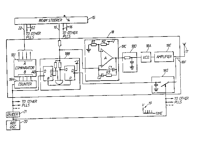
lS Fig. 3 is a block diagram oE another transmitter
constructed in accr.rdanc~ with the invention. Data is
applied on line 14 to a beam steering device lS which
produces phase control signals on lines 16, one Eor each
oE a large number oE antenna elements oE which only one is
7~ shown at 17.
Each antenna element has a phase control circuit 18
~only une being shown) which receives a phase control
signal From the appr~priate line 16. The circuit 18
c~ntains a voltage contl-olled oscillatol~ 18A, a phase
sensitive detector 18B and an integl-ator l8C similal- in
~unction to the components 7A, 7B and 7c Or ~ig. 1.
Inte~l-atol- 18c compl-ises a dirrelen~ial amplifi~r A with
3L%65E~
resistors Rl and R2 to provide a rc~erence voltage between
the binary high and low levels o~ the logic circuits in
18B, and components Cl, C2, R3 which are chosen ~or loop
stability in accordance with conventional design methods.
The phase sensitive detector 18B is a digital type which
compares the times of signal swings at its two inputs and
delivers a pulse to the integrator 18C of duration equal
to the delay between the said swings and o~ polarity
dependent on which swing arrived ~irst. The circuit 18B
1~ can consist oE two D-type ~lip-~lops (7474) and one NAND
gate (7400) connected as shown, where the numbers o~
standard TTL components described in the book: "The TTL
Data Book ~or Design Engineers," cc - 411 1975, Texas
Instruments are given in brackets.
A low-pass ~ilter 18D reduces unwanted phase
modulation of the oscillator 18A caused by incomplete
smoothing of phase detector pulses by integrator 18C. An
ampli~ier 18E provides the required transmit power to
antenna element 17.
A sample oE the output signal is obtained by a
directional coupler 18F and is ~ed to a sample-and-hold
circuit 18G which is driven by pulses 19 fl-om a reference
oscillator 20 similar in function to the oscillator 6 o~
Fig. 1. The ef~ect o~ circuit 18G is to convel-t the
output frequency to a lower [reqllency at which circuits
18l3, 18H and 18I can Euncti~Jn and i~ may ~e r(~gal~ded as a
l~ssless mixel-. ReEel~(~nce osci]lal(,l 20 <-~ls~ reeds a
~2Ç;5 !365
g
divider 21 whose output is distributed ~o all the loops 18
where it serves as a clock input to a digital counter 18H
(74161) and to the phase sensitive detector 18B which
receives a reference pulse from a digital
comparator 18I (7485) once in every cycle oE counter 18H
when the state o~ counter 18H equals a digital word sent
by beam steerer 15 on lines 22 each oE which has four
conductors.
This arrangement provides two means o~ controlling
the phase o~ energy at antenna element 17, namely by a
voltage on a line 15 which causes a proportional phase
change and by a four bit digital word on a line 22 which
gives a choice o~ 16 discrete phases. This number can be
varied at will by design o~ counter 18H and comparator
18I. The said two means can be used separately or
together.
The positioning of the amplifier l9E within the phase
lock loop, rather than between the phase lock loop and the
antenna element is advantageous because it eliminates
~0 problems which would otherwise occur as a result oE
unpredictable phase shi~ts within the ampliFiers.
Phase lock loops like those shown at 7 in Fig. 2 or
18 in Fig. 3 can be used as local oscillatol-s in phased
anl-ay l-eceivers to achieve the same beneEits as have been
descl~ibed ~ol- transmit~c?rs.