Note : Les descriptions sont présentées dans la langue officielle dans laquelle elles ont été soumises.
~26688~
SPECIFICATION
OUTPUT POWER CONTROL CIRCUIT FOR
A MOBILE RADIO APPARATUS
BACKGROUND OF THE INVENTION
The present invention relates to an output power
control circuit for controlling the output level of a RF
(radio frequency) signal amplifier employed in a mobile
radio apparatus such as a mobile telephone and, more
specifically, to an output power control circuit which
supplies output power level control fiignals to a RF signal
amplifier to determine the output power level of the RF
fiignal amplifier selectively.
A mobile radio apparatus must be formed in a compact
construction so that the mobile radio apparatus can be
placed in a small space in an automobile or so that the
mobile radio apparatus is handy for carrying about.
Accordingly, the mobile radio apparatus employs compact
electronic parts to reduce the size of the casing thereof.
Reduction infiize of the casing entails a problem that the
internal temperature of the mobile radio apparatus,
namely, the temperature inside the casing, is caused to
rise to an upper limit temperature, for example, 85C,
guaranteeing the rated performance of the mobile radio
apparatus in a short time by the heat generated by the
electronic components, mainly by the heat generated by an
i266885
RF signal amplifier.
Particularly, when the RF fiignal amplifier provides
RF fiignalfi of a high power level, for example, three
watts, the RF signal amplifier generates heat at a high
rate, which further reduces the time in which the internal
temperature of the casing rises to a predetermined upper
limit temperature.
Incidentally, the output power level of the RF
amplifier is maintained at a stable output power level by
an automatic power control circuit (hereinafter
abbreviated afi an "APC" circuit).
As described in detail in U.S. Patent Nos. 4,523,155
and 4,602,218, the conventional APC circuit maintains the
output power level of the RF signal amplifier at one of a
plurality of output power levelfi which are selected by a
plurality of level control signalfi, namely, parallel input
bit pattern~, and level control fiignals to be supplied to
the APC circuit are fiet according to power fietting command
fiignals tranfimitted through a control channel or a voice
channel by a master ~tation. Accordingly, the mobile
radio apparatufi ifi unable to lower the output power level
thereof independently even when the internal temperature
of the cafiing thereof reach the predetermined upper limit
temperature. In such a cafie, the mobile radio apparatus
disconnects the power fiource automatically to interrupt
the tranfimififiion of RF signals, namely, to prevent
communication, until the internal temperature dropfi below
lZ66885
the upper limit temperature.
SUMMARY OF THE INVENTION
Accordingly, it is an object of the present invention
to provide an output power control circuit for a compact
mobile radio apparatus, capable of extending the available
time of continuoufi communication by reducing the rising
rate of the internal temperature of the casing of the
mobile radio apparatus.
It is further object of the prefient invention to
provide an output power control circuit for a mobile radio
apparatus, capable of generating level control signals for
controlling the output power level of the RF signal
amplifier without spoiling the dependency on power level
etting co0mand signalfi given thereto by a master fitation.
According to one afipect of the prefient invention, an
output power control circuit for a mobile radio apparatus
having a casing, an APC circuit and a RF fiignal amplifier,
provided in the casing of the mobile radio apparatus and
adapted to apply level control fiignalfi to the APC circuit
for maintaining the magnitude of the output RF fiignal of
the RF signal amplifier at one of a plurality of output
power level~ correfiponding to the level control signalfi,
which comprifies:
a receiver which receives RF signals transmitted by a
maæter station and detects power level setting command
fiignal~ included in the RF signalfi;
~26688~i
a temperature ~en~ing circuit which detects the
internal temperature of the casing and provides a power
reduction signal upon the detection of the internal
temperature exceeding a predetermined temperature; and
a logic circuit which receives the power level
setting command signal from the receiver, generates a
level control signal for determining an output power level
corresponding to the power level setting command signal,
and generates a level control signal for determining an
output power level which is lower than that specified by
the power level setting command signal upon the reception
of a power reduction signal from the temperature sensing
circuit.
BRIEF DESCRIPTION OF THE DRAWINGS
Fig. 1 is a block diagram of an output power control
circuit for a mobile radio apparatus, in a preferred
embodiment, according to the present invention;
Figs. 2(a), 2(b), 2(c) and 2(d) are graphs showing
the variation of the internal temperature of the casing of
a mobile radio apparatu~ with time, the variation of
voltage applied to the plus input terminal of an amplifier
according to the internal temperature with time, the
variation of the output voltage of the amplifier according
to the voltage applied to the plus input terminal of the
same with time, and the variation of the output power
level of an RF signal amplifier according to the internal
~26688~i
temperature with time, respectively;
Fig. 3 is a flowchart showing steps of a control
program to be executed ~y a logic circuit employed in the
output power control circuit of Fig. 1; and
Fig. 4 is a block diagram showing in detail a logic
circui~ according to the present invention.
DETAILED DESCRIPTION OF THE PREFERRED EMBODIMENT
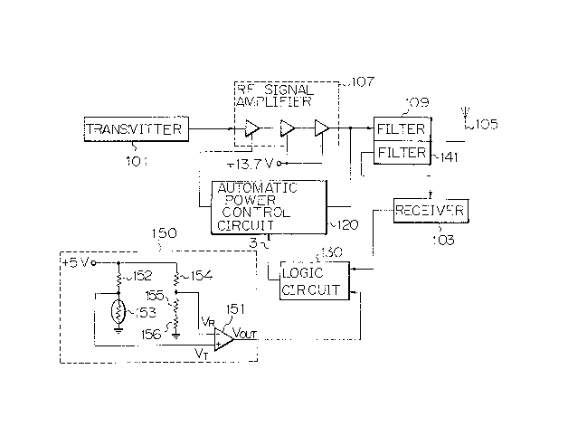
Fig. 1 illustrates a mobile radio apparatus
incorporating an output power control circuit, in a
preferred embodiment, according to the present invention.
The mobile radio apparatus has a conventional transmitter
101, a conventional receiver 103 and a conventional
antenna 105. The transmitter 101 feeds RF (radio
frequency) signals to a conventional RF signal amplifier
~107. The RF signal amplifier 107 amplifies the input RF
signals and suppliefi output RF signals, namely, amplified
input RF signals, through a conventional bandpass filter
109 to the antenna l05. The output power level of the RF
fiignal amplifier 107 is proportional to the voltage
supplied to the RF signal amplifier 107 by a conventional
automatic power control circuit 120 (hereinafter
abbreviated as an "APC circuit").
The APC circuit 120 detects the magnitude of the
output RF signal of the RF signal amplifier 107 to
maintain the output power level of the RF signal amplifier
at one of several different output power levels
1266885
corresponding to a plurality of level control signals. In
this embodiment, the level control signals are APC command
signals represented by 3-bit binary codes produced by a
logic circuit 130. The respective actual values of the
APC command signals respectively corresponding to eight
different output power levels are in the range of about
6.8 dBm to about 34.8 dBm.
When the logic circuit 130 produces an APC command
signal of "000", the output power level of the RF signal
amplifier 107 rises to the maximum output power level of
34.8 dBm. The output level of the RF signal amplifier
varies in an inverse proportion to the APC command signal.
That is, when the APC command signal increases by an
increment of "l" from "000" to "OOl", the output power
level of the RF signal amplifier 107 decreases by a
decrement of 4 dB from 34. 8 dBm to 30.8 dBm. When the
APC command signal is "1ll", the output power level of the
RF signal amplifier 107 is 6.8 dBm, which is the minimum
output power level of the RF signal amplifier 107.
The logic circuit 130 receives, through the antenna
105 and a conventional bandpass filter 141 and the
receiver 103, power setting (hereinafter abbreviated as
"PS") command signals transmitted through a control
channel or voice channel by a master station (not shown).
The PS command signal commands the logic circuit 130 to
set the magnitude of the output of the RF signal amplifier
107 at the corresponding output power level. The output
~2Ç;6885
terminal of a temperature sensing circuit 150 provided in
the casing of the mobile radio apparatus is connected to
the input terminal of the logic circuit 130 so as to apply
an output voltage Vout to the logic circuit 130.
The temperature sensing circuit 150 comprises an
operational amplifier 151, a resistor 152 having a value
of 4.7 kQ, a thermistor 153 having a value of l.9 kQat
75C, a resistor 154 having a value of 4.53 kQ, a resistor
155 having a value of 160Q and a resistor 156 having a
value of 1.6 kQ .
The plus input terminal of the operational amplifier
151 is connected through the resistor 152 to a voltage
source of +5V and is grounded through the thermistor 153.
The minus input terminal of the operational amplifier 151
is connected through the resistor 154 to the voltage
source and is grounded through the resistors 155 and 156.
As shown in Figs. 2(a) and 2(b), A fixed voltage VR
of approximately 1.4V is applied to the minus input
terminal of the operational amplifier 151 regardless of
the variation of the internal temperature of the casing.
A voltage VT is applied to the plus input terminal of the
operational amplifier 151. The voltage VT is higher than
the voltage VR when the internal temperature is the room
temperature, and is lower than the voltage VR when the
internal temperature is in a temperature range above
approximately 72.5C. As shown in Fig. 2(c), the output
voltage Vout of the operational amplifier 151 applied to
; ., _ _ . . . . .... . . - .- .. . .. . . . . . - -
~26688~;
the logic circuit 130 is 5V when the voltage VT is higher
than the voltage VRt and is OV when the voltage VT is
equal to or lower than the voltage VR.
The manner of operation of the logic circuit 130 will
be described hereinafter with reference to Fig. 3.
Upon the connection of the mobile radio apparatus to
the power source (not shown), the logic circuit 130
generates an APC command signal of "000" in Step 300.
Then, the logic circuit 130 receives a PS command signal
in Step 310. Upon the reception of the PS command signal,
the logic circuit 130 generates an APC command signal for
selecting an output power level corresponding to the PS
command signal for five seconds in Step 320 After the
passage of five seconds from the reception of the PS
command signal, the logic circuit 130 makes a decision
whether the output voltage Vout of the temperature sensing
circuit 150 is 5V in Step 330. When the output voltage
Vout is 5V, the logic circuit 130 generates an APC command
signal for selecting an output power level corresponding
to the PS command signal in Step 340, and then executes
Step 360.
When the determination in Step 330 is "No", namely,
when the output voltage Vout of the temperature sensing
ccccuit 150 is not 5V and hence is OV, the logic circuit
130 generates an APC command signal for selecting an
output power level nearest to an output power level lower
than the output power level corresponding to the PS
1 26'G88~;
command ~i~nal by 4 dB in Step 350, and then execute~; Step
360. In step 360, the logic circuit l30 determine~; if a
new PS comrnand ~ignal i~ received. If a new PS command
~ignal i~ fed to the logic circuit 130, then the logic
circuit ]30 execute~ Step 310 and, if not, the logic
circuit 130 execute~ Step 330.
A~ ~hown in Fig. 4, the logic circuit 130 compri~;es a
microprocessor 410 ~uch a~ an OKI type IC No. 80C85 and a
read-only memory 420 ~uch as a FUJITSU type era~able
programmable read-only memory No. MBC 27C256. The
microprocessor 410 receive~ a PS command ~ignal from the
receiver 103 and an output voltage Vout from the
temperature ~en~ing circuit 150 and applie~ an APC command
~ignal generated under the control of the read-only memory
420 to the APC circuit l20.
Thu~;, the logic circuit 130 control~ the output power
level of the RF signal amplifier 107 so a~ to be at 34.8
dBm when the internal temperature i~ lower than
approximately 72.5C, and ~o a~ to be at 30.4 dBm when the
internal temperature i~ approximately 72.5C or higher as
shown in Fig. 2(d), notwith~tanding the PS command ~ignal
reque~ting an output power level of 34.8 dBm.
Since the internal temperature oE a casing having a
volume of approximately 800 cm3 ri~e~ to approximately
72.5C or higher when the ambient temperature i~ in the
range of -30C to +60C and the output power level of the
RF ~ignal amplifier 107 i~ 34.8 dBm, the logic circuit 130
~26688~i
generates an APC command signal of "001" when the output
voltage Vout of the temperature ~en~ing circuit 150 i~ OV.