Note : Les descriptions sont présentées dans la langue officielle dans laquelle elles ont été soumises.
3~ so 2 o 9 6
BACKGROUND OF THE INVENTION
Field of the Invention:
This invention relatec generally to a high-vol.tage
stabilizing circult sultable for use in stabilizing a
high-voltage that is supplied to a ca-thode ray tube Erom a
flyback transformer and, particularly, a high-voltage
stabilizer for use with a flat-type cathode ray tube.
Descrl~tion of the Prior Art
It is known ~o utilize ~he horizontal output
transformer as the "flyback" transformer to develop the
high-voltage necessary for a cathode ray tube. This output
transformer typically provides both the high~vol-tage for the
cathode ray tube and also the horizontal scanning voltage.
In such output or flyback transformer high-voltage circuits,
it is known that the high-voltage output fluctuates
depending upon the total load in the transformer secondary,
which is a function of the resistance of the transformer
winding, the impedance~ of the restifier diode and bypass
capacitor, and other circuit elements forminy the switching
circuit. Additionally, the nigh voltage output wil.L also be
influenced by the cathode current of the cathode ray tube,
which varies in respon.se to the input video signal, because
the video output c.ircuit that receives the video signal is
powered by a low voltge also produced by the flyback
transformer. The resultant effect of ~hese hlgh-vol~ag~
fluc~uatiolls is that ~he position and size of the picture
formed on the cathode ray tube will vary. While such
pic~ure variations ar~ known, they have not been cri~ical,
because the variations in posi~ion and size of the picture
.,
I
~ 3~'' S02096
are not necessarily noticeable in a conventional ca-thode ray
tube. This is because the axial alignment of the guns
relative to the phosphorus screen do not cause a large shift
in the plcture for normal variations in the high-voltage
output~ Nevertheless, such position and size varia~ions of
the picture are quite conspicuous in a so-called flat-type
cathode ray tube, such as employed in currently available
miniature, personal television receivers~ This conspicuous
variation in size and position of the picture in such
flat-type ca~hode ray tubes is due to the relatively small
angle be ween the phosp'norus screen and the center axis of
the electron gun or guns of the tube, relative to a
conventional cathode ray tube.
OBJECTS AND SUMMARY OF TI~E XNVENTION
__
Accordingly, it is an ob-ject of the present
invention to provide a high-voltage generator~ including a
fly-back transformer, for a television receiver having a
flat-type cathode ray ~ube that can avoid ~he above-noted
defects inherent in the prior art.
It is a further object of the pr~sent invention to
control the current flo~ing through a video output circui~
inversely relative to the cathode current of a cathode ray
tubel so that input power to the ~lybac]c transformer is held
constant and the high-voltage output thereof also remains
constant in th~ face of such variations in cathode curr2nt.
Ano-ther object of this invention is to provide an
improved high-voltage generation and stabilizing circuit for
a flat-type cathod~ ray tube, in which the impedance values
-- 2 --
~ 3~ S02096
of a shunt regulatioll circuit are chosen to provide voltage
stabilization of the fly-bac]c transformer circuit .
In accordance with an aspect of the present
invention, there is provided a high~voltage stabili~ation
circuit for use in a flat-type cathode ray tube in which the
values of the circuit components are chosen such th~t, when
the high-voltage for the cathode ray tube is produced by the
secondary of the fly-back transformer and a low voltage fed
to the video circuit of the cathode ray tube i.s also
produced at a secondary of the fly back transformer, and the
current flowing in the video circuit is inversely controlled
in relation to variations of the cathode currant of the
cathode ray tube, the high-voltage remains constant
irrespective of variations in the cathode current of the
cathode ray tube caused by variations of the .input video
signal level.
This is accomplished by providing tha.t the total
input power to the flyback transformer remains consta~t
regardless of the cathode currentO Stated another way, the
power consumption of the video output transistor i.s
in~ersely controlled based upon the cathode current of the
videv pi.cture tuba.
The above and other objects, features, and
advantages o ~.he present in~ention will b~come apparent
from the following de~ailed description of illustrative
embodiments thereo, ~o be read in conjunction with the
accompanyiny drawings, in which like reference num2rals
refer to like elements.
. 3_
J ~ J ~
BRIEF DESCRIPTION OF THE DRAWINGS
. . -- ~ ~
Fig. 1 is a sch~matic representation of an
electron beam utilized -to energize the phosphorus screen of
a cathode ray tube of the so-cal].ed flat~-typa;
Fig. 2 is a cross~sectional view of a flat-~ype
cathode ray tube showing the relationship between the
phosphorus screen and the electron gun thereof;
Fig. 3 is a schematic diayram showing an
embodiment of the present invelltion; and
Fig. 4 is a circuit diagram of th~ fly back
transformer used in the embodiment of FigO 3.
DETAILED DESCRIPTION OF PREFERRED EMBODIMENTS
Fig. 1 is a representation clearly showing the
increased adverse effects caused when high voltage
fluctuations cause electron beam variations in a so-called
flat-type cathode ray tube, in relation to a conventional
straight-line cathode ray tube. More specifically, P~l
represents the phosphorus screen of the conventlonal cathode
ray tube, and PH2 represent~ the phosphorus screen of the
so-called flat-type cathode ray tube. If the electron beam
Bm rom the cathode ray tube gun (not shown~ is displaced by
an angular extent ~, with ~uch displacemeIlt ~elng
typically caused by variations in the high-voltage output
transformer circuit. The displacement or positional error
caused by this electron beam d.isplaceman~ on the
conventional ca~hode ray tube scxeen P~l is represented at
Q dl, whereas on khe flat type tube scr~en the image
displacemen~ cau~ed by Q3~s represen~ed as Qd2. As can be
clearly seen in Fig. 1, the exten~ of dl~placemen~ ~d2 on
the flat-type cathode ray tube screen PH2 is subs~antially
--4--
~ 3'.~
greater tha~ ~he cli.splacement ~d1 on the conven-tional
cathode ray tube screen P~l. This displacement becomes so
conspicuous in a flat-type cathode ray tube because the
phosphorus screen PH2 is disposed outside the central axis
of the electron gun of the tube in order to avoid the
formation of an :ion spot.
The actual construction of a typical flat-type
-tube is .represented in Fig. 2 in which the phosphorus
screen 3 is formed on a screen panel 2 at a position
displaced from the central axis C of -the electron ~un 1 of
the cathode ray tube in the so-~alled off-set position. The
picture tube provides a flat front panel 4, whereby the
image formed on the phosphorus screen 3 can be seen by the
viewer through the flat front panel 4.
Accordingly, the necessity for the present
invention to provide a high-voltage stabilizing circuit that
can operate to hold the high-voltage output constant
irrespective of level changes of the video signal is seen
from Figs. 1 and 2.
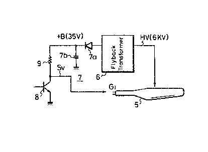
According to one aspect of the present invention
as represented in the embodiment of Fig. 3, a high-voltage
that is supplied to the flat type cathode ray tube 5 is
produced at a secondary of flyback txansformer 6, and a low
voltage supplied to ~he video output circui~ is produced
from anoth~r secondaxy of flyback transformer 6 and fed
through rec~ifier 7 to video output circuit 8 and the
current in video ou~put circuit 8 is inversely controlled
relative to ~he cathode cuxren~ in ~ube 5. Thus, both the
high-voltage and the DC low voltage for the video output
circuit 8 are supplied by a mutual output ~ransformer and
the present inventi.on strives to maintain the input power
constant to transformer 6. In other words t when -the cathode
current of the cathode ray tube 5 increases thereby tending
to lower the high-voltage, the current flowing t.hrouyh the
video circuit, that is, through transistor 8, is regulated
to become smaller, thereby suppressing high-voltage
fluctuations and keeping the high-voltage output ~o -tube 5
from decreasing. On the other hand~ when the cathode
current o-f tube 5 becomes smaller, thereby tending to raise
the high-voltage, the present invention operates so that the
current flowing through the video output circuit 8 will
increase to suppress high-voltage variations~
In Fig. 3, flyback transformer 6 will typically
produce at a secondary a high voltage HV that i5 in t,he
neighborhood of 6 kilovolts for this flat-type, black and
white, cathode ray tube 5. The high-voltage, of course~
would be much greater in the case of a color kelevision
tube. Additionall.y, a pulsed vol-tage is also produced by a
secondary of flyback transformer 6 and is s~lpplied to, and
xectified by, rectifier circuit 7 comprised of a serles
diode 7a and a capacitor 7b connected between the output of
diode 7a and relative ground potential, Rect.ifier 7 then
produces a reckified DC voltage (B-~) of approximately 35
volts~ The video ou~put amplifier is comprised of an NPN
transistor 8 that amplifies the video input signal applied
to the base ~hereof in the conventional fashion. In this
general representation, the emittar of transistor 8 is
connected to relative ground potential and the video output
signal Sv obtained at the collector is the positive polarity
video signal applied to first grid Gl of cathode ray tube 5~
J~ 3'.~ S02096
whereby cathode ~ay tube 5 is operated in the so-called G1
drive mode. In a commerical embodiment of the video output
circuit a resistor may be employed in the emitter circuit of
transistor 8. The video output transistor 8 is connected to
the B+ voltage produced by ~lyback transformer 6 through a
resistor 9, the value of which is spec.ifically chosen, as
taught by the present invention, to operate as cuxrent
regulator.
To bet~er unders~and this operation refer~nce is
had to Fig. 4, which shows the flyback transformer circuit 6
in more detail. In this circuit th~ high voltage for the
cathode ray tube 5 is produ~ed by a coilve~tional flyback
transformer lO as a pulsed signal and is rectified to a DC
signal by a rectifier circuit~ shcwn generally at 11. In
this embodiment the rectifier 11 is a simple half-wave .
rectifier formed using diodes in series wi~h smoothing or
filter capacitors connected in parallel therewith. Because
the ripple in this high-voltage .is at ~he horizontal
oscillator rate of 15,750 Hzl large value fi.lter capacitors
are not required. Flyback transformer lO is ene.rgized by a
voltaga from a DC power supply at a center tap 12 of a
primary winding that has connected at a lower end the
collector of -the hori~ontal deflection output transistor
circuit 13. This hori~ontal output deflectîon txansistor
circult 13 i5 conventio~al.
In the operation o~ the embodiment of FigO 3, the
high-voltage stabilizing circuit acts so that when the level
of the video signal Sv applied ~o the first grid G1 of the
cathode ray tub0 5 i5 relatively high causing a high cathode
current, which would tend to drive the high voltage
~7~
~ Jl~ S~0~6
supplied from flyback transformer 6 to cathode ray tube 5
lower, the current flowing through rectifier circuit 7 to
transistor ~ through resistor 9 is held small. Thus, it is
seen that if increases .in power of the video amplifier equal
decreases in power of the high vol-tage circuit, then the
overall input power will remain constant~ If such input
power remains constant the pulse height of the horizontal
output transistor will not vary and the voltage of the
high~voltage circuit is stabilized. In this way~ the pulse
height of the horizont~l output that results in the high
voltage at the secondary of flyback transformer 6 is
maintained, thereby suppressing any decrease in the high
voltage Hv. Conversely, when the video signal S~ fed to
first grid Gl of cathode ray ~ube 5 is of a relatively low
level, the cathode current of ~hP cathode ray tube 5 is
correspondingly lower the high-voltage supplied from the
fly~back transformer 6 to the cathode ray tube 5 would be
raised except that the currenk flow.ing f:rom the rectifier
circuit 7 to transistor 8 through resist.or 9 is increased
and the power consumed in the transistor 8 is increased,
thereby maintaining the pulse heigh~ of ~he pulse voltaye at
the secondary o the fly-back transformex 6 and suppressing
any increas~s in high voltage Hv in that case.
Note that the maximum power of the video output
ampliier is consumed under the condition when transistor 8
ls saturated and the minimum power consumption is zero that
ocsurs when transistor 8 is opened. The maximum power
typically consumed in a fla~-type cathode ray tube apparatus
is 1.2 watts.
In order to obtain such control of high-voltage
variations, the ohmic value of resistor 9 is selected to be
substantially lower than the value typically employed in
such a collector bias re~istor of a video output amplifier
80 The typical value for this collector bias resistor is
known to be axound 15 kohms. Because the value of this
resistor 9 is chosen to balance the circuit as shown in Fig.
3, its value is arrived empirically based on the impedances
of the other elements in the circuit. In a production model
of the SONY Watchman FD-20A, the resistance value of
resistor 9 following this invention would be selected to be
in a range of 1.2 Kohms to 1~8 Kohms.
Accordingly, based upon the present invention and
as evidenced by the embodiment discussed above~ regardless
o changes in the level of the video signal Sv that is fed
to the first grid Gl of cathode ray tube 5, the high-voltage
HV that is supplied to cathode ray tube 5 can be kept
constant. In this fashion, it is then possible by following
the teaching of the present invention to prevent the
position and size of the picture from varyirlg by maintaining
constant the high-voltage produced by the ~ly~ack
transformer.
Althou~h the above-described embodimerlt is
intended for use with the flat-type cathode ray ~ube, 5, ~he
present invention may also be applied to conventional
cathode ray tube configurations with the same advantageous
ef~cts. In such case J the bene~its are not qul-te so
conspicuous a5 shown in Fig. 1 above.
The above de~cription is provided for a single
preferred embodiment of ~che invention, however, i~ will be
apparent that many modif.ications and varlations could be
effected by one skilled in the art without departing from
the sp.irit or scope of the novel concepts of the invention
which should be determ.ined only by the appended claims.
..,
--10-'