Sélection de la langue

Search

Sommaire du brevet 1267349 

Énoncé de désistement de responsabilité concernant l'information provenant de tiers

Une partie des informations de ce site Web a été fournie par des sources externes. Le gouvernement du Canada n'assume aucune responsabilité concernant la précision, l'actualité ou la fiabilité des informations fournies par les sources externes. Les utilisateurs qui désirent employer cette information devraient consulter directement la source des informations. Le contenu fourni par les sources externes n'est pas assujetti aux exigences sur les langues officielles, la protection des renseignements personnels et l'accessibilité.

Disponibilité de l'Abrégé et des Revendications

L'apparition de différences dans le texte et l'image des Revendications et de l'Abrégé dépend du moment auquel le document est publié. Les textes des Revendications et de l'Abrégé sont affichés :

  • lorsque la demande peut être examinée par le public;
  • lorsque le brevet est émis (délivrance).
(12) Brevet: (11) CA 1267349
(21) Numéro de la demande: 1267349
(54) Titre français: METHODE DE FABRICATION DE DISPOSITIFS A SEMICONDUCTEUR PLANAR A TRANCHEE
(54) Titre anglais: METHOD OF MAKING A PLANAR TRENCH SEMICONDUCTOR STRUCTURE
Statut: Périmé et au-delà du délai pour l’annulation
Données bibliographiques
(51) Classification internationale des brevets (CIB):
  • H01L 21/312 (2006.01)
  • H01L 21/311 (2006.01)
  • H01L 21/76 (2006.01)
  • H01L 21/762 (2006.01)
(72) Inventeurs :
  • DOUGHERTY, JAMES J. (Etats-Unis d'Amérique)
(73) Titulaires :
  • INTERNATIONAL BUSINESS MACHINES CORPORATION
(71) Demandeurs :
  • INTERNATIONAL BUSINESS MACHINES CORPORATION (Etats-Unis d'Amérique)
(74) Agent: RAYMOND H. SAUNDERSSAUNDERS, RAYMOND H.
(74) Co-agent:
(45) Délivré: 1990-04-03
(22) Date de dépôt: 1986-05-05
Licence disponible: S.O.
Cédé au domaine public: S.O.
(25) Langue des documents déposés: Anglais

Traité de coopération en matière de brevets (PCT): Non

(30) Données de priorité de la demande:
Numéro de la demande Pays / territoire Date
793,400 (Etats-Unis d'Amérique) 1985-10-31

Abrégés

Abrégé anglais


Abstract
METHOD OF MAKING A PLANAR TRENCH SEMICONDUCTOR STRUCTURE
A method is provided for making a planar surface on a
semiconductor substrate having a trench or groove formed
therein and filled with a material such as an organic
material which may be used to electrically isolate one
region of the substrate from an adjacent region of the
substrate. The method includes the steps of forming a
trench or groove in a semiconductor substrate through a
surface thereof, depositing an organic or other filling
material on the surface of the substrate and into the
trench, forming a block of material over the trench on the
filling material so as to extend a given distance over the
surface of the substrate, etching the filling material
with a given etchant so as to remove he filling material
disposed over the surface of the substrate until only a
segment of the filling material remains over the trench
and above the surface of the substrate, forming a layer of
material over the surface of the semiconductor substrate
so as to cover the segment of the filling material, with
the layer of material and the filling material having
similar etch rates, and etching simultaneously the layer
of material and the segment of the filling material until
all of the layer of material is removed from the surface
of the semiconductor substrate. In a preferred embodiment
of this invention, the filling material is polyimide, the
block of material and the layer of material are
photoresists and each of the etching steps is carried out
with a directional dry etching process using 100% oxygen
gas as the etchant.
BU9-84-024

Revendications

Note : Les revendications sont présentées dans la langue officielle dans laquelle elles ont été soumises.


- 8 -
The embodiments of the invention in which an exclusive
property or privilege is claimed are defined as follows:
1. A process for making a semiconductor
structure which comprises the steps of
forming a groove in a solid body through a
surface thereof,
depositing a first material into said
groove and on said surface,
forming a block of material over said
groove so as to extend a given distance over
said surface,
etching said first material while leaving a
segment of said first material under said block,
forming a layer of second material over the
surface of said body so as to cover the segment
of said first material, said layer of second
material and said first material having similar
etch rates, and
etching simultaneously said layer of second
material and said first material until the
surface of said body is exposed.
2. A process as set forth in Claim 1 wherein
said first material is a polyimide.
BU9-84-024

- 9 -
3. A process as set forth in Claim 1 wherein
each of said etching steps is a dry etching
process.
4. A process as set forth in Claim 1 wherein
said block is made of a photoresist material.
5. A process as set forth in Claim 1 wherein
said layer of second material is a photoresist
material.
BU9-84-024

- 10 -
6. A process for making a semiconductor
structure which comprises the steps of
forming a trench in a semiconductor body
through a surface thereof,
depositing an organic material into said
trench and on said surface,
forming a block of material over said
trench so as to extend a given distance over
said surface,
etching said organic material with a given
etchant so as to remove said organic material
deposited over said surface while leaving a
segment of said organic material over said
trench,
forming a layer of material over the
surface of said semiconductor body so as to
cover the remaining portion of said organic
material over said trench, said layer of
material and said organic material having
similar etch rates, and
etching said layer of material and said
organic material until all of said layer of
material is removed.
BU9-84-024

- 11 -
7. A process as set forth in Claim 6 wherein
said organic material is a polyimide.
8. A process as set forth in Claim 6 wherein
each of said etching steps is a directional dry
etching process.
9. A process as set forth in Claim 6 wherein
each of said etching steps includes the use of a
100% oxygen gas etchant.
10. A process as set forth in Claim 6 wherein
said block is made of a photoresist material.
11. A process as set forth in Claim 6 wherein
said layer of material is a photoresist
material.
BU9-84-024

- 12 -
12. A process for making a semiconductor
structure which comprises the steps of
forming a trench in a semiconductor body
through a surface thereof,
flowing an organic material having a high
molecular weight into said trench and on said
surface,
curing said organic material,
forming a block of photoresist over said
trench so as to extend a given distance over
said surface,
etching said organic material so as to
remove said organic material on said surface
while leaving a segment of said organic material
over said trench,
forming a layer of photoresist over the
surface of said semiconductor body so as to
cover the segment of said organic material over
said trench, said layer of material and said
organic material having similar etch rates, and
etching simultaneously said layer of
material and said organic material until all of
said layer of material is removed.
BU9-84-024

- 13 -
13. A process as set forth in Claim 12 wherein
said organic material is a polyimide.
14. A process as set forth in Claim 12 wherein
each of said etching steps is a directional dry
etching process.
15. A process as set forth in Claim 12 wherein
each of said etching steps includes the use of a
100% oxygen gas etchant.
BU9-84-024

- 14 -
16. A process for making a semiconductor
structure comprising the steps of
growing an epitaxial layer on a semicon-
ductor substrate,
forming an electrically isolating layer at
the interface between said epitaxial layer and
said substrate,
forming a trench through the surface of
said epitaxial layer and said isolating layer
into said semiconductor substrate,
flowing an organic material having a high
molecular weight into said trench and on the
surface of said epitaxial layer,
curing said organic material,
forming a block of material over said
trench so as to extend a given distance over the
surface of said epitaxial layer, said organic
material and said block having similar etch
rates for a given etchant,
etching simultaneously said organic material
and said block with said given etchant so as to
remove said block and said cured organic material
on the surface of said epitaxial layer until
only a segment of said cured organic material
remains over said trench and on the surface of
said epitaxial layer adjacent said trench,
BU9-84-024

- 15 -
(Claim 16 Continued)
flowing a layer of material having a low
molecular weight over the surface of said
epitaxial layer so as to cover the segment of
said cured organic material, said layer of
material and said organic material having
similar etch rates for said given etchant, and
etching said layer of material and said
organic material until the surface of said
epitaxial layer is exposed.
BU9-84-024

- 16 -
17. A process as set forth in Claim 16 wherein
said organic material is polyimide having a
molecular weight greater than 8000 grams/gram-
mole.
18. A process as set forth in Claim 16 wherein
said block and said layer of material are made
of photoresist.
19. A process as set forth in Claim 16 wherein
said forming and etching steps include reactive
ion etching.
BU9-84-024

- 17 -
20. A process for making a semiconductor
structure which comprises the steps of
forming a trench in a semiconductor sub-
strate through a surface thereof,
flowing a polyimide having a molecular
weight greater than about 8000 grams/gram-mole
into said trench and on the surface of said
substrate,
curing said polyimide,
forming a block of photoresist on said
cured polyimide and over said trench so as to
extend a given distance over said surface from
said trench, said cured polyimide and said block
of photoresist having similar etch rates for a
given etchant,
etching simultaneously said cured polyimide
and said block until said surface is exposed 50
as to form a segment of said cured polyimide
above the surface of said substrate at said
trench,
flowing a layer of photoresist having a low
molecular weight compared to that of said
polyimide over the surface of said substrate so
as to cover said polyimide segment, said layer
of photoresist and said polyimide having similar
etch rates, and
etching said layer of photoresist and said
polyimide until the surface of said substrate is
exposed.
BU9-84-024

- 18 -
21. A process as set forth in Claim 20 wherein
said forming and etching steps include a
directional reactive ion etching process.
22. A process as set forth in Claim 20 wherein
each of said etching steps includes the use of a
100% oxygen gas etchant.
BU9-84-024

Description

Note : Les descriptions sont présentées dans la langue officielle dans laquelle elles ont été soumises.


~;~67~ 3
--1--
Description
METHOD OF MAKING A PLANAR TRENCH SEMICONDUCTOR STRUCTURE
Technical Field
. _ _
This invention relates to a method of making
integrated semiconductor circuit structures and more
particularly to a method of making planar semiconductor
structures having filled grooves or trenches.
Background Art
Grooves or trenches filled with insulating material,
such as silicon dioxide or polyimide, for isolating
devices, e.g., transistors, from one another, in integrated
semiconductor circuits have been known to provide signifi-
cant device or transistor density improvements over other
known isolation techniques such as those employing P-N
junctions.
In IBM*Technical Disclosure Bulletins, Vol. 17, No.
10, Marchl 1975, pp. 2893-2894, there`is disclosed a
V-groove trench filled with polyimide, Vol. 24, No. llA,
April, 1982, pp. 5458-5459, there is disclosed a transistor
butted against the sidewall of a trench filled with
insulating material, Vol. 23, No. 11, April, 1981, pp.
4917-4919, there is disclosed a trench filled with silicon
dioxide and sil.icon nitride with portions of the silicon
nitride being removed by a reactive ion etching ~RIE3
technique and Vol. 25, No. llB, April, 1983, pp. 6129-6130,
there is disclosed a method for filling a trench with
silicon dioxide and planarizing the silicon dioxide with
respect to the surface of the substrate in which the
trench was formed.
* Registered trade mark
~d
BU9-84-024

3 ;~ 4~
U.S. Patent No. 4,396,460, filed May 21, 1982, and
issued August 2, 1983, discloses a method for obtaining
surface flatness at a groove in a semiconductor substrate
by employing chemical etching and a double ~ayer film
which is made of two different substances.
In commonly assigned U.S. Patent No. 4,519,128, filed
on October 5, 1983, by D. G. Chesebro and F. J. Soychak
and issued on May 28, 1985~ there is disclosed a trench
formed in a semiconductor substrate having thin layers of
silicon dioxide and silicon nitride formed on the
sidewalls and bottom of the trench, with the remainder of
the trench filled with polyimide. Any excess polyimide is
removed after being thermally cured by known etch back
techniques.
It has been found that when the filling material in a
trench is etched back an undesired step is formed between
the surface of the substrate and the top of the filling
material due to either over etching or under etching the
filling material and due to the contour of the filling
material at the trench. Such a step causes discontinuities
in conductive lines or wiring subsequently formed over the
substrate which reduces the reliability of these integrated
circuits.
Disclosure of the Invention
It is an object of this invention to provide an
- improved simple planarization method for semiconductor
substrates having narrow grooves or trenches, e.g., less
than 2 microns wide, formed therein and filled with,
particularly organic material, such as polyimide.
BU9-84-024

126t7~ 3
In accordance with the teachings of this invention a
method is provided for making a planar surface on a
semiconductor substrate having a groove or tr~nch formed
therein and filled with a material such as an organic
material which may be used to electricall~ isolate one
region of the substrate from an adjacent region. The
method includes the steps of forming a groove or trench in
a semiconductor substrate through a surface thereof,
depositing a filling material, such as an organic
material, within the trench and on the surface of the
substrate, forming a block of material over the trench on
the organic material so as to extend a given distance over
the surface of the substrate, etching the organic material
and the block with a given etchant so as to remove the
lS block and the organic material disposed over the surface
of the substrate, forming a layer of material over the
surface of the semiconductor substrate so as to cover the
remaining portion of the organic material, with the layer
of material and the organic material having similar etch
2~ rates with a given etchant and etching the layer of
material and the organic material until all of the layer
of material is removed.
In a preferred embodiment of this invention, the
organic material is polyimide, each of the etching steps
2~ is carried out with a dry etching process, the etchant
being 100% ox~gen gas, the block of material is
photoresist and the layer of material is also photoresist.
The foregoing and other objects, features and advan-
tages of the invention will be apparent from the ollowing
and more particular description of the preferred embodi-
ments of the invention, as illustrated in the accompanying
drawings.
BU9-84-0~4

~L21~;34~
--4--
Brief De~scription of the Drawings
Figs~ l, 2, 3 and 4 are sectional views of a structure
having a trench formed in a semiconductor substrate taken
at succeeding stages during the fabrication of the struc-
ture made in accordance with the teachings of the present
invention.
Best_Mode for Carr~in~ _ut the Invention
Referring to the drawings in more detail there is
.illustrated in sectional view in Fig. 1 a structure which
includes a semiconductor substrate lOf preferably made of
silicon, having a P type conductivity and an epitaxial
layer 12 having a surface 14 and of N type conductivity
grown on the substrate 10 by known techniques with an N+
subcollector diffusion region 16 formed at the junction of
the substrate 10 and the epitaxial layer 12.
By using an appropriately patterned photoresist mask
with, for example, nitrogen triflouride, not shown, and
known reactive ion etching (RIE~ techniques, a trench 18,
e.g., 2 microns wide, is formed through the epitaxial
layer 12 and the N~ subcollector region 16 into the
substrate 10 to a depth of approximately 5.0 microns below
the surface 14 of the epitaxial layer 12 to form isolated
sections 12A and 12B in the epitaxial layer 12. The
trench 18 is then filled with polyimide, preferably by
depositing a first layer of about 3~5 microns of DuPont*
2560 polyimide on the surface of the epitaxial layer 12
and allowing the polyimide to flow into the trench 18
during a spinning operation, curing the first polyimide
layer at 80C for 13 minutes and then depositing a second
layer of about 3.5 microns of DuPont 2560 polyimide over
the first polyimide layer and curing the second polyimide
layer at 400C for 25 minutes. Using reactive ion etching
* Registered trade mark
BU9-84-024

-` 12~i~349
--5--
(RIE) techniques with oxygen as the etchant, the cured
polyimide, not shown, on the surface 14 of the epitaxial
layer 12, is removed with polyimide 20 remaining in the
trench 18 to a level somewhat below the surface 14 of the
epitaxial layer 12. The trench 18 is then completely
filled with DuPont 2560 polyimide until a layer 22 of
cured polyimide, about 1.3 microns thick, is formed on the
surface 14 of the epitaxial layer 12, as indicated in Fig.
l of the drawings. After curing the polyimide layer 22,
which may have been performed at 400C for 25 minutes, a
depression or groove 24 is known to form in the cured
polyimide layer 22 over the trench 18. It has also been
noted that after curing the polyimide, there are
variations in the thickness of the polyimide layer 22 over
the surface 14 of the epitaxial layer 12. By setting a
target thickness of 1.3 microns for the cured polyimide
layer 20, it has been found that the lowest point in the
depression or groove 24 is located above the surface 14 of
the epitaxial layer 12.
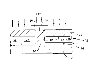
A layer of photoresist, about 2.4 microns thick, is
now deposited on the polyimide layer 22 and, with an
appropriately patterned mask, a photoresist segment or
block 26 is formed over the trench 18 with extensions of
the block 26 overlapping the surface 14 of the epitaxial
layer 12 adjacent to the trench 18. The photoresist block
26 is made preferably with substantially vertical
sidewalls. By again using reactive ion etching (RIE~
techniques with oxygen as the etchant, the polyimide layer
22 is removed from the surface 14 of the epitaxial layer
12 except for the polyimide in the vicinity of the trench
18 under the photoresist block 26 where a polyimide
segment 28, about 1.3 microns thick, is formed over the
trench 18 and on the surface 14 of the epitaxial layer 12
adjacent to the trench 18, as indicated in Fig. 2 of the
drawings.
BU9-84-024

~l~6~3~63
--6--
The polyimide segment 28 is then covered with a layer
of photoresist 30, as shown in Fig. 3, which may be of the
same type as photoresist block 26 9 having a thickness of
about 1.4 microns and having an etch rate similar to that
of the polyimide block 28. The layer of photoresist 30
and the polyimide segment 28 are now removed by reactive
ion etching (RIE) techniques with oxygen as the etchant to
provide a planarized surface wherein it has been found
that the upper surface 32 of the polyimide 20, as shown in
Fig. 4, in the trench 18 is always less than 0.5 microns
above the surface 14 of the epitaxial layer 12 or less
than 0.3 microns below the surface 14 of the epitaxial
layer 12. Thus, when a conductive line or electrical
wiring is extended over the trench 18 between isolated
sections 12A and 12B of the epitaxial layer 12, there is
little or no likelihood that discontinuities will occur in
the line or wire at the surface of the trench 18.
It should be understood that preferred polyimides for
filling the groove or trench 18 are those that have a
molecular weight greater than approximately 8000 grams/-
gram-mole. This type of polyimide is desired because the
mechanical properties of lower molecular weight polyimides
tend to be brittle and result in material defects such as
delamination and in-situ fracturing after a trench filling
operation. Although these higher molecular weight
polyimides tend to produce non-planar surfaces due to the
low relative solids content and viscous nature, by the use
of the teachings of this invention a process is provided
wherein very planar surfaces are repeatedly produced even
with the use of polyimides having a molecular weight
greater than approximately 8000.
In the preferred embodiment of this invention,
polyimide is used as a trench filling material, however,
this invention may be practiced by using materials other
BU9-84-024

~l2~ 34~3 ~D
--7--
than polyimide, e. g., glass, given that appropriate
reactive ion etching conditions and etchants are used to
provide similar etch rates between the photoresist and the
glass when reactively ion etching as indicated in Fig. 3
of the drawings.
It should also be noted that the proce~s of this
invention may be used advantageously to isolate one
sPmiconductor region from another semiconductor region
when making either bipolar transistors in regions 12A and
12B or when making field effect transistors.
Accordingly, it can be seen that this invention
provides a very simple process for producing a highly
planarized semiconductor structure when one or more
trenches are formed in the structure resulting in improved
reliability and higher yields for highly dense semi-
conductor circuits.
While the invention has been particularly shown and
described with reference to preferred embodiments thereof,
it will be understood by those skilled in the art that
various changes in form and details may be made therein
without departing from the spirit and scope of the inven-
tion.
~;~
.~
BU9-84-024

Dessin représentatif
Une figure unique qui représente un dessin illustrant l'invention.
États administratifs

2024-08-01 : Dans le cadre de la transition vers les Brevets de nouvelle génération (BNG), la base de données sur les brevets canadiens (BDBC) contient désormais un Historique d'événement plus détaillé, qui reproduit le Journal des événements de notre nouvelle solution interne.

Veuillez noter que les événements débutant par « Inactive : » se réfèrent à des événements qui ne sont plus utilisés dans notre nouvelle solution interne.

Pour une meilleure compréhension de l'état de la demande ou brevet qui figure sur cette page, la rubrique Mise en garde , et les descriptions de Brevet , Historique d'événement , Taxes périodiques et Historique des paiements devraient être consultées.

Historique d'événement

Description Date
Inactive : CIB de MCD 2006-03-11
Le délai pour l'annulation est expiré 2000-04-03
Lettre envoyée 1999-04-06
Accordé par délivrance 1990-04-03

Historique d'abandonnement

Il n'y a pas d'historique d'abandonnement

Historique des taxes

Type de taxes Anniversaire Échéance Date payée
TM (catégorie 1, 8e anniv.) - générale 1998-04-03 1997-11-12
Titulaires au dossier

Les titulaires actuels et antérieures au dossier sont affichés en ordre alphabétique.

Titulaires actuels au dossier
INTERNATIONAL BUSINESS MACHINES CORPORATION
Titulaires antérieures au dossier
JAMES J. DOUGHERTY
Les propriétaires antérieurs qui ne figurent pas dans la liste des « Propriétaires au dossier » apparaîtront dans d'autres documents au dossier.
Documents

Pour visionner les fichiers sélectionnés, entrer le code reCAPTCHA :


Pour visualiser une image, cliquer sur un lien dans la colonne description du document. Pour télécharger l'image (les images), cliquer l'une ou plusieurs cases à cocher dans la première colonne et ensuite cliquer sur le bouton "Télécharger sélection en format PDF (archive Zip)" ou le bouton "Télécharger sélection (en un fichier PDF fusionné)".

Liste des documents de brevet publiés et non publiés sur la BDBC .

Si vous avez des difficultés à accéder au contenu, veuillez communiquer avec le Centre de services à la clientèle au 1-866-997-1936, ou envoyer un courriel au Centre de service à la clientèle de l'OPIC.


Description du
Document 
Date
(aaaa-mm-jj) 
Nombre de pages   Taille de l'image (Ko) 
Page couverture 1993-10-14 1 16
Revendications 1993-10-14 11 194
Abrégé 1993-10-14 1 44
Dessins 1993-10-14 1 21
Description 1993-10-14 7 274
Dessin représentatif 2000-07-10 1 6
Avis concernant la taxe de maintien 1999-05-04 1 179
Taxes 1996-11-29 1 43
Taxes 1995-12-11 1 45
Taxes 1994-11-30 1 50
Taxes 1993-12-17 1 38
Taxes 1992-01-17 1 30
Taxes 1993-01-05 1 14