Note : Les descriptions sont présentées dans la langue officielle dans laquelle elles ont été soumises.
~.Z6~
The present invention relates to a me~hod
of manufacturing an electric resistance element.
Electric resistance elements have hitherto
been generally manufac-tured by coating a resistance
paste material prepared from carbon particles and organic
synthetic resin on the surface of an insulator by a
method such as screen printing to ~orm a resistance
film.
A conventional method of manufac-turing an
electric resistance element comprises kneading carbon
particles and a solution of thermosetting resin to prepare
a paste material; screen-printing the paste material
on the sur:Eace of a substrate (particularly an insula-tor
such as a laminated plate of phenol resin or epoxy resin,
an alumina ceramic plate or a metallic core subs-trate)
in the form of a pattern; removing solvent by applica-tion
of heat and fur-ther heating the substrate at a temperature
of, e.g. 100 to 150C, to cure the resin and thereby
Eorm a resistance film; and mounting an electrode on
part of the resistance film by means of a conductive
paint such as silver paste. The thermosetting resin
is prepared using phenol resin, epoxy resin, mel~mine
resin, urea-formaldehyde resin, alkyd resin or acrylic
resin, or a mixture thereof~
However, electric resistance elements manu~actured
by this conventional me-thod have significant disadvantages
and they are extremely varied in resistance and inferior
in stability against the environment. The most likely
cause for such disadvantages is that the carbon particles
are non-uni~ormly arranged in the resin while -the resin
is non-uniformly adhered to the surfaces of the carbon
particles, whereby the interfaces between the carbon
par-ticles vary, leading to unstable contact resistance.
This is based on the principle that the resistance of
an electric resistance element is determined not by
volume speciEic resistance of carbon particles, but
by contact resistance thereof.
~2~
An o~ject of the present invention is to provide
a method of manufacturing an electric resistance element
whiGh avoids the disadvantages as h0reinabo~e described.
In order to overoome the aforementioned
di~advanta~e~, it i8 necessary to make uniform and
~tabilize the surfaces of carhon particles, to uniformly
disper~e the ~ame ln resin.
Accordlngly, the present invention provides a
method of manufacturing an electric resistance element,
compri~ing the ~tep~ of: ~a) thermally treating carhon
partiGles at a temperature of at lea~t ~00C, (h) mixing
the carbon partiçles with a solution of an amino resin in
a firs~ solvent and heatin~ the mixttlre to cau~e at least
partial reaction between the çarbon particles and the
amino resin and polymerizing the amino resln by heating,
(c) mixing a ~olution of an epoxy resin in a second
solvent with the mlxture to prepare a paste material, and
(d) coating the pa~te material on the surface of a
sub~trate and thermally curing the paste material, thereby
to form a resistanGe film nn the surfaçe of said
substrate.
The present invention is characterized in that
the carbon particles are thermally treated at a
temperature of at least 300DC and that two types of refiin
materials, i.e~ amino resin and epo~y resin are employed.
The carbon particles may comprise acetylene
: black, furnase black, channel black, thermal hlack or the
like, and the ~rain size thereof is preferably from 0.001
to 1.0~ ~m.
The amlno resin may be a general amino resin,
preferably in the form of a polymer of a reaGtant
(methylol urea or methylol melamine) of urea or melamine
and formaldehyde, particularly a polymer of methylol urea
or methylol melamine reacted on alcohol ~particularly
3~ methanol or butanol). The methylol urea or methylol
melamine may be employed in unreaçted form, i.e. in the
form of a
mixture of melamine or urea and formaldehyde. The molecular
ratio of melamine or urea to formaldehycle is preferably
from 1.0:1.0 to 1.0:0.3.
The epoxy resin is preferably of the bisphenol
A type, while the novolac phenol -type i9 also employable.
The substrate is generally an organic material
such as paper, phenol resin, epoxy resin or polyimide
or a laminated plate thereof, alumina ceramic, various
ceramics, a glass pla-te or a metallic core substrate,
or one previously formed with a resistance terminal
part by a metal such as ~g, Au or Ag-Pd or a conductive
paint with a conductor of such metal.
The method according to the present invention
will now be described in detail.
(a) Carbon particles are thermally treated
at a temperature of at least 300~C. The -temperature
!~ :Eor the heat treatment is preferably 400 to 500C. The
heat treatment is preferably performed for a period
exceeding that in which gas generation occurs. In this
case, the heat treatment is preferably performed under
decompression through, e.g., a water aspirator. The
carbon particles generally adsorb gas, moisture and
the like generated in the manufacturing process, and
such adsorbed materials are removed by the said heat
treatment. Thus, the carbon particles are activated
and the surfaces thereof are rendered uniEorm. Cooling
after the heat -treatment is preferably performed in
a closed system so that the carbon particles are not
in contact with fresh air.
~b) The carbon particles are mixed with a
solution of amino resin and heated to a-t least partially
cause reaction of the carbon particles with the amino
resin and polymerization of the amino resin. The amino
resin is preferably added by aspiration under decompression.
The weight ratio of the carbon particles to the amino
resin is generally from 1:1 to 1:5. The amino resin
is previously dissoived in a solvent so as to be employed
~2~
in the form of a solution. A solvent can be employed
which is ca~able of dissolviny the amino resin. Preferred
solvents are, e.g., n-butanol, MEK, diacetone alcohol
or cellosolve. The concentration of this solution is
generally 40 to 60~, al-though this can be varied with
the type of amino resin and solvent. A carbon-resin
partially polymerized polymer (hereinafter referred
to as "CB mixture") is formed by heating, whereby the
surfaces of the carbon particles are rendered uniform
and stabilized. The reaction by heating is preferably
performed such that the degree oE polymerization oE
the amino resin reaches 1/3 to 1/2 of the final degree
of polymerization thereof. The heating temperature
and time for the reaction are, or example, at least
100C and several tens oE minutes, although the condi-tions
can be varied with the types and volume oE the carbon
particles and the amino resin. The reaction is terminated
by discontinuing the heating and lowering the temperature
to, e.g., room temperature. Although the reaction is
preferably performed after evaporation oE the solvent
for the amino resin, such evaporation may be completed
during the reaction. The solvent is preEerably evaporated
under a decompressed sta-te in a vacuum, for example.
; tc) A solutlon of epoxy resin is mixed with
the CB mixture to prepare a paste material. The weight
ratio of the epoxy resin to the amino resin is preferably
from 1:1.2 to l:l. As the solvent for the solution
of epoxy res:in, any solvent can be employed which is
capable of dissolving the epoxy resin, preferably e.g.,
butyl cellosolve. The concentration of the epoxy resin
solution is generally Erom 40 to 60%, although this
can be varied depending on the type of epoxy resin and
solvent as employed. A uniEorm paste material can be
prepared by sufficient kneading and dispersion.
~d) The pas-te material is coated on the surface
of a substrate and subjected to curing to form a resistance
film on the surface of the substrate. In advance of
~26~
the coating process, solvent is further added to the
pas-te material to appropriately adjust its viscosity
for coating. The viscosity of the paste material in
the coating process is generally from 40,000 to 80,000
cps. The paste material is coated by screen printing,
preferably through a screen of from 200 to 325 mesh.
Af-ter the screen prin-ting, levelling is preferably performed
by leaving the substra-te for five to 10 minutes at
room tempera-ture. The paste material is generally cured
!, 10 by hea-ting the same a-t a temperature of from 150 to
200~C for 90 to 1~0 minutes, although the heating temperature
and time can be varied with the composition of the past
material employed. Although it is preEerable -to evaporate
-the solvent con-tained in the pas-te material in advance
of the curing process, such evaporation may also be
performed af-ter the paste material is cured. The resistance
film is preferably formed after a -terminal electrode
is provided on the substrate, while the -terminal electrode
may also be provided af-ter formation of -the resis-tance
film. The final thickness of the resistance film thus
formed is preferably from 10 to 20 microns in general.
If necessary, a protective coating is formed on the
resistance film.
In the resistance film formed by the method
according -to the present inven-tion, carbon particles
and epoxy resin are regularly arranged through a~ino
resin. Thus, the carbon particles are uni:Eormly dispersed
and arranged in the electric resistance film.
Typical advantages of the present inven-tion
are as follows: (1) small variation in resistance
(good reproducibility); (2) high stability agains-t
the environment; (3) good current load charac-teris-tic:
the current load characteristic of the resistance element
according to the present invention is about 45 mW/mm2
while that of the conventional element has been about
15 mW~mm ; and (4) low current noise.
Such advantages are obtained since the carbon
~267~
particles are rendered uniform in the surface skate
and uniEorml.y arranged wi-th removal of the adsorbed
materials.
The elec-tric resistance element according
to the present invention is suitable for a slidabl.e
or fixed resistor, to be applied to an in-tegrated circuit
or the like. When the resistance element is applied
to a fixed resistor, the same is preferably protec-ted
by an appropriate protective coat such as an insulating
moisture-proof coat.
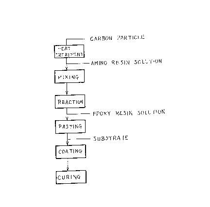
In the accompanying drawings:
Fig. 1 is a diagram illustrating schematically
an embodiment of the method according to -the present
invention.
The :Eollowing Examples illustrate the present
invention.
Example 1
100 g of acetylene black particles of 0.01
to 0.5 ~m in mean grain size were thermally treated
in a procelain vessel with a stock cock at 380C under
normal pressure for 47 minutes, and then cooled to
room temperature. A solution of 150 g of methylated
methylol melamine and 300 ml of a solvent comprising
a butanol/cellosolve equivalent-weight mixture was added
to the carbon particles, which were then heated at 80C
for two hours to remove the solven-t, and again heated
at 120C for 35 minutes to cause reaction. Then the
mixture was ~uenched to room temperature, and a solution
of 150 g of bisphenol A type epoxy resin ~epoxy equivalent
(EV) - 500) and 150 ml of butyl cellosolve was added
and sufficiently kneaded to prepare a paste material.
The paste material contained about 70 percent by weight
of solid components. Butyl cellosolve was further added
to adjust the con-tent of the solid components to 60
to 65 percent by weight thereby to obtain viscosity
of 68,000 cps. The paste material was coated on the
surface of a single-face copper-plated glass epoxy substra-te
~.2~
through a screen of 250 mesh, to form a film of 17.5
microns in thickness. Then the coated substrate was
heated at 170C for 90 minu-tes to cure the film, thereby
to form a resistance element. The final thickness of
the film was 15 microns. Design sheet resistivity of
the resistance element was 3.75 kQ/~ , while measured
sheet resistivity was 3.5 k~/o .
Example 2
78 g of thermal black particles of 0.5 to
l.0 ~m in mean grain size were thermally treated in
a procelain vessel with a stock cock at 430C under
a pressure lower by 55 mmHg than normal pressure for
40 minutes, and then cooled to room temperature.
solu-tion of 150 g of butylated methylol melamine and
150 ml of a solvent comprising a butanol/MEK e~uivalent
volume mixture was added to -the carbon particles, which
were then heated at 85C for 1.5 hours to remove the
solvent, and further heated at 100C for 35 minutes
to cause reaction. Then the mixture was quenched to
room temperature, and a solution of 150 g of bisphenol
A type epoxy resin (EV = 500) and 150 ml of butyl cellosolve
was added and sufficiently kneaded to prepare a paste
material. The paste material contained about 71 percent
by weight of solid components. Butyl cellosolve was
25 further added to adjus-t the viscosity to 70,000 cps,
and the paste material was coated on the surface of
a single-face copper-plated glass epoxy substrate through
a screen of 250 mesh, to form a film of 18.0 microns
in thickness. Then the coated substrate was heated
30 at 170C for 90 minu-tes to cure the film, thereby to
form a resistance element. The final thickness of the
film was 15 microns. Design sheet resistivity of the
resistance elemen~ was 5.0 kQt~ , while measured sheet
resistivity was 4.75 k~/o -
Example 3
57 g of channel black particles of 0.001 to
0.03 ~m in mean grain s:ize were thermal]y treated in
~2~
a porcelain vessel wi-th a stock cock at 415C under
normal pressure for 65 minu-tes, and cooled to room tempera-
ture. A solution of 150 g of butylated methylol urea
and 150 ml of MEK was added to the carbon particles,
which were then heated at 80C for one hour to remove
the solven-t, and further heated at 100C for 35 minutes
to cause reaction. Then the mixture was quenched to
room temperature, and a solution of 150 g of bisphenol
A type epoxy resin (EV = 750) and 100 ml of butyl cellosolve
was added and sufficiently kneaded to prepare a paste
material. The paste material contained about 78 percent
by weight of solid components. Butyl cellosolve was
further added to adjust the viscosity to 70,000 cps,
and the paste material was coated on a single-Eace copper-
plated glass epoxy substrate through a screen oE 250mesh, to form a :Eilm oE 16.0 microns in thickness. Then
the coating substrate was heated at 180C for 120 minutes
- to cure the film, thereby to form a resistance element.
The final thickness of the film was 15 microns. Design
sheet resistivity of the resistance element was 7.5
kQ/~ , while measured sheet resistivity was 6.3 kQ/~ .
Example 4
35 g of furnace black particles of 0.05 -to
0.1 ~Im in mean grain size were thermally -treated in
a porcelain vessel with a stock cock at 450C under
a pressure lower by 30 mmHg than normal pressure for
70 minutes, and then cooled to room temperature. A
solution of 150 g of methyla-ted methylol urea and 150
ml of MEK was added to the carbon particles, which were
then heated at 85C for two hours to remove the solvent,
and further heated at 130C for 25 minutes to cause
reaction of urea-formaldehyde resin. Then the mixture
was quenched to room tempera-ture, and a solution of
180 g of bisphenol A type epo~y resin (EV = 750) and
180 ml of butyl cellosolve was added and sufficien-tly
kneaded to prepare a paste material. The paste material
contained abou-t 67 percent by weight of so]id components.
9~B~
sutyl cellosolve was fur-ther added to adjust the viscosity
-to 68,000 cps, and the paste material was coated on
the surface of a single-face copper-plated glass epoxy
substrate through a screen of 250 mesh, -to form a film
of 16.0 microns in thickness. Then the coated substrate
was heated at 180C for 120 minutes to cure the ilm,
thereby to form a resistance element. rrhe final thickness
of the film was 15 microns. Design sheet resistivity
of the resistance element was 25 kQ/~ , while measured
sheet resistivity was 26.5 kQ/~ .
Reference Example 1
A solution of 300 g of epoxy resin (EV = 500)
and 350 ml of butyl cellosolve was added to 150 g of
ace-tylene black pa.rticles of 0.01 to 0.5 ~m in mean
gra:in size and sufficiently kneaded to prepare a paste
material. The paste material contained 57.0 percent
by weight o:E solid components. 6.0 phr o:E an amine
curing a~ent (ethylene diamine) was added to the paste
material to attain a viscosity of 62,000 cps, and coated
on a single-face copper-plated glass epoxy substrate
through a screen of 250 mesh, to form a film of 18.0
. microns in thickness. Then the coated substrate was
: heated at 180C :Eor 90 minutes to cure the film, thereby
to form a resistance element. The final thickness of
the film was 15 microns. Design sheet resistivity of
the resistance.element was 4.3 kQ/~ , while measured
sheet resistivity was 4.0 kQ/~ .
Reference Example 2
A solution of 230 g of epoxy resin (EV = 350)
and 220 ml of butyl cellosolve was added to 150 g of
acetylene black particles of 0.5 to 1.0 ~m in mean grain
size and sufficiently kneaded to prepare a paste material.
The paste material contained 63.5 percent by weight
of solid components. 8 phr o:E a curing agent comprising
diethylenetri.ami.ne was aclded to the paste material to
attain a viscosity Or 63,000 cps and coated on a single-
face copper-plated glass epoxy substrate -through a screen
~2~79~
of 250 mesh, to Eorm a film of 15.7 microns in thickness.
Then the coated substrate was heated at 180C for 90
minutes to harden the film, thereby to form a resistance
element. The final film thickness was 15 micxons. Design
sheet resistivity of the resistance element was 1.5
k~ , whi:Le measured sheet resistivity was 1.75 k~/~ .
Experiments
The resistance elements manufactured by Examples 1
to 4 and Reference E~amples 1 and 2 were subjected to
evaluation of electric characteristics, resistance tempera-
ture characteristics and reliability. The results are
shown in the following Table 1, which also shows the
results of levelling.
~IL;;~6~
rl _ c--- In O O n o~ ~3
~ ~Q '~1 + ~i~ ~ + ~ r~ +
., a) ,~ ~_ _ . _ . ,
~,a o O r~ L~o,, O o ,~
,I Q ,~ (`I co . . . . . 0
La) ~ +l + ~- ~I + ~ i + m
__ _ __.,, _ O _ a
~, crJ CO 0~ r~ C~
. ~ + ~ ~ . ~ + + C~ + ~ o
ai _ _ O _ r
Q. Lr~ In CO t~ ,~ o co O
~r) ~r r~J r . . . . .
0 - ~ r~I r~ r ~ ~ ~ o c~
a) _ _ _,. . .. ~ _ ~,
Ql L~ o o co o o ~ ~
a) ~ ~ ~o . o ("l . . . . . o
~_i ~i + 't ._...1. _~ 'L-l +l I + ____
~ CO Lr) ~O O r~ Lf ) _
~ r 1 t~ r I r- -
3 + + rl~ r~ ~ + l +l ~r
., -d B .~
a) c) ~ +~ O 'h
~ 10 ~ ~ ~ ~ d~
0 o, ~ au) ~ ~
~ ~u ~' ~ ~ ~ u
u~ ~In C~ ~ rl ,Uli ~ ~
,~ h r.~l ~ ~ u) ~ ~
1~ ~ Q- c: 1~ ~! Ui _. a)
~, ~ ~3 ~_ ,aJI 1~ ~ ~ ~
c~ a) r.~l o ~ ~ ~ ~ ~ ,(n
~ ~i c) r~ L~ ~I) r~~ a a) u~ .~
,i -,i I h ~ ~ ~ ~ 1
h u~ ~ ,~ ,~ O ,~ ,C 1~
,,~ Q ~3 ~ ~ O cJ _ ~::
s~l~s r~a~ [ l-) ~ rc[ella~ _
79~
Variations ]n resistance represent ra-tios
of e~pansion of measu~-~d resistance values with respect
to design resistance v.ll ues. Moisture heat resistance
characteristics represellt rates of resistance change
caused when the samples were retained at 40 + 2C and
90 to 95~ R.H. for 100() hours. Thermal shock resistance
change ra-tes represent resistance change rates aEter
continuously applying t~mperature cycles of -55C -~ room
temperature -~ +85C to llle samples five times. Solder
dip resistance charactel-istics represent resistance
change rates before ancl aFter dipping the samples in
solder at 260C for 10 ~onds. Heat resistance change
rates represent rates or resistance change caused when
the samples were left at 85C for 1000 hours. Levelling
was performed by leav:incJ the samples at 25C Eor 10
minu-tes.
Although the present inventionhas been described
and illustrated in deta:il, it is clearly understood
that the same is by way oE illustration and example
only and is not to be taken by way of limitation, the
spirit and scope of tll~ present invention being limited
only by the terms of tllc appended claims.