Note : Les descriptions sont présentées dans la langue officielle dans laquelle elles ont été soumises.
3~
This invention relates to a private branch ex-
change for use in exchanging lnformation among ter-
minals such as telephones and, in particular, a
control data transmission system in such private
branch exchange.
Recently, a private branch exchange (PBX) is
ukilized to allow a call to be made between a tele-
phone and an office line (public communication network)
and between telephones in an office. A distribution-
controlled PBX is known as one form of P~Xs. In thisPBX, a common control module and a plurality of line/
trunk modules (shelves) are packed into a casing and
the respective line/trunk module has a plurality of
line/trunk cards to each of which are connected a
plurality of telephones or data terminals. The common
control module comprises local central processor unit
(LCPU) cards corresponding to the respec-tive line/trunk
modules, main control processor unit (MCPU) card, time
switch (TSW) card, etc. The line/trunk cards in the
respective line/trunk module are connec-ted via a control
data highway to a corresponding LCPU card in the common
control module and via a PCM highway to the TSW card.
The TSW card is used for switching voice inEormation
transmitted over PCM highways from the line/trunk cards.
The respective LCPU performs a control data communication
with the line/trunk cards in the corresponding line/trunk
module via the control da-ta highway. The line/trunk card
i3~
-- 2
is provided for each type of terminals, .such as standard
telephones and digital telephones.
Recen-tly, the advance in telephone technology
requires the attainment of more functions and it is
unavoidably accompanied by an increase in the amount
of program in the common control module, in order to
cope with the Eunction of the -terminals. This means
an increase in a burden o-E processing on the common
control module. For this reason, hardware, such as a
central processor uni-t and random access memory (RAM),
is needed on the line/trunk card to absorb diEferent
kinds oE processing due to a difference in -the type of
terminals. It is preEerred that, in order to Elexibly
deal with a change in the contents of processing as
well as the demand for extended Eunction oE terminals,
control data and processing program be down-loaded into
RAMs of the respective line/ trunk cards from the common
control module. In this case, the loading o-f the pro-
gram into each oE the line/trunk cards leads to an
increase in processing time as well as a decrease in
system throughput.
An object oE this invention is to provide an im-
proved control data transmission system for a private
branch exchange.
Another object oE this invention is to provide a
control data transmission system for a private branch
exchange which includes line/trunk modules each having
-- 3
a plurality of line/trunk cards and a cornmon cont.rol
module, in which termlnals o:E the same type are coup]ed
to each line/trunk card, line/trunk cards to whi.ch are
connected terminals o:E different types consti-tute differ-
ent groups, and control data corresponding to the typeof terminals are collectively down-loaded from the common
control module into the line/trunk cards of the same
group in one line/trunk module.
~ccording to this invention a control daka trans-
mission system for use in a priva-te branch exchange com-
prises: a control data highway; a plurality of line/
trunk cards coupled to said control data highway and -to
each of which are couplecl a plurality oE terminals of
the same type, a plurality of line/trunk cards associa-t-
ed with said terminals of the same type constitutinga group, each of said line/t:runk cards including an
interEace section coupled to said data control highway
and to which are coupled address in:formation inheren-tly
allocated to the respective line/trunk card and group
address information commonly allocated to line/trunk
cards belonging to the same group, a programmed port
controller coupled to said interface section for
receiving control data transmittecl over said control
data highway and addressed to i-tself, and terminal
inter-Eace means coupled to said port controller to
control said terminals in accordance with the control
data; control means including data storage means for
storing control data and control programs corresponding
-to the types of terminals, and data transmitting means
coupled to said data storage means for sending in a pre-
de-termined :Eormat onto said control data highway, a con-
trol signal containing address informa-tion designating an
individual line/trunk card or a group of line/trunk cards
belonging to the same type and subsequent control data
~or controlling said terminals; said interface section o~
each of said line/trunk ca:rds including address detecting
means for detecting the address information in the con-
-trol signal transmitted over said control data highway
and for, upon detecting the address information allocated
to it and a group address of the group to which it
belongs, issuing a reques-t to receive the control data
subsequent to the address information to said port con-
troller; and said control means heing arranged to trans-
mit the group address information and program data on-to
said control data highway when loading a program corre-
sponding to the type of the terminals into said port
controller in each of .said l:ine/trunk cards.
This invention can be more fu:Lly understood .from
the Eollowiny detailed description when taken in conjunc-
tion with the accompanying drawings, in which:
Fig. 1 shows an arrangement o:E a distribution con-
trolled type private branch exchange system to which a
control data transmission system of this invention is
applied;
;3~
-- 5
Fig. 2 is a block diagram of the exchange system of
Flg. l;
Fig. 3 shows an arrangemen-t of a line/trunk card in
Fig. l;
Fig. 4 shows an arrangement of an LCPU card in
Fig. l;
Fig. 5 shows an arrangement of an MCPU card in
Fig. l;
Fig. 6 shows an arrangement of a TSW card in Fig. l;
Fig. 7 shows an arranyement of a common memory
card in Fig. l;
Fig. 8 is diagram for explaining the con-trol data
transmission system of this invention;
Fig. 9 shows an arrangement of an interface LSI
in the line/trunk card of Fig. l;
Fig. 10 shows a Eormat Eor control data;
Fig. 11 is a diagram Eor explaining a group addres-
sing according to this inven-tion;
Fig. 12 shows a packet Eorma-t down-loaded into
line/trunk cards from a common control module in the
exchanye system in Fig. l;
Fig. 13 shows a circuit diayram of a transmitting/
receiving controL circuit and a receiving register in
Fig. 9;
Fig. 14 is a circui-t diagram of a receiving register
in Fig. 9; and
Fig. 15 shows a CPU interEace in Fig. 9.
-- 6 --
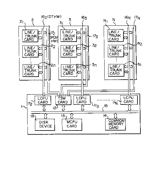
Fig. 1 shows a distribu-tion-controlled type private
branch exchange according to one embodiment of this inven-
tion which includes modules 1 to N packed in a case.
Module 1 is a common control module including a main CPU
(MCPU) card programmed for exchange processing, main-tain-
ance, etc., local CPU (LCPU) card for decoding an instruc-
tion issued from MCPU in-to control data corresponding to a
type of terminals used, and time switch (TSW) card for
perEorming data exchange processing between terminals.
Modules 2 to N are line/trunk modules connected -to stan-
dard telephones, digital multi-function telephones, data
terminals, etc.
Fig. 2 is a block diagram of modules 1 to N in
Fig. 1. Line/trunk modules 2, 3, ... N comprise line/
trunk cards 21 to 2n, 31 to 3m' 1 i
ly. To each of the line/trunk cards are connected a
plurality of terminals (standard telephones or digital
telephones) belonging to the same type.
Common control module 1 inc]udes LCPU cards 112 to
]lN corresponding to line/trunk modules 2 to N, TSW card
12, MCPU card 13, common mernory card 1~ and Eloppy disk
(hardware disk) device L8. C,CPU card 112 to llN, TSW card
12, MCPU card 13, common memory card 14 and disk device 18
are connected toyether via a common bus (Eor example, IEEE
796) 15. Line/trunk cards 21 to 2 of module 2 are con-
nected to corresponding LCPU card 112 via common control
data highway (DTHW) 162 and to TSW card 12 via cornmon PCM
highway (PCMHW) 17. Similarly, module 3 is connected to
correspondiny LCPU card 113 via common control highway 163
and to TSW card 12 via common PCM highway 173. Module N
is connected to LCPU card llN via common control highway
16N and to TSW card 12 via common PCM highway 17N. Con-
trol data transEer be-tween the respective line/trunk
module and the common control module is eEfected in a
serial form via the control data highway and speech data,
such as voice information, is transferred in a serial Eorm
via the PCM highway.
To the respective line/trunk card is coupled a plu-
rality of data terminals of the same type, i.e., standard
telephones or digital telephones. Fig. 3 is a block
diagram of -the line/trunk card for telephones. According
to this inven-tion, the line/trunk card includes port con-
troller (PC) 31 comprised of CPU 32 and RAM 33. Inter-
face LSI (large scale integrated circuit hereinafter
reEerred to as ILSI) is provided in line/trunk card and is
connected to corresponding LCPU card via the control high-
way. ~s in the case of the exis-ting line/trunk cards, LSI
(DTLSI) 351 to 35K Eor digital telephones are provided in
line/trunk card and a digital telephone 36 is coupled to
an output port via four lines: two lines ~Eor voice data
transmission and two for con-trol code transmission. ILSI
34 communicates with the corresponding LCPU card via the
control highway and con-trols a communica-tion between port
controller 31 and digital telephone 36. As will be se-t
:Eorth below, control data and program for controlling
telephones and of:Elce lines are loaded via the control
highway and I~SI 34 into R~M 33 in the line/trunk card.
FigO 4 is a block diagram oE LCPU cards 111 to llN
in common control module 1. In Fig. 4, ILSI 41 is oE
the same type as ILSI 34 in Fig. 3 and is connected ko
the respective line/trunk card ILSI via control hignway
16. As will be set forth above, ILSI is switched between
a master operation mode and a slave opera-tion mode by
an external control input. ILSI 41 in the LCPU card
operates in the master mode in which case control data
is ~ed to the line/trunk cards in synchronism with a
transition in time slots. On the other hand, ILSI in
each line/trunk card operates in the slave mode in which
the data is sent to the LCPU card within a time slot
alone which has been ex-ternally designated. Local CPU
42 is connected via local bus 43 to ILSI 41 so as to
control ILSI ~1. To local bus 43, local memory 44 is
connected which stores progra~m and data :Eor ope:rating
LCPU 42. The program and data are loaded into the memory
from disk device 1~ in Fig. 2.
LCPU 42 is connected to common bus 15 via buEEer
45. ~iEEerent addresses are allocated to local memory
44 and common memory card 14. When LCPU 42 gains access
to common memory card 14, if address decoder 46 detects
an address alLocated to the common memory card, buEfer 45
is enabled to connect local bus 43 to common bus 15. As
i8~3~
a result, LCPU 42 gains access to common memory card 1~.
Fig. 5 is a block diagrarn of MCPU card 13 of sub-
stantially the same conEiguration as the LCPU card in
Fig. 4. MCPU card 13 is comprised o~ MCPU 52, local bus
S3, local memory 5~, buffer 55 and address decoder 56.
Fig. 6 is a block diagram of the TSW card. In this
TSW card, time switches and time switch control 61 are
connected -to the PCM high~ays to effect switching com-
munication data from terminals under control of MCPU 13.
Address decoder 62 connected to common bus 15 detects an
access to time switch control 61, enabling bufEer 63 to
connect time switch control 61 in TSW card 12 to common
bus 15.
Fig. 7 is a block diagram oE the common memory card.
In the common memory card, common memory 71 is accessed
by MCPU card 13 and LCPU cards 112 to llN and, when
address decoder 72 connected to common bus 15 detects
an access to common memory 71, bufEer 73 is enabled,
allowing common memory 71 to be connected to common
bus 15.
An explanat.ion will now be made as to data transmis-
s.ion within common control module 1. This data transmis-
sion inc:ludes the transmission oE data, from the LCPU
cards to the MCPU ca:rd, which indicate status of ter-
minaLs collected by respective LCPU card 11 Erom the as-
sociated line/trunk cards and data oE call con-trol re-
quest information, such as dial digit inEormation and key
i3~
-- 10 --
inEormation of electronic type key telephones to MCPU
card 13; and transmission of data, Erom MCPU card 13
to the LCPU cards, which indicate terminal control data
resulting from exchange processing, such as a ringing
transmit, ringing receive or clearing acknowledge data.
The aforementioned data transmission is perEormed
through common memory card 14 commonly accessible by -the
respective CPU in common control module 1. Each LCPU
card writes information into common memory card 14, each
time inEormation indicating the status change (Eor exam-
ple, up and down oE a telephone handest) of a terminal
is received and, dial inEormation is received. MCPU card
13 periodically polls common memory card 14 and detects
the status variation of the terminals. IE calling
occurs, for example, at a certain terminal, MCP~ 13
detects corresponding data in common memory card 14 and
perEorms the processing for calling a corresponding ter-
minal. In a series of call processing routines, MCPU
13 accesses common memory card 14 when it requires data
stored in common memory 14 and when it requires data
written into the common memory card Erom the terminals
through LCPU. If, as a result of processing, any varia-
tion occurs with respect to data Eor controlling the
terminal, this control data is written into the common
memory card. On the other hand, respective LCPU also
periodically po]ls the common memory card 14 and detects
the variation of terminal control data or fresh data
contents.
~ system for transmitting control data in a serial
form will be explained with reEerence to Fig. 8. ~s
set out above, the types of terminals (distinction 'oe-
tween digital telephone and standard telephone) connectedto the respective line/trunk cards are so intially
determined that some line/trunk cards correspond to only
the digital telephones and that some llne/trunk cards
correspond to only the standard telephones. The control
data and program difEer in accordance with the type
of terminals. It is required that the control data and
program be loaded from the dlsk device in the common
control module in-to each of -the line/trunk cards. This
inven-tion is characterized in that common control data
and program are loaded Erom the side oE the common
control module collectively into a respec-tive group
of line/trunk cards to which are connected the same
type of terminals, such as digital telephones or
standard telephones. This system can markedly reduce
the programming time in comparison w:ith the case where
the control data and program are loaded one by one into
the line/trunk card.
Fig. 8 typically shows LCPU card 112 and line/trunk
module 2 in E'ig. 2. LCPU card 112 comprises LCPU 42 and
master ILSI 41 which opera-tes in the master [node for data
transmission. I,ine/trunk card 21 includes slave ILSI 34,
port controller 31 and line circuitry 35. The other
3:L
- 12 -
line/trunk cards 22 to 2m have the same conEiguration.
Line circuitry 35 corresponds to digital telephone LSIs
351 to 35K in Fig. 3. ILSI in line/trunk carcl operates,
as set out above, in the slave mode for data transmis-
sion. ILSIs 41 and 34 are constituted by an LSI havingthe same configuration and, as set forth above, and
switched in their operation mode by an external mode
designation input. The terminal will now be explained
below as being a digital telephone.
Control highway DTHW 1~2 has data output line 81
for transmitting control data Erom master ILSI 41 to a
slave ILSI in the respective line/trunk card, data input
line 82 Eor transmitting con-trol data Erom the respective
slave ILSI to the master ILSI 41, clock signal line ~3
for supplying a clock signal DHCLK from clock generator
85, and frame synchronizing signal line 84 Eor supplying
to the respec-tive slave ILSI a frame synchronizing signal
DHFS Eor deEining one Erame period oE time which signal
is generated by master ILSI 41 in response to the clock
signal.
Master ILSI 41 sends data onto data line 81 in
synchronism with a transi-tion in the time slots in one
Erame period oE time and receives data Erom respec-tive
slave ILSIs in response to the detection oE a header
in the data on data line ~2. Master ILSI 41 makes a
request-to-receive interruption to LCPU 42 in response
to the reception of that data.
P~ 3~
Slave ILSI is configured to send data onto data Line
82 only at an externally designated time slot in response
to frame s~nchronizing signal FS and clock signal CLKS.
Slave II.SI receives data upon the detection of a coin-
cidence between an address (LSI address) of -the slave
ILSI and an address of data received after the header
detection and makes a request-to-receive interruption -to
port controller 31. Port controller 31 reads received
data Erom a la-ter-described receiving register in the
slave II,SI in response to a request Eor recep-tion and
wri-tes the data into a corresponding digital telephone
LSI in line circuitry 35. Data from line circuitry 35 is
sent to port controller 31 which in turn sends it to
slave ILSI 34 where i-t is stored into a transmitting
register as se-t forth later. Then the slave ILSI sends
the contents of receiving register onto data line 82 in
the designated time slo-t.
Fig. 9 shows a schematic arrangement oE ILSI 3~
which is applied to the digital telephone in particular.
ILSI 3~ comprises transmitting/receiving control circuit
91 responsive to an address input peculiar to each LSI,
a group acldress input common to a plurality of LSIs to
which are connected to the terminals oE the same type,
-these address inputs being provided by back plate wirings
of ISI, to frame synchronizing signal D~IFS and to control
highway clock signal DHCLK; receiving register 92 for
receiving control data transmitted over data line 81;
- 14 -
transmitting regi.ster 93 for transmitting control data
onto data line 82; CPU interEace 9~; and bus 95 Eor
connection between -transmi-tting and receiving regis-ters
93 and 92 and interEace 94. Where an address Eield in
control data which is received by receiving register 92
indicates LSI address data allocated -to the correspond-
ing LSI, yroup address information showing a group to
which this LSI belongs, or general addressing informa-
tion, then transmi-tting/receiving control circuit 91
issues an interrup-tion signal to port controller 31~
In response to this signal, port controller 31 receives
data in a control field and control data Eield in the
received data through interEace 94.
Fig. 10 shows a Eormat of control data which is
transmitted over the control data highway DT~IW. The
data is transmitted in units of one Erame (50 bi-ts). As
shown in Fig. 9, one frame is comprised of a 2-bit
header, one-byte (eight-bits) address ~field, one-byte
control Eield and our--byte control data field. The
header has "10" bits, showing the start oE control data
transmitted over a control highway. The address field
has MSB two-bit addressing marker inEormation whereby a
distinction is made among an individual addressing, group
addressing and general addressing. As shown in Fig. 9,
the marker information "00" shows individual addressing
followed by the 6-bi-t LSI address informa-tion starting
with a bit of "0". Marker information "10" shows the
S3~
- 15 -
group addressing followed by six-bi~ group address
information starting wi-th "0". Marker information "11l'
shows general addressing in which case all -the ILSIs
unconditionally receive the same control data. In
a control field, the MSB of "0" is followed by data
indicating a port No. denoting the number of the DTLSs
351 to 35K. When -the MSB is "1", a control command is
followed. The control command contains a control code
showing, for example, a card damage display, CPU reset-
ting, general or individual down-loading of programs
Erom the control module into the line/trunk cards, etc.
The control data Eield is comprised of four bytes
in which the -first byte shows a type of control and the
remaining three bytes show control parame-ters.
Table 1 shows one example of control data loaded
from LCPU into the line/trunk card.
Table 1
T~PE PARAMETERS
_ _ __
LED CONTROL NUMBER, LIGHTING PATTERN, COLOR
AUDIBLE TONE CONTROL PITCH, CADENCE
MIC/SPEAKER CONTROL ON/OFF
Table 2 shows one example of control data transmitted
from the line/trunlc card to LCPU.
3~L
- 16 -
Table 2
TYPE P ATTERN
_ __
HOOK S5~ITC~I ON/OFF
DIAL DIGIT 0 - 9
FUNC'rION KEY KEY NUMBER l
In the line/trunk cardl received control data i5
temporarily stored in RAM 33 and CPU 32 sends control
data to that DTLSI designated by a port number.
The function of the control data transmission system
of this invention will be described below with reference
to Fig. 11.
As set forth above, a plurality oE line/trunk cards
are coupled to LCPU card l] -through control data highway
16. The same type of -terminals (digital telephones,
standard telephones or office lines) are connec-ted to -the
corresponding line/trunk card. In Fig. 11, a group ad-
dress #A i9 provided to a plurality of line/trunk cards
to WhiCh the standard telephones (STT) are coupled and a
group address 1~B is provided to a group of line/trunk
cards to which digital telephones (DTT) are coupled. LSI
address #1, #n, l~n-~l and ~n~m are provided to the respec-
tive line/trunk cards. During the individual addressing,
the respective line/-trunk card receives, only when ad-
dressed by LCPU card 11, control data Erom the LCPU card.During -the group addressing, on the other hand, a plu-
rality oE line/-trunk cards having a group address
3~
- 17 -
designated by the address field from LCPU card 11 simult-
aneously receives control data from -the LCPU card. Dur-
ing the general addressiny~ all the line/trunk cards
simultaneously receive the control data :Erom LCPU card 11.
F~ig. 12 shows a packet format used when the LCPU
card down-loads control data and program into the line/
trunk cards. In the con-trol. data :Eield of an intial one
frame of control da-ta a down-load initiation in.Eorma-tio.n
(one byte), inEormation o:E -the number oE bytes to be
transEerred TRB (one byte) and start address information
(2 bytes) are transmitted. The control data in the
control data Eield in succeeding control data frames,
the number oE which is determined by TRB, are sequential-
ly loaded in the RAM in the por-t controller. Down-load
terminate inEormation (one by-te), check sum data (one
byte) and data representing a packet number (two bytes)
are sent in the final contro:L data Erame.
The arrangement o tLS:[ in Fig. 9 will be explained
below with re:Eerence to Figs. 13, 1~ and 15 showing the
arrangements of receiving register 92 and control cir-
cuit 91, transmitting register 93, and CPU inte:rface 9~,
respectively.
As shown in Fi.g. 15, PC 31 and interface ~SI 33 are
connected to each other via data buses Do to D7. C:PU 32
in PC 31 sends an internal register address signal Ao to
A2 which is in turn decoded by decoder 151 into register
select signals Ro to R5. CPU 32 supplies a chip select
slynal CS, read control signal R~ and write control sig-
nal W~ to ILSI 33.
ReEerring to Fig. 13, a 49-blt shiEt register 130
ls provided which receives control data DHIN and clock
signal DHCLK from data highway DTHW. The MSs and LSs
of shiEt register 130 are denoted by Q48 and Q0, respec-
tlvely. The header "10" of the con-trol data is detected
by gate 131 whereby the output of gate 131 goes from a
logic 1 to a logic 0 level. The ou-tput of gate 131 is
coupled -through gate 132 to D input of D-type flip-flop
(F/F) 133 and clock signal CLK is supplied -to the clock
input of F/F 133. The output Q of F/F 133 feeds, due to
its variation Erom the logic 1 to -the logic 0 level, a
latch signal to registers 134 to 139 and interruption
signal or request--to-receive signal to CPU 32 of port
controller 31.
Selector 141 is provided which receives, at Eirst
inputs ~, address inputs LAo to L~4 peculiar to this ILSI
and, as second inputs B, group address inputs Mo to M3.
~it output Q46 of shiEt register 130 is coupled to the
select control input oE selector 14l which, when the
header of the control data is detected by gate 131, cor-
responds to MSB in the addressing distinction inEormation
in -the address field oE the control data. As shown in
Fig. 10, MSB is 0 for the individual addressing and MSB
is 1 for group and general addressings.
Selector 141 selects LSI address information LAo to
3~
-- 19 --
~A4 when its select con-trol input is at a 0 level and
group address inforrnation Mo -to M3 when its select con
trol inpu-t is at a 1 level. The outputs of selector 141
are coupled to first inpu-ts oE address compara-tor 142
and -t~le bit outputs Q43 to Q39 oE shiEt registers 130 are
coupled to second inputs of comparator 142. When -the
header oE data is detected, Q43 to Q39 outputs show five
bi-ts except for the MSB of address data in the address
Eield. As set forth above, -the MSB of address da-ta is
0 at all times. When an address coincidence is detected
by comparator 142, the output of comparator 142 goes
to a logic 170" level. The output oE comparator 142 and
outputs Q45 and Q44 oE shift register 130 are coupled to
gate 143, noting that the output Q45 shows the LSB of
addressing marker information when the header is detec-ted
and that the output Q44 shows the MSB oE address data
which is "0" at all times when -the header is detec-ted.
As a result, the outpu-t of gate 143 goes to a "1" level
at the group and individual addressing times. Output
Q46 and Q45 oE shift registers 130 and output of gate 145
are coupled to gate 144 and group address inEormation Mo
to M3 are coupled -to AND gate 145. The group address
information Mo - M3 is utilized as control information
Eor determining an operation mode of the ILSI and all
bits thereoE are se-t to 1 Eor the master operation mode.
Since the ILSI of the line/trunk card is set to the slave
mode, the output of ~ND gate 145 is alwa~s "0". The
3~
- 20 -
ou-tput oE gate 144 is 1 for generaly addressingO The
outputs of gates 143, 1~4 and 145 are coupled to NO~
gate 146 and the output of the NOR gate is coupled to
gate 146.
Registers 134 to 139 are coupled to outputs Q47
to Q0 o:E shift register 1.30 and data of eight bytes from
shift register 130 are latched at a time in response to
a latch signal of F/F 133. This is done when, after
the header has been detected, the general addressing
information, LSI address of its own or group address is
detected.
Register select signals Ro to R5, as well as chip
select signal CS and read control signal RD, are supplied
to gates 160 to 164. The output signals of gates 160
to 165 are sequentially applied to registers 134 -to 139.
As a result, data latched in reyisters 134 to 139 are
sequentially supplied to PC 31 via data buses Do to D7.
As set forth above, the LSI o:E the respective line/
trunk card uncondltionally receives control data from
LCPU at the time of general addressing and control data
from the LCPU card, at the time of indlvidual or group
addressing, in response to the detection oE the LSI
adclress or the group address.
ReEerring to Fig. 14, 50-bit transmitting shift
register 170 is shown whose inputs Dl and D2 are sup-
plied with "1" and "0" showing -the header and whose in-
puts D3 to D50 are coupled to the outputs oE eight-bit
3 r
-- 21 --
registers 171 -to 176. The outputs o:E registers 171 to
176 are coupled in common to da~a bus Do to D7. Registers
171 to 176 sequentially latch data which are supplied
via data bus .Erom ~C 31 in response to signals from
decoder 177 to which are supplied register selec-t signals
Ro to R5, chip selec-t signals CS and write control signal
WR. The data latched in registers 171 to 176 are located
into 50-bit shift register 170. The output data from
shift register 170 is sent out through output buffer
178 which is responsive to a transmit enable signal L/S.
Transmit enable signal L/S is generated by transmit enable
signal genera-tor 179 which are responsive to LSI address
signal LAo to LA4, clock signal DTCLK, frame synchronizing
signal DHFS and the output signal of AND gate 145 in
Fig. 13 for determining the master or salve opera-tion
mode. In the line/trunk card opera-ting in the slave
mode, transmit enable signal generator 179 is arranged
to produce the transmit enable signal L/S in a -time slot
specified by the LSI address within one Erame period oE
time. Transmit enable signal has a duration corresponding
to 50 clock pulses DHCLK during which the output data is
Eully sent out :Erom shiEt register 170.
As set forth above, according to this invention,
the control data can be loaded into the corresponding
line/-trunk cards Erom the respective LCPU in the common
control module and the same control data and program
can be down-loaded at a time into the line/trunk
- 22 -
cards belonging to the same group. Furthermore, data
can be unconditionally loaded into all the corresponding
line/trunk cards from the respective LCPU. The advant-
age of this arrangement is prominently manifested when
the system is buit up at the time of the installation
or at the time of the restoration of a failure oE the
system. That is, a time taken for programs, etcO, to
be loaded depends on -the number of the programs, not
on -the number of line/trunk cards.