Note : Les descriptions sont présentées dans la langue officielle dans laquelle elles ont été soumises.
"
~268~
-- 1 --
OUTPUT AMPLIFIER
BACKGROU~D OF THE INV~NTION
1. Field of the Invention.
The present invention relates to amplifiers
05 used at the end of an amplification signal path and,
more particularly, to amplifiers used for connecting
to a load device having an electrical characteristic
exhibiting resonances.
An amplifier used at the end of the signal
path in an amplification portion of an analog system
is usually connected to a load device which is to be
driven by signals larger in magnitude but more or
less following the signal waveform provided at the
beginning of the particular amplification portion of
the system upon which amplification is performed.
For a simple load device, this usually causes no
problem beyond having adequate power available at the
amplifier output to drive this load device as
directed by the amplified signal. For more complex
load devices, however, further measures may be needed
because of the complex electrical impedance
characteristics that such devices can exhibit.
A typical complex load device would be a
speaker, ranging from a hearing aid speaker to a
public address system ~peaXer. Such speakers have
electrical characteristics which depend not only on
the electrical materials present, but also the
~echanical construction of the load device and the
acoustical surroundings in which such a device is
placed. That is, the electrical impedance
characteristic of the device will reflect therein
mechanical structural resonances modified by, and
perhaps added to by, resonances arising as a result
31 ;~688.~
of the acoustical impedance faced by the speaker.
The occurrance of such resonances leads to uneven
performance across the frequency range in which the
system is to perform~
05 Improvement~ in these resonance
characteristics to reduce difference~ between
different parts of the operating frequency ~pectrum
of the system are usually obtained through the use of
negative feedback from the amplifier output to a
point earlier along the ampliier signal path.
Voltage feedback is commonly used, and in some
systems has been supplemented by current feedback.
The latter, however, has been obtained through
sensing the current passing through the load which
reduces the range of output voltage ov~r which the
load can be driven. Thus, an output amplifier is
desired, particularly in low supply voltage
situations, which can control resonances in the load
device without limiting the voltage range over which
such a device may be driven.
SUMM~RY OF THE INVE~TIO~
The present invention provides an output
amplifier having a first controlled current
controller at the amplifier input to the output of
which are connected ~he input6 of two other
controlled current controllers. The outputs of these
latter controllers are each connected through
impedances to the input of a further controlled
current controller which has its output connected to
the output of the first controlled current
controller. Such controllers are conveniently
implemented using bipolar transistors. A means for
limiting excursions of the signals in the amplifier
is also provided.
~ ~ 6 ~2 ~
Thus, according to the present invention there is pro-
vided an amplifier having an input and an output, said amplifier
comprising a first controlled current controller having an input
and an output such that current flowing at said ~irst controlled
current co~troller output is controlled in amount by signals
occurring on said first controlled current controller inpu-t, said
first controlled current controller input serving as said ampli-
fier input; a second controlled current controller having an
input and an output such that current flowing at said second con-
trolled current controller output is controlled in amount by sig-
nals occurring on said second controlled current controller
input, said second controlled current controller input being
electrically connected to said first controlled current con-
troller output, said second controlled current controller output
serving as said amplifier output; a third controlled current con
troller having an input and an output such that current flowing
at said third controlled current controller output is controlled
in amount by signals occurring on said third controlled current
controller input, said third controlled current controller input
being electrically connected to said first controlled current
controller output; a fourth controlled current controller having
an input and an output such that current flowlng at said fourth
controlled current controller output is controlled in amount by
signals occurring on said fourth controlled current controller
input, said fourth controlled current controller output being
electrically connected to said ~irst controlled current con-
troller output; and first and second feedback impedances each
having first and second terminating regions between which each
exhibits a selected impedance, said first and second feedback
impedance first terminating regions each being electrically con-
nected to said fourth controlled current controller input, said
first feedback impedance second terminating region being electri-
cally connected to said second controlled current controller out-
put, and said second feedback impedance second terminating region
being electrically connected to said third controlled current
controller output. Suitably said first controlled current con-
- 2a -
î~6~
troller is a voltage controlled current sink. Desirably said
first controlled current controller comprises a transistor means
having first and second terminating regions and having a control
region therein by which said first controlled current controller
transistor means is capable of being directed, through electrical
energization thereof, to effectively provide a conductive pa-th of
a selected conductivity between said first controlled current
controller transistor means first and second terminating regions,
said first controlled current controller transistor means control
region being electrically connected to said first controlled cur-
rent controller input and said first controlled current control-
ler transistor means first terminating region being electrically
connected to said first controlled current controller output, and
wherein said first controlled current controller further compri-
ses a first impedance having first and second terminating regionsbetween which it exhibits a selected impedance, said first con-
trolled current controller first impedance first terminating
region being electrically connected to said first controlled
current controller transistor means second terminating region and
said first controlled current controller first impedance second
terminating region being electrically connected to a first ter-
minal means adapted for connection to a first source of voltage.
In one embodiment of the present invention said second
and third controlled current controllers are each a current si~k
and said fourth controlled current controller is a current
source. Desirably said fourth controlled current controller com-
prises first and second transistor means each having first and
second terminating regions and having a control region therein by
which each is capable of being directed, through electrical en~r-
gization thereof, to effectively provide a conductive path of a
selected conductivity ~etween its first and second terminating
regions, said fourth controlled current controller first transis-
tor means control region and second terminating region being
electrically connected together and to a first terminal means
adapted for connection to a first current flow means, said fourth
- 2b -
~ ~ 6 ~ 8~ ~
controlled current controller second transistor means control
region being electrically connected to said first terminal means,
said fourth controlled c~lrrent control second transistor means
second terminating region serving as said fourth controlled cur
rent controller output, and wherein said fourth con~rolled cur-
rent controller further comprises first and second imepdance
means each having first and second terminating regions between
which each exhibits a selected electrical i~pedance, said fourth
controlled current controller first and second impedance means
first terminating regions each being electrically connected
together and to a second terminal means adapted for connection to
a first source of voltage, said fourth controlled current con-
troller first impedance means second terminating region being
electrically connected to said fourth controlled current con-
troller first transistor means first terminating region whichserves as said fourth controlled current controller input, said
fourth controlled current controller second impedance means sec-
ond terminating region being electricall~ connected to said
fourth controlled current controller second transistor means
first terminat~ng region. Preferably said second and third con-
trolled current controllers each comprise a transistor means hav-
ing first and second terminating regions and having a control
region therein by which each is capable of being directed,
through electrical energization thereof, to effectively provide a
conductive path of a selected conductivity between its ~irst and
second terminating regions, said second controlled current con-
troller transistor means being formed substantially identically
to said third controlled current controller transistor means,
said second controlled current controller transistor means con-
trol region serving as said second controlled current controllerinput, said third controlled current controller transistor means
control region ser~ing as said third controlled current con-
troller input, said second controlled current cont~oller transis-
tor means first terminating region serving as said second con-
trolled current controller output, and said third controlled cur-
rent controller transistor means first terminating region serving
- 2c -
~26~
as said third controlled current controller output, said second
controlled current controller transistor means second terminating
region and said third controlled current controller transistor
means second terminating region each being electrically connected
to a first terminal means adapted for connection to a first
source of voltage. Suitably said second and third controlled
current controller inputs are each electrically connected to said
first controlled current controller output through an amplifica-
tion means, said amplificatisn means having an input electrically
connected to said first controlled current controller output and
having an output electrically connected to each of said second
and third controlled current controller inputs, said amplifica-
tion means bein~ capable of providin~ signals at said amplifica-
tion means output which are substantially similar to signals pro-
vided at said amplification means input but of a larger magni-
tude.
In another embodiment of the present invention said
first controlled current controller comprises a transistor means
having first and second terminating regions and having a control
region therein by which said first controlled current controller
transistor means is capable of being directed, through electrical
energization thereof, to effectively provide a conductive path of
a selected conductivity between said first controlled current
controller transistor means ~irst and second terminating regions,
said first controlled current controller transistor means control
region being electrically connected to said first controlled cur-
rent controller input and said first controlled current control-
ler transistor means first terminating region being electrically
connected to said first controlled current controller output, and
wherein said first controlled current controller further compri-
ses a first impedance having first and second terminating regions
between which it exhibits a selected impedance, said first con-
trolled current controller first impedance first terminating
region being electrically connected to said first controlled
current controller transistor means second terminating region and
- 2d -
~ 2 6
said first controlled current controller first impedance second
terminating region being electrically connected to a first
terminal means adapted for connection to a first source o~
voltage. Suitably said fourth controlled current controller
comprises first and second transistor means each having first and
second terminating regions and having a control region therein by
which each is capable of being directed, through electrical
energization thereof, to effectively provide a conductive path of
a selected conductivity between its first and second terminating
regions, said fourth controlled current controller ~irst
transistor means control region and second terminating region
being electrically connected together and to a second terminal
means adapted for connection to a first current flow means, said
fourth controlle~ current controller second transistor means
control region being electrically connected to said second
terminal means, said fourth controlled current control second
transistor means second terminating region serving as said fourth
controlled current controller output, and wherein said fourth
controlled current controller output further comprises first and
second impedance means each having first and second terminating
regions between which each exhibits a selected electrical impe-
dance, said fourth controlled current controller first and second
impedance means first terminating regions each being electrically
connected together and to a third terminal means adapted for
connection to a second source of voltage, said fourth controlled
current controller first impedance means second terminating reg-
ion being electrically connected to said fourth controlled cur-
rent controller first transistor means first terminating region
which serves as said fourth controlled current controller input,
said fourth controlled current controller second impedance means
second terminating region being electrically connected to said
fourth controlled current controller second transistor means
first terminating region.
35In a further embodiment of the present invention said
fourth controlled current controller comprises first and second
- 2e -
transistor means each having first and second terminating regions
and having a control region therein by which each is capable of
being directed, through electrical energization thereof, to
effectively provide a conductive path of a selected conductivity
between its first and second terminating regions, said ~our-th
controlled current controller first transistor means control
region and second terminating region being electrically connected
together and to a first terminal means adapted for connection to
a first current flow means, said fourth controlled current con-
troller second transistor means control region being electricallyconnected to said first terminal means, said fourth controlled
current control second transistor means second terminating region
serving as said fourth controlled current controller output, and
wherein said fourth controlled current controller further com-
prises first and second impedance means each having first andsecond terminating regions between which each exhibits a selected
electrical impedance, said fourth controlled current controller
first and second impedance means first terminating regions each
being electrically connected together and to a second terminal
means adapted for connection to a first source of voltage, said
fourth controlled current controller first impedance mea.ns second
terminating region being electrically connected to said fourth
controlled current controller first transistor means first termi-
nating region which serves as said fourth controlled current con-
troller input, sald fourth controlled current controller secondimpedance means second terminating region being electrically con-
nected to said fourth controlled current controller second tran-
sistor means first terminating region. Suitably a supplementary
impedance means having first and second terminating regions
between which lt exhibits a selected impedance, said supplemen-
tary impedance first transmission reyion being electrically con-
nected to said second terminal means, and said supplementary
impedance second terminating region being electrically connected
to said third controlled current controller output. Alterna-
tively a supplementary impedance means having first and secondterminating regions between which it exhibits a selected
- 2~ -
impedance, said supplementary impedance first transmission regionbeing electrically connected to said second controlled curren-t
controller output, and said supplementary impedance second termi-
nating region being electrically connected to said third con-
trolled current controller output.
In another embodiment of the present invention saidsecond and third controlled current controllers each comprise a
transistor means having first and second terminating regions and
having a control region therein by which each is capable of bein~
directed, through electrical energization thereof, to effectively
provide a conductive path of a selected conductivity between its
first and second terminating regions, sald second controlled cur-
rent controller transistor means being formed substantially iden-
tically to said third controlled current controller transistormeans, said second controlled current controller transistor means
control region serving as said second controlled current con-
troller input, said third controlled current controller transis-
tor means control region serving as said third controlled current
controller input, said second controlled current controller tran-
sistor means first terminating region serving as said second con-
trolled current controller output, and said third controlled cur-
rent controller transistor means first terminating region serving
as said third controlled current controller output, said second
controlled current controller transistor means second terminatlng
region and said third controlled current controller transistor
means first terminating region each being elPctrically connected
to a first terminal means a~apted for connection to a second
source of voltage. Suitably said second and third controlled
current controller inputs are each electrically connected to sald
first controlled current controller output through an amplifica-
tion means, said amplification means having an input electrically
connected to said first controlled current controller nutput and
having an output electrically connected to each of said second
and third controlled current controller inputs, said amplifica-
tion means being capable of providing signals at said amplifica-
- 2g -
tion means output which are substantially similar to signals pro-
vided as said amplification means input but of a larger magni-
tude.
In another embodiment of the present invention sald
second and third controlled current controller inputs are each
electrically connected to said first controlled current con-
troller output through an amplification means, said amplification
means having an input electrically connected to said first con-
trolled current controller output and having an output electrl-
cally connected to each of said second and third controlled cur-
rent controller inputs, said amplification means being capable of
providing signals at said amplification means output which are
substantially slmllar to slgnals provlded at sald amplificatlon
means lnput but of a larger magnitude. Suitably a load device is
connected between said ampllfler output and a flrst terminal
means adapted for connection to a second source of voltage.
Desirably there ls provided a supplementary impedance means hav-
lng first and second terminating regions between which it
exhibits a selected impedance, said supplementary impedance first
terminating region being electrically connected to said second
controlled current controller output, and said supplementary
impedance second terminating region bein~ electrically connected
to said third controlled ~urrent controller output. Sultably
there is further provlded a signal excursion control means whlch
senses signal levels occurring at said fourth controlled current
controller input and, for signals exceeding a selected level,
alters electrical conditions at said first controlled current
controller input.
In a further embodlment of the present inventlon said
second and third controlled current controllers earh comprlse a
transistor means having first and second termlnatlng regions and
havlng a control region thereln by which each is capable of being
directed, through electrical energization thereof, to effectively
provide a conductive path of a selected conductivlty between its
- 2h -
32~
first and second terminating regions, said second controlled cur
rent controller transistor means being formed substantially iden-
tically to said third controlled current controller translstor
means, said second controlled current controller transistor means
control region serving as said second controlled current control-
ler input, said third controlled current controller transistor
means control region serving as said third controlled current
controller input, said second controlled current controller
transistor means first terminating region serving as said second
controlled current controller output, and said third controlled
current controller transistor means first terminating region
serving as said third controlled current controller output, said
second controlled current controller transistor means second
terminating region and said third controlled current controller
transistor means second terminating region each being electri-
cally connected to said first terminal means.
The present invention will be further illustrated by
way of the accompanying drawings:-
- 2i -
-- 3 --
BRIEF DESCRIPTION OF THE DRAWI~GS
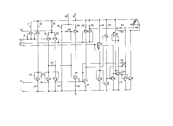
Figure 1 is a schematic diagram of the
present invention.
DETAILED DESCRIPTION OF THE PREFERRED EMBODIME~TS
05Figure 1 shows a schematic diagram of an
output amplifier suitable for use with a low voltage
power supply in monolithic integrated circuit form~
This amplifier has an input, 10, with respect to a
ground reference voltage terminal, 11~ Input 10 is
connected through a resistor 12, to the base of an
input npn bipolar transistor, 13. The emitter of
transistor 13 is electrically connected through a
resistor, 14, to ground reference terminal 11. Thus,
the current drawn at the collector of transistor 13
is set by the voltage on input 10 and by the bias
current supplied at the base thereof to be described.
Bias current is supplied to transistor 13 at
its base through resistor 12 by means of a current
source and a reference transi~tor. The current
souxce is formed by two pnp bipolar transistors, 15
and 16, each of which is connected through an emitter
resistor, 17 and 18, respectively, to a positive
voltage supply terminal, 19, adapted for connection
to a source of positive voltage such as a battery.
The base of transistor 16 is connected to a further
terminal means, 20, adapted for connection to a first
current sink which sinks a well regulated current.
The base of transistor 15, through a further
resistor, 21, is also connected to terminal 20 as i~
the collector of transistor 15.
Transistors 15 and 16 are closely matched as
are resistors 17 and 18. As a result, the current
~2~ 6
-- 4 --
sunk by the regulated current source connected to
terminal 20 will be primarily supplied by the
collector of transistor 15, although a slight portion
of it will be due to the bases of the various
05 transistors connected to terminal 20. ~ nearly
identical current will flow from the collector of
transistor 16 as the base and emitter of transistor
16 are in electrical conditions very similar to the
base and emitter of transistor 15. Resistors 17 and
18 help stabilize the currents in each of transistors
and 16 over changing circuit conditions in
operation, reduce the effects of any mismatching
between transistors 15 and 16, and raise the
effective output impedance occurring at the collector
of transistor 16.
The collector curxent of transistor 16 is
supplied to the collector of a further npn bipolar
transistor, 22. A slight amount of the current from
the collector of transistor 16 is provided to the
base of transistor 22 through a further resistor, 23.
These currents are carried through transistor 22 out
its emitter, and then through a further resistor, 24,
electrically connected to ground reference terminal
11. Resistor 24 helps stabilize the voltage at the
collector of resistor 22. That collector is
connected through another resistor, 25, to the base
of transistor 13 through resistor 12 to thereby
supply a base bias current.
The current to the collector of transistor
13 is provided by two sources, a controlled current
source and the input of the next amplification
stage. The controlled current source is formed by a
pair of pnp bipolar transistors, 26 and 27, and a
x~
corresponding pair of re~istors, 28 and 29,
respectively, each electxically connecting the
corresponding emitters to voltage supply terminal
means 19. As in the previously described current
05 source, the base and collector of transistor 27 are
each electrically connected to a further terminal
means, 30, which is connected to another current sink
which sinks a well regulated current. Again, this
current is primarily supplied by the collector of
transistor 27, although, again, a slight portion is
supplied by the transistor ba3es connected to
terminal 30. Since tran~istors 26 and 27 axe well
matched to one another, as are resistors 28 and 29,
and since the base of transistor 26 is also connected
to terminal 30, the collector of transistor 26 will
provide a current essentially identical to that
supplied by the collector of transistor 27. This
collector current of transistor 26 can be altered
because of the incoming connection at the junction of
2Q transistor 27 and resistor 29, as will be described
later.
Again, resistors 28 and 29 stabilize the
current supplied by this current source under
changing circuit conditions, reduce the effects of
any mismatching between transistors 26 and 27, and
raise the effective impedance at the collector of
transistor 26. Further, if the transistors used to
make up this current source happen to have low
current gains, there can be an increaq~ in the
voltage at the emitters of transistors 26 and 27.
Resistors 21 and 23 approximately compensate for this
effect.
~26~
The other current drawn at the collector of
transistor 13 is supplied from the base of a pnp
bipolar transistor, 31, having its emitter
electrically connected through a resistor, 32, to
05 positive voltage supply terminal 19. The collector
load of transistor 31 i5 formed by an npn bipolar
transistor, 33, serving as a current sink. The
current value to be sunk at the collector of
transistor 33 and passed through its emitter to
ground reference terminal 11 is set by a
diode-connected npn bipolar transistor, 34. The
collector of transistor 34 is electrically connected
to its base and to the base of transistor 33. The
emitter of transistor 34 is electrically connected to
ground reference terminal 11.
The base and collector of transistor 34 are
supplied current from a multiple collector pnp
bipolar transistor, 35, having its emitter connected
through a resistor, 36, to positive voltage supply
terminal 19. Transistor 35 will operate as a current
source in much the same manner as the current source
formed by transistors 26 and 27. The base of
transistor 35 is connected to a terminal means, 37,
which is adapted for connection to a well regulated
current sink. Transistor 35 has four separate
collectors, two of which are electrically connected
together and to the base of transistor 35. In this
arrangement, the other two collectors will each
supply approximately the same current as one of the
collectors shorted to the base of transistor 35, each
of the collectors being matched in construction to
the others.
~6~8~6
A voltage signal impressed on amplifier
input 10, then, will change the current value to be
sunk at the collector of transistor 13. This change
in current value must be satisfied by changes in the
05 current supplied by the collector of transistor 26
and the base of transi~tor 31. Changes in ~he base
current of transistor 31 are amplified by the
remaining portions of the amplifier to its output,
and changes at the output are reflected through a
feedback arrangement to provide changes in the
current supplied by the collector of transi~tor 26,
as will be explained below.
The portion of ths current required to be
sunk at the collector of transistor 33, which is not
supplied by transistor 31, must be supplied by the
base of a further pnp bipolar transistor, 38, which
has its emitter electrically connected to the
remaining collector of transistor 35. Also
electrically connect~d to the emitter of transistor
38 is the base of a further npn bipolar tran~istor,
39, and a collector of another multicollector pnp
bipolar tran~istor, 40, serving as a controlled
current source~ The emitter of transistor 39 is
electrically connected through a resistor, 41, to
ground reference terminal 11. The emitter of
tranqistor 40 is directly electrically connected to
positive voltage supply terminal 19. The collector
of transistor 39 is electrically connected to one of
the two collectors of transistor 40, which collector
is also electrically connected to the base of
transistor 40. Finally, the base of transistor 39 is
also electrically connected to the base of an output
npn bipolar transistor, 42, through a resistor, 43.
Current is supplied by the last-mentioned
collector of transistor 35 to the emitter of
transistor 38, to the base of transistor 39 and
through resistor 43 to the ba~e of transistor 42~
05 The current in the base of transistor 39, varying in
response to input signals, causes a variable
collector current to be drawn thereby which must be
supplied by the collector of transistor 40 to which
it is connected and to a slight extent by the base of
transistor 40. This causes substantially identical
currents to be provided at the other collector o~E
transistor 40 which is supplied, as previously
indicated, to the emitter oE transistor 38, the base
oE transistor 39, and the base of transistor 42
through the resistor 43. The extent of this positive
feedback action is limited, however, by the presence
of resistor 41 in the emitter of transistor 39. As
an increasing voltage is dropped thereacroqs because
of increasing emitter current in transistor 39, a
much larger current is provided to the base of
tran~istor 42 until the voltage at the base of
tran~istor 39 is effectively damped by the
base-~o-emitter voltage of transistor 42. Greater
current supplied at the base of transistor 39 by
transistor 40 is thereafter increasingly shunted by
transistor 3~ Erom the base of transistor 39.
The much larger current supplied by the
collector of transistor 40 ~o the base of transistor
42 through resistor 43 is the ~oost current used to
drive transister 42 to provide the amplifier load
current. The emitter oE transistor 42 is connected
to ground reference terminal 11 while the collector
of transistor 42 is connected to that terminal of the
amplifier ~erving as an output, 44. Terminal 44 has
~26~ 6
_ g _
shown electrically connected thereto a load device
the other end of which is electrically connected to
positive supply terminal 19.
This load device is shown to be pri~arily
05 inductive in the symbol used therefor in Figure 1,
but this is not necessarily the impedance
characteristic of possible loads but rather a typical
characteristic. Note that no other impedance means
is connected between ground reerence terminal 11 and
positive supply means 19 other than this load device
and the emitter to collector portion of transistor 42.
The portion of the current from the
collector of transistor 40 which drives the base of
transistor 42 is determined by the values of
resistors 41 and 43 and by the emitter area of
transistor 42 relative to that of transistor 39. A
typical area ratio would be to have the emitter area
of transistor 42 sixteen times that of transistor 39.
Resistor 43 also serves to increase the proportion
should transistor 42 have a relatively low current
gain. The emitter area for transistor 38 must be
chosen so that the base-to-emitter voltage drop of
transistor 33 does not exceed that of transistor 42
so that it can always be capable of drawing current
rom the collector of transistor 40 connected
thereto. This allows transistor 42 to have an
extremely low current provided thereto to permit a
full output transistor operating range.
The voltage developed at amplifier output
44, acrosq the load device, is fed back through a
resistor, 45, to the junction of resistor 29 and the
emitter of transistor 27. The voltage at amplifier
output 44, as a result, changes the current drawn
through resistor 29 thereby changing the voltage
3826
-- 10 --
occurring at the emitter of transistor 27. Since the
currents through transistor 27 are ~et by the
regulated current source connected to terminal 30,
the voltage a~ the base and collector of transistor
05 27 must change by a 3imilar amount, which change also
occurs on the base of transistor 26. The change in
voltage on the base of transistor 26 will, since the
emitter-to-base voltage of transistor 26 is
relatively constant, be reflected in the drop across
resistor 28 which must primarily be re1ected in the
change in the collector current of transistor ~6.
'Fhus, as indicated above, a signal on
amplifier input 10 leading to a change in the current
drawn at the collector of transistor 13 will be
balanced by two changes. There will be a change in
the current drawn from the input of the amplification
arrangement between transistor 13 and output 44,
leading to this change being amplified at amplifier
output 44, and a change in the current supplied by
the current ~ource containing transistor 26 because
of feedback from amplifier output 44 reflecting the
change there.
The feedback provided by resistor 45 is
essentially feedback based on the voltage drop across
the load device connected between amplifier output 44
and positive supply voltage terminal 19. This
voltage drop is used to essentially set the current
drawn through resistor 45 to control the current
supplied at the collector of transistor 26 to the
collector of transistor 13.
This voltage feedback, however, is often not
sufficient to reduce the resonances which would occur
in the circuit of Figure 1. To more fully reduce the
variance in the frequency spectrum characterizing the
.
12~ 3Z6
circuit of Figure 1 due to such resonances, the
addition of current feedback is provided through the
use of a further npn bipolar transistor, 46, having
its emitter electrically connected to ground reference
05 terminal 11, and another 4eedback resistor, 47.
Transistor 46 is a transistor which substantially
matches the construction used in transistor 42, but
like transistor 39 has an emitter area which is only
one sixteenth that of transistor 42. The base of
transistor 46 is electrically connected to the base
of transistor 42 so that it receives essentially the
same drive current as does transistor 42. As a
result, the collector current drawn by transistor 46
will be substantially a fixed fraction of that drawn
by transistor 42 so that its current repre~ents the
load current drawn by transistor 42 as a basis for
providing current feedbac~. Such feedback requires
that a resistor be placed from the collector of
transistor 46 at a terminal connection thereto, 48,
to either amplifier output 44 or positive voltage
supply terminal 19. Such resistors are shown in
dashed line form in Figure 1~ The signal from
terminal 48 is then fed back through re~istor 47 to
the same junction of resistor 29 and the emitter of
transistor 27 as is the signal through resistor 45.
The use of transistor 46, with its collector
current repre~enting the load current flowing in
transistor 42, in place of having a sense resistor in
series with transistor 42 and the load device means
permits the full output voltage range to be applied
to the load device. There is no voltage change
limitation for the load device connected to amplifier
output 44 because of any series voltage drop due to a
sensing element. Thus, in low voltage applications
' `'"' '" ' `" '
~2,6~3B~6
- 12 -
where the voltage on positive supply terminal 19 is
quite small so that the voltage loss to a sensing
resistor would be signific~nt, an output voltage
range reduction is avoided by the arrangement of
05 Figure 1.
The signal excursion limiting circuitry is
shown in Figure 1 to the le~t of transistor 13. A
pair of pnp bipolar transistors, 49 and 50, each ha~e
a resistor electrically connected to the emitter
thereof, 51 and 52, respectively. The other side of
each of resistors 51 and 52 are electrically
connected together and are connected to positive
voltage supply terminal 19 through another resistor,
53. Transistors 49 and 50 each have an npn bipolar
transistor, 54 and 55, respectively, as a current
source load. These transistor pairs each have
members which are well matched. Each of transistors
54 and 55 has its base connected to the collector of
transistor 54 so that transistor 54 is a diode
connected transistor. Since each of transistors 54
and 55 are matched and have t~e bases connected to
the same point, each will sink essential~y the same
current therethrough to ground terminal reference 11
electrically connected to the emitters of each of
these transistors.
The base of transistor 49 is electrically
connected to terminal 20 adapted, as stated before,
for connection to a well regulated current sink.
Likewise, the base of transistor 50 is connected to
terminal 30 which is also adapted for connection to a
well regulated current sink, and which is a current
sink which will draw the same current as that
connected to terminal 20. Thus, similar condi~ions
will occur at the bases of each of transistors 51 and
52 except for the feedback connection through
resistoxs 45 and 47 which cause voltage differences
between terminal 30 and terminal 20. Such differences
in voltage between terminals 20 and 30 will lead to a
05 differential voltage at the bases of tranæistors 51
and 52 resulting in a voltage change at the collector
of transistor 50.
The collector of tran~istor 50 is
electrically connected to the bases of two further
transistors, S6 and 57. Transistor 56 is a pnp
bipolar transistor connected through a resistor, 58,
to an electrical terminal means, 59, adapted for
connection to a source of well regulated positive
voltage. Transistor 57 has its emitter connected
through a further resistor, 60, to ground reference
terminal 11. The collector of transistors 56 and 57
are electrically connected together and to the base
of transistor 13.
The bases of transi~tors 56 and 57 are also
connected to a voltage divider network provided by a
pair of resistors, 61 and 62, connected in series
between regulated positive voltage terminal 59 and
ground reference terminal 11. At the junction of
these two resistors, a further resistor, 63, is
electrically connected to both of the bases of
transistors 56 and 57. These resis~ors, 61, 62 and
63, set the bias conditions on the bases of these
transistors and are chosen, along with the regulated
voltage value on terminal 59 and the threshold valu~s
of transistors 56 and 57, such that transistors 56
and 57 are not in the conducting condition in the
quiescent state. However, a sufficient shift in
voltage at the collectors of transistors 50 and 55
will lead to sufficient changes in the basss of
9"2~ 6
- 14 -
transistors 56 and 57 to cause one or the other of
them to conduct to thereby reduce the signal at the
base of transistor 13.
A further terminal means, 64, is connected
05 to the junction of resistors 51, 52 and 53 to permit
eliminating the excursion limiting circuit from
acting at all, or to permit varying levels of signal
excursion limitation. This can be accomplished by
connecting terminal 64 to ground reference terminal
11, to positive voltage supply terminal 19, or
through a resistor to either.
Three capacitances, 65, 66 and 67, are used
specifically in the circuit of Figure 1. Capacitance
65 prevents overshoot from occurring during operation
of the signal excursion limiting circuit just
described. Capacitance 66 provides a frequency
characteristic rollofE for the entire amplifier for
frequencies past the range of normal hearing if used
with a speaker as a load device. Capacitance 67
provides a frequency characteristic rolloff for the
current boost portion of the circuitry described
above. The capacitances are all formed as parallel
plate capacitors in the monolithic integrated circuit
chip in which the circuit of Figure 1 is formed
~excluding the load means and possibly excluding a
resistor between terminal 48 and either of terminals
44 or 19).
The npn bipolar transi~tors used in the
circuit of Figure 1 all have the same constructional
design and reasonably match one another with the
exception of differences in emitter areas as already
described. Similarly, the pnp bipolar transistors
are all constructed the same in the monolithic
integrated circuit with the exception of the number
12~ 6
- 15 -
of collectors, as already described. Thus, the npn
bipolar transistors reasonably match one another
outside the corresponding exception, and the pnp
bipolar transistors also reasonably match one another
05 outside the exception corresponding thereto~ The
resistors in the circuit are formed by ion
implantation in the monolithic integrated circuit
chip. For a typical bipolar integrated circuit
fabrication process, the capacitances miyht have
values of 15 pf for capacitance 65, and 33 pf for
each o~ capacitances 66 and 67. The resi6tors might
be chosen to have the ~ollowing resistance values in
ohms:
ResistorsResistance Values
1216,000
1416,000
1716,000
1816,000
216,000
2374,000
2416,000
2516,000
2816,000
2916,000
3232,000
368,000
412,000
431,500
45160,000
47160,000
5132,000
5232,~00
5364,000
5816,000
6016~000
6164,000
6264,000
63100,000