Note : Les descriptions sont présentées dans la langue officielle dans laquelle elles ont été soumises.
MULTILEVEL MODULATOR CAPABLE OF PRODUCING A COMPOSITE
MODULATED SIGNAL COMPRISING A QUADRATURE AMPLITUDE
MODULATED COMPONENT AND A PHASE MODULATED COMPONENT
Background of the Invention:
This invention relates to a multilevel modulator
capable of producing a composite modulated signal in
response to a main data signal and a subdata signal and
5 to a multilevel demodulator for use as a counterpart of
the multilevel modulator.
A multilevel modulating system of the type
described is exemplified in United States Patent No.
4,498,050 issued February 5, 1985, to Yasuharu Yoshida,
10 the instant applicant, and assigned to NEC Corporation.
This system is a composite PSK-PSK modulating system
which comprises a 2k-phase PSK modulated compon~nt
carrying the main data signal and a 2-phase PSK
modulated component carrying the subdata signal where k
15 represents a positive integer. In the system, the main
data signal has a first bit rate fl which is not less
than a second bit rate f2 of the subdata signal. As a
~,
68~
2 64768-142
result, the su~data signal can be effectively transmitted without
adversely affecting a bit error rate of the main data signal.
In the meanwhile, a multilevel quadrature amplitude
modulating system has recently become the center of a digital
transmission sys~em. In the multilevel quadrature amplitude
modulating system, a pair of quadrature-phase carrier signals are
amplitude modulated by first and second input signals into a
multilevel quadrature amplitude modulated signal. When each of
the first and the second input signals is an n-bit binary signal
where n is a positive integer which is not less than two, the
multilevel quadrature amplitude modulated signal has 22n output
signal points on a phase plane which has an origin and real and
imaginary axes orthogonally crossing at the origin. Such a
multilevel quadrature amplitude modulator is exemplified in
Canadian patent No. 1,251,526 issued March 21, 1989, by Junichi
Uchibori et al, assigned to NEC Corporation.
The multllevel quadrature amplitude modulator can
effectively utilize a carrier level. There~ore a large-capacity
digital radio communication network ordinarily comprises the
multilevel quadrature amplitude modulator.
By the way, the conventional composite modulatiny system
is restricted to the PSK modulation. Namely, the conventional
composite modulating system can
~Z~ 8
not be applied to the multilevel quadrature amplitude
modulating system.
5ummary of the Invention:
It is therefore an object of this invention to
5 provide a multilevel modulator capable of producing a
composite modulated signal comprising a quadrature
amplitude modulated component and a phase modulated
component in response to a main data signal and a
subdata signal each o~ which has different bit rates and
10 which are supplied to the modulator as input signals.
It is another object of this invention to
provide a multilevel demodulator which is for use as a
counterpart of the multilevel modulator of the type
described above.
A multilevel modulator to which ~his invention is applicable
is for modulating first and second main data signals and
a subdata signal into a composite modulated signal.
Each of the first and the second main data signals is
represented by first through n-th bits where n is a
20 positive integer which is not less than two. The
subdata signal is represented by one of first and second
binary values at a time. The multilevel modulator
comprises modulating means responsive to the first and
the second main data signals and the subdata signal for
25 modulating the first and the second main data signals
and the subdata signal into the composite modulated
signal comprising a quadrature amplitude modulated
component and a phase modulated component. The
3X~
quadrature amplitude modulated component is modulated by
the first and the second main data signals and has 22n
output signal points on a phase plane. The phase
modulated component is modulated by the subdata signal.
A multilevel demodulator to which this invention
is applicable is for demodulating a composite modulated
signal comprising a multilevel quadrature amplitude
modulated component modulated by first and second main
data signals and a phase modulated component modulated
10 by a subdata signal. Each of the first and the second
main data signals is represented by first through n-th
bits and has a first bit rate fl. The subdata signal is
represented by one of first and second binary values at
a time and has a second bit rate f2 which is not greater
15 than the first bit rate divided by a predetermined
natural number m. The phase modulated component has a
-
phase difference of 2~ radian when the subdata signal is
represented by a predetermined one of the first and the
second binary values where ~ is not greater than ~/22n.
20 The multilevel demodulator comprises detecting means for
phase detecting said composite mcdulated signal to
produce first and second phase detection signals.
According to this invention, the multilevel demodulator
further comprises reproducing means coupled to the
25 detecting means for reproducing a reproduced subdata
signal and first and second reproduced main data signals
in response to the first and the second phase detection
signals.
, ::
In the manner which will later be illustrated,
the amplitude modulated component is represented on a
phase plane by a radius from an origin. 'rhe phase
modulated component is represented by a clockwise or a
5 counterclockwise shift.
Brief Description of the Drawing:
Fig. 1 is a block diagram of a multilevel
modulator according to a first embodiment of this
invention;
Fig. 2 shows an output signal point arrangement
of a composite!modulated signal produced by the
multilevel modulator illustrated in Fig. l;
Fig. 3 is a block diagram of a multilevel
modulator according to a second embodiment of this
15 invention;
Fig. 4 is a block diagram of a multilevel
demodulator for use as a counterpart of the multilevel
modulator illustrated in Fig. l;
Fig. 5 is a block diagram of a subdata producing
20 circuit and a selecting unit operable as a part of the
multilevel demodulator illustrated in Fig. 4;
Fig. 6 is a block diagram of a multilevel
demodulator according to another aspect of this
invention;
Fig. 7 is a block di-agram of a subdata
reproducing circuit operable as a part of the multilevel
demodulator illustrated in Fig. 6;
~268~
Fig. 8 is a view for use in describing operation
of the subdata reproducing circuit illustrated in
Fig. 7;
Fig. 9 is a block diagram of a multilevel
5 demodulator according to still another aspect of this
invention;
Fig. 10 is a block diagram of a subdata
reproducing unit operable as a part of the multilevel
demodulator illustrated in Fig. 9;
Fig. 11 is a view for use in describing
operation of the subdata reproducing unit illustrated in
Fig. 10;
Fig. 12 is a view for use in describing
operation of the subdata reproducing unit illustrated in
15 Fig. 10;
Fig. 13 is a block diagram of another subdata
reproducing unit operable as a part of the multilevel
demodulator illustrated in Fig. 9;
Fig. 14 is a block diagram of a main data
20 reproducing unit operable as a part of the multilevel
demodulator illustrated in Fig. 9; and
Fig. 15 is a view for use in describing
operation of the main data repxoducing unit illustrated
in Fig. 14.
Description of the Preferred Fmbodiments:
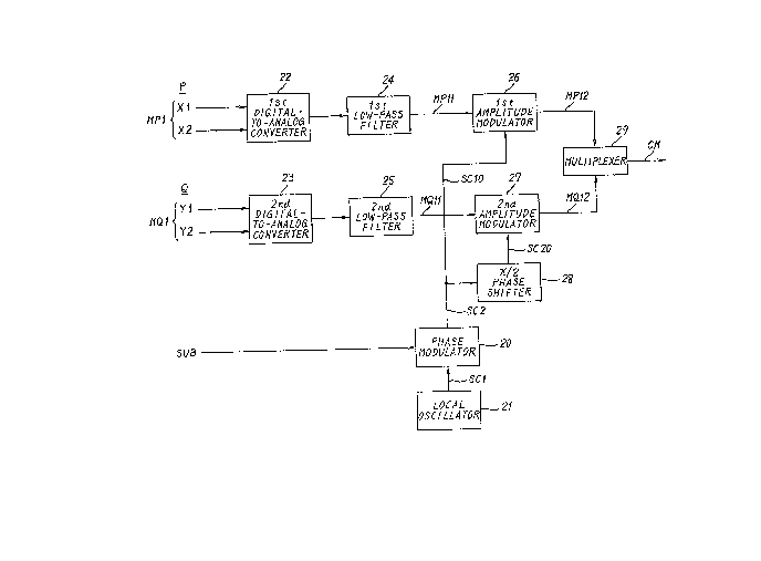
Referring to Fig. 1, a multilevel modulator
according to a first embodiment of this invention is
similar to a conventional four-by-four quadrature
:~X~i~38;~
amplitude modulator except for a phase modulator 20.
The multilevel modulator is for use in modulating first
and second main data signals MPl and MQl and a subdata
signal SUB into a composite modulated signal CM. Each
5 of the first and the second main data signals MPl and
MQl is represented by n bits where n represents a
positive integer which is not less than two.
Ordinarily, the n bits are processed in bit parallel.
It will be assumed merely for brevity of description
10 that the positive integer is equal to two.
It will be assumed that the first main data
signal MPl is of a channel P and is represented by first
and second bits ~1 and X2. The second main data signal
MQl is of another channel Q and is represented by first
15 and second bits Yl and Y2. Each of the first and the
second main data signals MPl and MQl is therefore
capable of representing four levels. Each of the first
and the second main data signals MPl and MQl has a first
bit rate fl. The subdata signal SUB is represented by a
20 single bit, namely, one of first and second binary
values which may be binary values "1" and "0". The
subdata signal SUB has a second bit rate f2 which is
equal to fl/m where m is a positive integer which is not
smaller than two.
The phase modulator 20 is supplied with a
carrier oscillation signal SCl from a local oscillator
21 and is supplied with the subdata signal SUB. The
phase modulator 20 is for phase modulating the carrier
oscillation signal SCl by the subdata signal SUB and
produces a phase modulated signal SC2. For example, the
phase modulated signal SC2 has a first predetermined
phase difference relative to the carrier oscillation
5 signal SC1 when the subdata signal SUB has the binary
value "0". When the subdata signal SUB has the binary
value "1", the phase modulated signal SC2 has a second
predetermined phase difference relative to the carrier
oscillation signal SCl. The first and the second
10 predetermined phase differences should have a common
absolute value ~ which should not be greater than ~/22n
radian. In the example being illustrated, 0~19 radian
is selected as the common absolute value ~.
The multilevel modulator comprises a first
15 digital-to-analog converter 22 supplied with the first
main data signal MPl and a second diqital-to-analog
converter 23 supplied with the second main data signal
MQl. The first digital-to-analog converter 22 converts
tAe first main data signal MPl to a first analog signal.
20 The second digital-to-analog converter 23 converts the
second main data signal MQl to a second analog signal.
Each of the first and the second analog signals has an
amplitude level determined by a pertinent one of the
first and the second main data signals MPl and MQl. The
25 first and the second analog signals are delivered
through first and second low-pass filters 24 and 25 to
first and second amplitude modulators 26 and 27 as first
and second modulating signals MPll and MQll,
respectively.
The phase modulated signal SC2 is delivered to
the first amplitude modulator 26 as a first carrier
5 signal SC10 and supplied through a ~/2-phase shifter 28
to the second amplitude modulator 27 as a second carrier
signal SC20, The first carrier signal SC10 has a
quadrature phase difference relative to the second
carrier signal SC20. The first and the second amplitude
10 modulators 26 and 27 amplitude modulate the first and
the second carrier signals SC10 and SC20 by the first
and the second modulating signals MPll and MQll,
respectively.
The first and the second amplitude modulators 26
15 and 27 produce first and second modulated signals MP12
and MQ12 and deliver the first and the second modulated
signals MP12 and MQ12 to a multiplexer 29. The
multiplexer 29 multiplexes the first and the second
modulated signals MP12 and MQ12 into the composite
20 modulated signal CM. It is seen that the composite
modulated signal CM comprises a multilevel quadrature
amplitude modulated component and the above-described
phase modulated component. The multilevel quadrature
amplitude modulated component is modulated by the first
25 and the second main data signals MPl and MQl. The
composite modulated signal CM has sixteen output signal
points on a phase plane as will later be described. The
composite modulated signal CM is transmitted to a
multilevel demodulator through a transmission medium.
Referring to Fig. 2, the phase plane is defined
by an origin O and real and imaginary axes X and Y
5 orthogonally crossing at the origin 0. The real and the
imaginary axes X and Y represent the first and the
second modulated signals MP12 and MQ12 of the respective
channels P and Q. The sixteen output signal points are
depicted at Aij or Bij, where i and j are positive
10 integers which are not greater than four. The output
signal points Aij are derived when the subdata signal
SUB has the binary value "O" and consequently when the
phase modulated signal SC2 has the first predetermined
phase difference relative to the carrier oscillator
15 signal SC1. Each pair of the output signal points Aij
and si; has a phase difference which is equal to twice
the common absolute value ~. Additional signal points
Cij are depicted at midpoints of the output signal
points Aij and Bij along concentric circles. The
2G additional signal points Cij have amplitude levels +L
and +3L. These amplitude levels ~L and +3L are used as
reference levels on reproducing the first and the second
main data signals MPl and MQl in the multilevel
demodulator as will be described later.
Referring to Fig. 3, a multilevel modulator
according to a second embodiment of this invention is
similar to that illustrated in Fig. 1. The multilevel
modulator, Aowever, does not comprise the phase
6~
11
modulator 20 described in connection with Fig. 1.
Instead, the multilevel modulator comprises first and
second converting units 30 and 31, each of which is
supplied with the first and the second main data signals
5 MPl and MQl and the subdata signal SUB. The first
converting unit 30 comprises a first read-only memory 32
and a first digital-to-analog converter 33. Llkewise,
the second converting unit 31 comprises a second
read-only memory 34 and a second first digital~to~analog
10 converter 35. Each of the first and the second
convertlng units 30 and 31 converts the first and the
second main data signals MPl and MQl and the subdata
signal SUB to first and second analog signals MP21 and
MQ21. Each of the first and the second analog signals
15 MP21 and MQ21 has an amplitude level which is determined
by the first and the second main data signals MPl and
MQl and is modified by the subdata signal SUB. In other
words, each of the first and the second analog signals
MP21 and MQ21 can be regarded as a phase modulated
20 signal in which each of the first and the second main
data signals MPl and MQl is phase modulated by the
subdata signal SUB. The first and the second analog
signals MP21 and MQ21 are delivered through the first
and the second low-pass filters 24 and 25 to the first
25 and the second amplitude modulators 26 and 27 as first
and second modulating signals MP22 and MQ22,
respectively.
12
The carrier oscillation signal SCl is supplied
directly to the first amplitude modulator 26 as a first
carrier signal SCll and, through the ~/2-phase shifter
28, to the second amplitude modulator 27 as a second
5 carrier signal SC21. The first and the second amplitude
modulators 26 and 27 amplitude modulate the first and
the second carrier signals SCll and SC21 by the first
and the second modulating signals MP22 and MQ22 into
first and second modulated signals MP23 and MQ23,
10 respectively. The first and the second modulated
signals MP23 and MQ23 have amplitude levels which are
equal to orthogonal projections of the output signal
points Aij or Bij (Fig. 2~ to the real and the imaginary
axes X and Y.
In order to derive the composite modulated
signal CM having a high accuracy, it is desirable that
each of the first and the second read-only memories 32
and 34 has an increased number of output bits. However,
each of the first and the second read-only memories 32
20 and 34 may have eight bits for the four-by-four
quadrature amplitude modulator.
In Fig. 3, the multilevel modulator is compact
as compared with the multilevel modulator illustrated
with reference to Fig. 1. Furthermore, it is
25 unnecessary with the multilevel modulator of Fig. 3 to
keep bit synchronism between each of the first and the
second main data signals MPl and MQl and the subdata
signal SUB and is possible to use a limited common
13
bandwidth for the first and the second main data signals
MPl and MQl and the subdata signal SUB.
Referring to Figs. 4 and 5, a multilevel
demodulator is for use as a counterpart of whichever of
5 the multilevel modulators illustrated with reference to
Figs. 1 and 3 and is for demodulating the composite
modulated signal produced by the multilevel modulakor.
The multilevel demodulator comprises a phase detector
40, a subdata reproducing unit 41, a processing unit 42,
10 and a selecting unit 43.
The phase detector 40 is supplied with the
composite modulated signal indicated at CM'. The phase
detector 40 carries out phase detection of the composite
modulated signal CM' and produces a first phase
15 detection signal as a first analog signal DP of the
channel P and a second phase detection signal as a
second analog signal DQ of the other channel Q. Each o~
the first and the second analog signals DP and DQ has
amplitude levels which are equal to orthogonal
20 projections projected to the real and the imaginary axes
X and Y on the phase plane as described in relation to
Fig. 2.
The subdata reproducing unit 42 is for
reproducing a reproduced subdata signal SUB' and
25 comprises first and second analog-to-digital converters
44 and 45 and subdata producing circuit 45. Each of the
first and the second analog-to-digital converters 44 and
45 has four reference levels depicted in Fig. 2 at +L
-- ~L26~8
14
and +3L. The first and the second analog-to-digital
converters 44 and 45 are for discriminating the
amplitude levels of the first and the second analog
signals DP and DQ. The first analog-to-digital
5 converter 44 produces a first digital signal as a first
subdata discrimination signal SDP represented by first
and second bits X10 and X30. The second
analog-to-digital converter 45 produces a second digital
signal as a second subdata discrimination signal SDQ
10 represented by first and second bits Y10 and Y30. The
first bits X10 and Y10 of the first and the second
subdata discrimination signals SDP and SDQ are for
discriminating one of quadrants of the phase plane.
The subdata producing circuit 46 is supplied
15 with the first and the second subdata discrimination
signals SDP and SDQ. As shown in Fig. 5, the subdata
producing circuit 46 comprises Exclusive OR and NOR
circuits 461 and 462 and a majority circuit 463.
Responsive to the first bit X10 of the first subdata
20 discrimination signal SDP and the second bit Y30 of the
second subdata discrimination signal SDQ, the Exclusive
OR circuit 461 produces a first logical output signal.
Supplied with the second bit X30 of -the first subdata
discrimination signal SDQ and the first bit Y10 of the
25 second subdata discrimination signal SDP, the Exclusive
NOR circuit 462 produces a second logical output signal.
When the first and the second analog signals DP
and DQ have the amplitude levels of the output signal
points Aij (Fig. 2), both of the first and the second
logical output signals have binary value "1" whichever
quadrant the output signal point Aij may be. On the
other hand, when the first and the second analog signals
5 DP and DQ have the amplitude levels of the output signal
points Bij, both of the first and the second logical
output signals have binary value "0". It will readily
be understood that the binary values of the first and
the second logical output signals correspond to those of
10 the subdata signal.
In the manner described before, the first and
the second logical output signals have the first bit
rate fl. The subdata signal SUB has the second bit rate
f2 which is equal to fl/m. In the first and the second
15 logical output signals, same codes, m in number, may
last in succession while one of the binary bits
continues in the subdata signal SUB. This is because
the first and the second main data signals are modulated
by subdata signal SUB. But, a discrimination error may
20 occur in outputs of the first and the second
analog-to-digital converters 44 and 45. This is because
the first and the second analog signals DP and DQ has a
small level difference relative to the reference levels
of the first and the second analog-to-digital converters
25 44 and 45. This means that the code error or errors may
appear in the succession of m bits of the first and the
second logical output signals. As a result, the
- 1~6~ 8
16
reproduced subdata signal SUB' has a reduced code error
rate.
In order to get rid of an influence of the code
error of the first and the second logical output
5 signals, each of the first and the second logical output
signal~ is delivered in bit series to the majority
circuit 463. For each of the first and the second
logical output signals, the majority circuit 463 carries
out a majority decision lcnown in the art with regard to
10 the succession of m bits which may include the code
error or errors. The majority circuit 463 produces an
output signal in which a result of the majority decision
lasts m bits. The output signal of the majority circuit
463 is the reproduced subdata signal SUB~o Thus, the
15 code error rate of the reproduced subdata signal SUB' is
improved. The code error rate depends on the positive
integer m and the phase difference ~. It is therefore
desirable that the positive integer m and the phase
difference ~ should be a large number and a large
20 difference. The phase difference ~ is, however,
restricted to ~/2 n radian in the manner described
hereinbefore.
Referring again to Fig. 4, the processing unit
42 will be described more in detail. The processing
25 unit 42 comprises first through fourth phase shifters 47
to 50 and first through fourth additional
analog-to-digital converters 51 to 54. The first phase
shifter 47 comprises a first attenuator 471 and a first
6~ 8
17
subtracter 472 and is for shifting the phase of the
first analog signal DP with the second analog signal DQ
used as will be described later. Likewise, the second
shifter 48 comprises a second attenuator 481 and a first
5 adder 482 and is for shifting the phase of the first
analog signal DP. The third phase shifter 49 comprises
a third attenuator 491 and a second adder 492 and is for
shifting the phase of the second analog signal DQ with
the first analog signal DP used as will be described
10 later. Similarly, the fourth phase shifter 50 comprises
a fourth attenuator 501 and a second subtracter 502 and
is for shifting the phase of the second analog signal
DQ.
In the first phase shifter 47, the first
15 attenuator 471 attenuates the amplitude level of the
secona analog signal DQ by an attenuation factor which
will presently be described. The first attenuator 471
thereby delivers an attenuated signal to the first
subtracter 472. The subtracter 472 subtracts the
20 amplitude level of the attenuated signal from the
amplitude level of the first analog signal DP and
delivers an output signal, namely, a first phase shifted
signal DP~d, to the first additional analog-to-digital
converter 51.
In the example being illustrated, the
attenuation factor of the attenuator 471 is equal to
tand. The first phase shifted signal DP+d is therefore
given by:
~6~2~
18
Ap~cos9 - AQ- sinO-tan~ = K~cos(0 + d),
where Ap and AQ represent amplitude levels of the first
and the second analog signals DP and DQ, ~ represents
the phase of the first and the second analog signals DP
5 and DQ, and K represents a constant. Thus, the first
phase shifted signal DP+d has a leading phase of
radian relative to the first analog signal DP.
Likewise, the second phase shifter 48 supplies
the second additional analog-to-digital converter 52
10 with a second phase shifted signal DP ~ having a lagging
phase of ~ radian relative to the first analog signal
DP. The third phase shifter 49 supplies the third
additional analog-to-digital converter 53 with a third
phase shifted signal DQ+~ having the leading phase of
15 radian relative to the second analog signal DQ. The
fourth phase shifter 50 supplies the fourth additional
analog-to-digital converter 54 with a fourth phase
shifted signal DQ ~ having the lagging phase of ~ radian
relative to the second analog signal DQ~
When the first and the second analog signals DP
and DQ correspond to the output signal points Aij
(Fig. 2), a com~ination of the first and the third phase
shifted signal DP+d and DQ+~ represen-ts each of the
additional signal points Cij. The first and the third
25 phase shifted signals DP+~ and DQ+~ therefore have the
four amplitude levels +L and +3L. When the first and
the second analog signals DP and DQ correspond to the
output signal points Bij (Fig. 2), the second and the
~6~382~
19
fourth phase shifted signals DP ~ and DQ ~ each of which
has the lagging phase of ~ radian have the four
amplitude levels of +L and +3L.
The first through the fourth additional
5 analog-to-digital converters 51 to 54 have first through
seventh reference levels of 0, +L, +2L, and ~3L and
carry out a multilevel discrimination on the first
through the fourth phase shifted signals DP+~, DP ~,
DQ~d, and DQ ~. The first additional analog-to digital
10 converter 51 produces a first main data discrimination
signal as a first processed digital signal PPl
represented by first through third bits Xll to X31. The
first processed digital signal PPl corresponds to the
output signal points Aij. Likewise, the second
15 additional analog-to-digital converter 52 produces a
second processed digital signal PP2. The second
processed digital signal PP2 corresponds to the output
signal points Bij and is represented by first through
third bits X12 to X32. The third additional
20 analog-to-digital converter 53 produces a third
processed digital signal PQl. The third processed
digital signal PQl corresponds to the output signal
points Aij and is represented by first through third
bits Yll to Y31. The ~ourth additional
25 analog-to-digital converter 54 produces a fourth
converted digital signal PQ2 which corresponds to the
output signal points Bij and which is represented by
first through third bits Y12 to Y32.
Referring again to Fig. 5, the selecting unit 43
comprises a delay circuit 431 and a selector 432 and is
supplied with the first through the fourth processed
digital signals PPl, PP2, PQl, and PQ2 and the
5 reproduced subdata signal SUB'. The delay circuit 431
is for giving a delay to the first through the fourth
processed digital signals PPl, PP2, PQl, and PQ2 so as
to keep bit synchronism between each of the first
through the fourth processed digital signals PPl, PP2,
10 PQl, and PQ2 and the reproduced subdata signal SUB'.
This is because the reproduced subdata signal SUB' has a
time lag as a result of the majority decision described
before. The time lag is equal to m bits of the first
and the second subdata discrimination signals SDP and
15 SDQ. Each of the first through the fourth processed
digital signals PPl, PP2, PQl, and PQ2 has a bit rate
which is equal to that of the first and the second
subdata discrimination signals SDP and SDQ. The delay
circuit 431 has therefore a delay of m bits which are
20 given by each of the first through the fourth processed
digital signals PPl, PP2, PQl, and PQ2.
Reference will again be had to Fig. 4. When the
reproduced subdata signal SUB' has the binary value "1",
namely, when the first and the second analog signals DP
25 and DQ correspond to the output signal points Aij, the
selecting unit 43 selects the first and the third
processed digital signals PPl and PQl and produces the
first and the third processed digital signals PPl and
~2~
21
PQl as first and second output signals OPl and OQl.
When the repr~duced subdata signal SUB' has the binary
value "0", namely, when the first and the second analog
signals DP and DQ correspond to the output signal points
5 Bij, the selecting unit 43 selects the second and the
fourth processed digital signals PP2 and PQ2 and
produces the second and the fourth processed digital
signals PP2 and PQ2 as the first and the second output
signals OPl and OQl.
The first output signal OPl is represented by
first through third bits Xl', X2', and X3. The second
output signals OQl is represented by first through third
bits Yl', Y2', and Y3. A combination of the first and
the second bits Xl' and X2' of the first output signal
15 OPl is a reproduced signal of the first main data signal
MPl. Another combination of the first and the second
bits Yl' and Y2' of the second output signal OQl is a
reproduced signal of the second main data signal MQl.
Third bits X3 and Y3 of the first and the second output
20 signals OPl and OQl are phase deviation signals of the
first and the second analog signals DP and DQ,
respectively.
The first and the third bits of the first and
the second output signals OPl and OQl are delivered to a
25 phase deviation detecting circuit 55. The phase
deviation detecting circuit 37 produces a phase control
signal PC in response to the first bits Xl' and Yl' and
the third bits X3 and Y3 of the first and the second
-
~26~ 8
22
output signals OPl and OQl. The phase control signal PC
is delivered to a voltage controlled oscillator 56. The
voltage controlled oscillator 56 produces a local
oscillation signal which is phase-locked to the phase
5 control signal PC. Such a phase-locked loop operation
is described in Japanese Published Unexamined Patent
Application No. 131151/82 by the present applicant and
will not be described any longer.
Referring to Fig. 6, a multilevel demodulator
10 according to another aspect of this invention is for use
as a counterpart of whichever of the multilevel
modulators illustrated with reference to Figs. 1 and 3.
A subdata reproducing unit 57 is used instead of the
subdata reproducing circuit 41 described in conjunction
15 with Fig. 4. In other respects, the multilevel
demodulator is similar to that illustrated with
reference to Fig. 4.
The subdata reproducing unit 57 comprises a
subdata reproducing circuit 58, a low-pass filter 59,
20 and an analog-to-digital converter 60. In the manner
which will later be described in detail, the subdata
reproducing circuit 58 is implemented by analog
circuits. Supplied with the first and the second analog
signals DP and DQ from the phase detector 40, the
25 subdata reproducing circuit 58 reproduces a reproduced
analog subdata signal DH in the form of an analog
signal.
6~ 8
23
Referring to Fig. 7, the subdata reproducing
circuit 58 comprises first through fourth phase shifters
581a to 581d, first through sixth full wave rectifiers
582a to 582f, first through third subtracters 583a to
5 583c, first through third analog switches 584a to 584c,
and an adder 585. The subdata reproducing circuit 58
further comprises a discrimination circuit 586, an
~xclusive-OR circuit 587, a selector 588, and an
amplitude modulator 589. Such a reproducing circuit 58
10 is described in Japanese Published Examined Patent
Application No. 698/83 by the present applicant.
Therefore, description will be made with regard to parts
which are operable in specific conjunction with this
invention.
If the phase detector 40 (Fig. 6) is supplied
with the conventional multilevel quadrature amplitude
modulated signal, the subdata reproducing circuit 58
serves to produce a phase deviation signal of a
reference carrier signal reproduced in the multilevel
20 demodulator. In the example being illustrated, the
phase detector 40 is supplied with the composite
modulated signal comprising the phase modulated
component which has the phase differences of ~ radian
in accordance with the binary values of the subdata
25 signal SUB. Therefore, the subdata reproducing circuit
58 produces the reproduced analog subdata signal DH in
place of the phase deviation signal.
1;~6~8~8
24
Briefly, a combination of the first and the
second full wave rectifiers 582a and 582b and the first
subtracter 583a serves to produce a first processed
analog signal DJ in response to the first and the second
5 analog signals DP and DQ. Responsive to the first and
the second analog signals DP and DQ, a combination of
the first and the second phase shifters 581a and 581b,
the second and the third full wave rectifiers 582c and
582d, and the second subtracter 583b serves to produce a
10 second processed analog signal DX. Responsive to the
first and the second analog signals DP and DQ, a
combination of the third and the fourth phase shifters
581c and 581d, the fifth and the sixth full wave
rectifiers 582e and 582f, and the third subtracter 583c
15 also serves to produce a third processed analog signal
DM.
The output signal points Aij and Bij are
classified into first through fourth groups shown in
Fig. 8. The discrimination circuit 586 is for
20 discriminating positions of the output signal points Aij
or Bij and produces first through fifth discrimination
signals Gl to G5 as discrimination results. The third
discrimination signal G3 is a logical sum signal of the
first and the second discrimination signals Gl and G2.
25 The first analog switch 584a allows the first processed
analog signal ~J to pass through on reception of a
negation signal G3 of the third discrimination signal
G3. The second and the third analog switches 584b and
~26~
584c allow the second and the third processed analog
signals DK and DM pass through on reception on the first
and the second discrimination signals Gl and G2,
respectively. With regard to the first quadrant of the
5 phase plane, the first processed analog signal DJ is
supplied to the adder 585 when the first and the second
analog signals DP and DQ correspond to one of the output
signal points All, A14, Bll, and B14. The second
processed analog signal DK is supplied to the adder 585
10 when the first and the second analog signals DP and DQ
correspond to the output signal points A12 or B12. The
third prQcessed analog signal DM is supplied to the
adder 585 when the first and the second analog signals
DP and DQ correspond to the output signal points A13 or
15 B13. On the other hand, the amplitude modulator 589
carries out amplitude modulation in response to the
fourth discrimination signal G4.
The reproduced analog subdata signal DH has
three different levels in accordance with the positions
20 of the output signal points Aij and Bij. This is
because the output signal points Aij and Bij are
arranged along three concentric circles ~hich have
different diameters and a common center at the origin 0
as shown in Fig. 2. For example, the three different
25 levels are defined by AllBll, A12B12, and A14B14 in
Fig. 2. Therefore, the reproduced analog subdata signal
has an instantaneous level which varies among the three
different levels at random.
,, ,.
26
In order to average the three different levels
of the reproduced analog subdata signal DH, the low-pass
filter 59 (Fig. 6) is given a bandwidth defined by
approximately fl/m. In addition, the low-pass filter 59
5 suppresses thermal noise of the reproduced analog
subdata signal DH and a residual jitter component of the
first and the second main data signals MPl and MQl. An
output signal o~ the low-pass filter 59 is converted by
the analog-to-digital converter 60 to a digital signal
10 of a single bit. The digital signal is the reproduced
subdata signal SUB'.
An average discrimination margin, namely, an
average discrimination level for the reproduced subdata
signal SUB' is defined by A12B12 (Fig. 2). On the other
15 hand, the average discrimination level for the first and
the second main da~a signals is defined by 2L. In the
example being illustrated, the code error rate of each
of the first and the second reproduced main data signals
is superior to that of the reproduced subdata signal
20 SUB' by approximately 6 dB. But, when the positive
integer m is e~ual to eight, the code error rate of the
reproduced subdata signal SUB' is improved by
approximately 9 dB because of the improvement of the
thermal noise by the use of the low-pass ~ilter 59
25 (Fig. 6). Finally, the code error rate of the
reproduced subdata signal SUB' can be improved by 3 dB
as compared with the reproduced first and the second
main data signals.
B~8
27
Referring to Fig. 9, a multilevel demodulator
according to still another aspect of this invention is
for use as a counterpart of whichever of the multilevel
modulators illustrated with reference to Figs. 1 and 3.
The multilevel demodulator comprises an
intermediate-frequency amplifier 61, a phase detector
62, a converting unit 63, a subdata reproducing unit 64,
and a main data reproducing unit 65. In the manner
which will later be described in detail, both of the
10 subdata and the main data reproducing units 64 and 65
are implemented by digital circuit.
Supplied with the composite modulated signal
CM', the intermediate-frequency amplifier 61 amplifies
the composite modulated signal CM' and delivers an
lS amplified signal to the phase detector 62. The phase
detector 62 carries out phase detection of the amplitude
signal with reference to a pair of quadrature-phase
local carrier signals supplied through a voltage
controlled oscillator 66. The phase detector 62
20 delivers first and second analog signals DP1 of the
channel P and DQl of the channel Q to the converting
unit 63.
The converting unit 63 comprises first and
second baseband amplifiers 67 and 68 and first and
25 second analog-to-digital converters 69 and 70. Supplied
with the first and the second analog signals DPl and
DQl, the first and the second baseband amplifiers 67 and
68 are for amplifying the first and the second analog
28
signals DPl and DQl to deliver first and second
amplified signals to the first and the second
analog-to-digital converters 69 and 70. Each of the
first and the second analog-to-digital converters 69 and
5 70 has seven reference levels 0, ~L, ~2L, and ~3L and
carries out a multilevel discrimination of a relevant
one of the first and the second amplified signals. The
first and the second analog-to-digital converters 69 and
70 produce first and second converted digital signals
10 DPll and DQll, each of which is given in bit parallel,
as first and second discrimination signals. Each of the
first and the second converted digital signals DPll and
DQll may be an eight-bit signal.
Referring afresh to Figs. 10, 11, and 12, the
15 subdata reproducing unit 64 will be hereinunder
described in detail. The subdata reproducing unit 64
comprises a logic circuit 641, first and second
multipliers 642 and 643, a subtracter 644, and a
majority circuit 645. Responsive to first and second
2û upper bits of the first and the second converted digital
signals DPll and DQll, the logic circuit 641
discriminates positions of the additional signal points
Cij corresponding to the first and the second converted
digital signals DPll and DQll and pxoduces first and
25 second factor data FPl and FQl. As shown in Fig. 11,
the first and the second factor data FPl and FQl take
absolute values of unity and three in accordance with
the position of the additional signal points Cij, in
29
other words, the number of the positive integer j. As
shown in Fig. 12, the first and the second factor data
FPl and FQl take positive or negative sign in accordance
with the positions of the additional signal points Cij,
5 in other wordsl the number of the positive integer i.
When the additional signal points Cij are
present in the first or the third quadrant of the phase
plane, the positive integer i is equal to unity or
three. The positive integer j is equal to one of unity
lO through four. In this event, the first and the second
multipliers 642 and 643 convert the first and the second
converted digital signals DPll and DQll corresponding to
the output signal points Aij to first and second
multiplication signals DMSl and DMS2, respectively,
15 which correspond to the output signal point All (Fig.
2). The first and the second multipliers 642 and 643
also convert the first and the second converted digital
signals DPll and DQll corresponding to the output signal
points Bij to the first and the second multiplication
20 signals DMSl and DMS2, respectively, which correspond to
the output signal point Bll (Fig. 2).
When the additional signal points Cij are
present in the second or the fourth guadrant of the
phase plane, the positive integer i is equal to two or
25 four ~hile the positive integer j is equal to one of
unity through four. In this event, the first and the
second multipliers 642 and 643 convert the first and the
second converted digital signals DPll and DQll
L2~
corresponding to the output signal points Aij to the
first and the second multiplication signals DMSl and
DMS2, respectively, which correspond to the output
signal point A31. The first and the second multipliers
5 642 and 643 also convert the first and the second
converted digital signals DPll and DQll corresponding to
the output signal point Bij to the first and the second
multiplication signals DMSl and DMS2, respectively,
which correspond to the output signal point B31.
Supplied with the first and the second
multiplication signals, the subtracter 644 subtracts the
second multiplication signal DMS2 from the first
multi.plication signal DMSl and produces a subtraction
result signal in bit parallel. The subtraction result
15 signal represents a level of the reproduced subdata
signal SUB'. Furthermore, the subtraction result signal
has the most significant bit representative of a
positive sign by the binary "1" when the first and the
second converted digital signals DPll and DQll
20 correspond to the output signal point Aij. On the other
hand, the subtraction result signal has the most
significant bit representative of a negative sign by the
binary "0" when the first and the second converted
~igital signals DPll and DQll correspond to the output
25 signal point Bij. Therefore, it is possible to
discriminate whether the output signal points are Aij or
Bij by discriminating the sign of the most significant
bit cf the subtraction result signal. The majority
31
circuit 645 carries out a majority decision on the most
significant bit of the subtraction result signal by
counting the binary "1" and "0" of the most si~nificant
bits, m in number. The majority circuit 645 produces an
5 output signal in which a result of the majority decision
lasts m bits. The output signal is the reproduced
subdata signal SUB'.
Referring to Fig. 13, a subdata reproducing unit
64' is similar to that illustrated in Fig. 10 except
10 that a combination of a digital-to-analog converter 646,
a low-pass filter 647, and an analog-to-digital
converter 648 is substituted for the majority circuit
645 (Fig. 10). Supplied with the subtraction result
signal in bit parallel from the subtracter 644, the
15 digital-to-analog converter 646 converts the subtraction
result signal to an analog signal. The analog signal
has a bandwidth restricted by the low-pass filter 647
which has the same bandwidth as the low-pass filter 59
described in conjunction with Fig~ 6. The low-pass
20 filter 647 delivers a filtered signal to the
analog-to-digital converter 648~ The filtered signal is
converted by the analog-to-digital converter 648 to the
reproduced subdata signal SUB' of a single bit.
Referring to Figs. 14 and 15, the main data
25 reproducing unit 65 comprises a logic circuit 651, a
delay circuit 652, first and second multipliers 653 and
654, and first and second adders 655 and 656. The logic
circuit 651 produces first and second factor data FP2
~X68~
32
and FQ2 in response to the reproduced subdata signal
SUB'. As shown in Fig. 15, when the reproduced subdata
signal SUB' corresponds to the output signal points Aij
(Fig. 2), the logic circui. 651 produces the first
5 factor datum FP2 of -tand and the second factor datum
FO2 of tan~. To the contrary, when the reproduced
subdata signal SUB' corresponds to the output signal
points Bij (Fig. 2), the logic circuit 651 produces the
first factor datum FP2 of tan~ and the second factor
10 datum FQ2 of -tand.
The delay circuit 652 has the same delay time
duration as the delay circuit ~31 described in
conjunction with Fig. 5. A combination of the first and
the second multipliers 653 and 654 and the first and the
15 second adders 655 and 656 is a digital calculator and
carries out the following digital calculation:
[OPll~ anX~ [DPl lJ
OQ11 +tan~ 1 DQl
= _ ~ cos~ ~sin~[DPlll
cosdl~sin~ cos~J DQll) ,
where OPll and OQll are addition results of the first
and the second adders 655 and 656, respectively. In the
25 matrix given above, a pair of plus and minus signs will
be called a sign pair. When the reproduced subdata
signal SUB' corresponds to the output signal point Aij
(Fig. 2), an upper sign of the sign pair is used. When
the reproduced subdata signal SUB' corresponds to the
33
output signal point Bij (Fig. 2), a lower sign of the
sign pair is used.
Referring back to Fig. 2, each of the output
signal point Aij or Bij may be considered as a vector
5 (DPll, DQll). Neglecting a factor l/cos~ which is a
constant, the above digital calculation rotates the
output signal point Aij by d radian around the origin 0
counterclockwise and rotates the output signal point Bij
by ~ radian around the origin 0 clockwise. Therefore,
10 the first and the second addition results OPll and OQll
correspond to the additional signal points Cij (Fig. 2)
no matter whichever of the output signal points Aij and
Bij the fixst and the second converted digital signals
DPll and DQll may correspond to. Namely, each of the
15 first and the second addition results OPll and OQll is a
signal wherein each of the first and the second
converted digital signals DPll and DQll is derived of
the phase modulatea component modulated by the subdata
signal.
Referring again to Fig. 9, the first and the
second adders 655 and 656 produce the first addition
result OPll represented by first through third bits Xl',
X2', and X3 and the second addition result OQll
represented by first through third bits Yl', Y2', and
25 Y3, respectively.
The third bits X3 and Y3 represent a phase
deviation of the first and the second amplified signals,
namely, first and second input signals of the ~irst and
34
the second analog-to-digital converters 69 and 70 and
are delivered to the first and the second baseband
amplifiers 67 and 68 through a low-pass filter 71. The
first and the second baseband amplifiers 67 and 68
5 control a d.c. output level thereof in response to the
third bits X3 and Y3 filtered by the low-pass filter 71.
As a result, it is possible to compensate for a drift of
the direct output levels of the first and the second
amplified signals. Such a drift compensation of the
10 demodulator is described in United States Patent No.
4,498,050 issued to Yasuharu Yoshida, the instant
applicant, and assigned to NEC Corporation.
A first logic circuit 72 is for controlling a
gain of the intermediate-frequency amplifier 61 and
15 another gain of the second baseband amplifier 6~ in
response to the first and the third bits Xl and Yl, and
X3 and Y3 of the first and the second addition results
OPll and OQll. Such a logic circuit is described in
United States Patent No. 4,574,246 issued to Yasuharu
20 Yoshida, the instant applicant, and assigned to NEC
Corporation.
A second logic circuit 73 controls the voltage
controlled oscillator 66 in the manner described in
conjunction with Fig. 4.
In Fig. 9, it is possible to reduce a
characteristic degradation due to imperfectness of
hardware of the demodulator. This is because the main
and the subdata signals are reproduced by the digital
3 26~
calculation. Furthermore, an LSI circuit may be used as
the digital calculating circuit. In this event, the
multilevel demodulator becomes compact.
While this invention has thus far been described
5 in conjunction with several preferred embodiments
thereof, it will readily be possible for those skilled
in the art to put this invention into practice in
various other manners. For example, the first and the
second main data signals may be represented by different
10 numbers of bits. In this event, the sum of the
different numbers may not necessarily be an even number
but an odd number. Furthermore, the number of bits of
the first or the second main data signal may be equal to
or greater than three. Accordingly, the number of the
15 output signal points of the composite modulated signal
may be 32, 64, or so. In this event, it is readily
understood that the analog-to-digital converters and the
logic circuits should be for an increased number of
bits, and that the phase difference ~ and the positive
20 integer m should be modified for optimum operation~