Note : Les descriptions sont présentées dans la langue officielle dans laquelle elles ont été soumises.
~ ~ 7 ~ ~4~
RECORDING ELEMENTS COMPRISING
WRITE-ONCE THIN FILM ~LLOY LhYERS
Field of the Inuention
This inuention relates to recording elements
and recording methods.
B~CKGROUND OF THE INUENTION
Thin film optical recording layers using
chalcogen.de thin-films and amorphous to crystalline
phase transitions haue been the subject of many
inuestigations since the early 1970's. The initial
10 interests were focused on "erasable", and therefore
reusable, optical recording layers since the amor-
phous to crystalline transition is, in principle, a
reuersible process. Such layers are generally
prepared by a uacuum process. The layer is amorphous
15 when so prepared. ~ low power, relatiuely long
duration laser pulse is used to heat a local spot on
the layer to below the melting point for a sufficient
length of time to cause the spots to crystallize.
These crystalline spots can in turn be heated, by a
20 higher power, shorter duration laser, aboue the
melting point of the crystallized spots to randomize
the structure of the spots The layer is designed
such that upon the termination of the laser pulse the
cooling rate of the heated spot is high enough that
25 the randomized structure is frozen to achieue an
amorphous state.
Thus by adjusting the laser power and
duration, the state of a selected area on the layer
can be switched between the amorphous state and the
30 crystalline state to create a pattern of amorphous
and crystalline spots which can be used for informa-
tion storage. Since the phase transition is
reuersible, the pattern can be erased and replaced
1 ~ 7~ ~4~
with a different recorded pattern. Theoretically,
this erase-write cycle can be carried out any number
of times.
f~ principal difficulty is that the rate of
5 crystallization of most layers studied is usually too
low. For practical applications, it is desirable to
ha~e layers which can be crystallized by laser pulses
shorter than a microsecond (~s). Presently, few
materials have demonstrated such capabilities. For
10 some materials with high crystallization rates (e.g.
Te-Sn alloy), the data retention times are often not
adequate because of the instability of the amorphous
state.
Because of the slow crystallization of most
15 materials, the crystallization step is generally used
as the erasure step in erasable optical recording
layers. f3 laser spot elongated in the direction of
the laser mo~ement is used to gi~e an effectiuely
long duration laser exposure. Such long laser spots
20 cannot be used for high density recordings. The
amorphizing step, on the other hand, is used as the
recording step since this can be achie~ed with short
laser pulse, and hence can be done at high speed.
~ery few materials are known for optical
25 recording layers in which the abo~e described write-
erase-write cycle is of practical use. No erasable
phase-change type optical recording layers have been
commercialized.
f~ good deal of attention has also focused on
30 so-called "write-once" thin film optical recording
layers. Write-once simply means that the layers can
be recorded upon only once. Such layers cannot be
erased and reused for a subsequent recording.
Since thin film optical recording layers are
35 generally amorphous when prepared, it is desirable to
use the crystallization step as the recording step in
~70640
-3-
write-once layers. However, the problem of slow
crystallization prevents the achievement of high data
rates. High data rates are critical for write-once
layers designed for use with computers.
European Patent Publication 0184452,
June 11, 1986, Koshino et al, broadly discloses
erasable optical recording layers of antimony-indium
and antimony-indium-tin alloys. Information
recording and erasure are said to be achieved by
switching the layers between two different
crystalline states. The layers are generally
prepared in the amorphous states which have to be
first converted into one of the two crystalline
states before information can be recorded. The
crystallization step, achieved by either a bulk
heat-treatment or a prolonged laser exposure, is said
to have a lower reflectance than the amorphous
state. The examples indicate that the materials
disclosed therein have a very slow rate of crystal-
lization. This application further teaches that theoptical recording layers disclosed therein are
unsuitable for use in the amorphous-to-crystalline
transition mechanism because of the instability of
the amorphous state in general.
Experimental evidence has shown that the
crystalline-crystalline recordings and the fast
amorphous-to-crystalline recordings are mutually
exclusive. Compositions which demonstrate properties
suitable for one mode of recording are not suitable
for the other mode of recording.
Another problem is that many of the
chalcogen containing materials which undergo the
amorphous-to-crystalline transition mechanism are
usually corrosion prone.
The problem is that the prior art has not
provided write-once optical recording layers which
L ~ U
possess the combination of a) a crystal~ization rate
less than 1.0 ~s, b) good corrosion resistance, c)
a stable amorphous state and d) a capability of high
rate, high density recordings.
BRIEF DESCRIPTION OF THE DRA~INGS
Figure 1 is a description of a schematic
recording and readback apparatus for using the
recording elements of the invention; and
Figure 2 is a schematic cross section of an
optical recording element of this invention; and
Figures 3, 4, 5 and 6 are curves showing
some of the experimental results of the examples.
Figure 7 is a ternary composition diagram
showing a polygon within which useful alloy mixtures
in the present invention are found.
SUMMARY OF THE INVENTIQy
The present invention provides a recording
element comprising a write-once amorphous thin-film
optical recording layer of an alloy having a composi-
tion within a polygon in a ternary compositiondiagram of antimony, indium, and tin described in
figure 7 herein; wherein the polygon has the follow-
ing vertices and corresponding coordinates in atom
percent:
Vertices Coordina~
S~ In
a 97 0 3
b 8515 0
c 6040 0
d 4842 10
e 4410 46
f 64 5 31
g 70 0 30
,i~ .!_.
~ 270~
-5-
The present invention also provides a record
element having
a) a composition within the above described
polygon in figure 7; and
b) a pattern of amorphous and crystalline areas
which crystalline areas are all in the same state
with a higher reflectivity than the amorphous state.
The elements of this invention do not suffer
the environmental corrosion seen in chalcogen rich
thin films. The rate of crystallization of the
optical recording layers is less than 1 ~s using
practical laser power. The amorphous state is very
stable. Thus, recordings on the thin film are made
using the amorphous to crystalline transition
mechanigm. The layers are capable of high density,
high rate recordings. Moreover the layers cannot be
switched between two different crystalline states as
suggested by European Patent Application 0184452 and
the crystalline state is uniformly more reflective
than the amorphous state.
It has been found that layers formed from
alloy compositions outside of the defined polygon a~
are either crystalline as deposited or b) crystallize
too slowly to be of practical use. The layers have
an amorphous to crystalline transition temperature of
at least 80~C.
Layers used in the elements of the invention
are capable of forming only a single crystalline
state. That is the crystalline state is the same
throughout the recorded layer. In many recordings
the crystalline areas will have a uniform composition.
Especially useful record and recording
elements have alloy compositions within a polygon in
figure 7 having the following vertices and corres-
ponding coordinates
~X~0~40
-6-
Vertices C ordinates
Sb Sn In
h 80 20 0
i 65 35 0
j 50 40 10
k 50 20 30
DETAILE_ DESCRIPTION OF THE INVENTION
Recording information on the thin film
layers is achieved by focusing an information modu-
lated laser beam on the layer thereby forming a
pattern of crystalline and amorphous areas on the
layer. All the crystalline areas will be in the same
state.
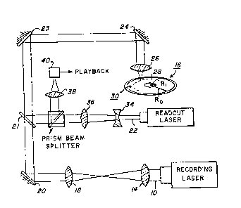
Figure 1 shows a schematic of an apparatus
for recording information on an optical recording
element 16 of the invention and for playing back the
recorded information therefrom. Referring to
figure 2, recording element 16 comprises an overcoat
layer 41, amorphous thin film optical recording
layer 42 on substrate 45. In response to a drive
signal, the intensity of a diode recording beam is
modulated in accordance with information to be
recorded on thin film 42. The modulated laser beam
is c,ollected by a lens 14 and collimated by a lens 18
and is directed by means of mirror elements 20, 23
and 24 to a lens 26 which focuses the modulated laser
beam to a recording spot 28 on the film 42 as shown
in Figure 1.
During recording, the element 16 is spun at
a constant rate, e.g. 1800 rotations per minute
(rpm~. As a result, a track of information 30 is
~.~706~
recorded on the optical recording layer in the form
of selected crystallized areas. ~s recording con-
tinues, the recording spot 28 is caused (by means not
shown3 to scan radially inward across the element 16,
5 thereby causing information to be recorded along a
spiral or concentric track that extends from an outer
radius rO to an inner radius ri. The sizes and
spacings of the recorded information marks ~ary in
accordance with the information content of the
recording laser dri~e signal, as well as with radial
position on the element 16.
During the readback process, the new
information bearing element 16 is spun at the same
rate as it was spun during the recording process.
15 laser beam 22 from a readout laser is expanded in
diameter by means of lenses 34 and 36. The optical
path of the readout lasar beam is folded by a beam
splitter 21 and mirrors 23 and 24 so that the readout
laser beam is focused to a playback spot on the
20 element 16 by the high numerical aperture lens 26.
The element 16 is assumed to be of the reflecti~e
type so that the radiation forming the playback spot
is reflected back through the high numerical aperture
lens 26 after interacting with the information marks
25 recorded on the optical element 16. ~ lens 38
directs reflected laser racliation which has been
di~erted by the prism beamsplitter onto a detector 40
which produces an electrical playback signal in
response to temporal ~ariations (contrast) in the
30 irradiance of the reflected laser radiation falling
on the detector.
The amorphous thin film optical recording
layers of this inuention are written upon with a
coherent beam of electromagnetic radiation of suffi-
35 cient energy to con~ert selected portions of the
~'~70640
amorphous film 42 to a crystalline state. In thepresent inuention the amorphous thin film optical
recording layers are of sufficient sensitiuity that
laser powers o~ about 2 to 10 mW at laser pulsewidth
5 of 40 to 100 nanoseconds prouides sufficient energy
to make the conuersion.
Recordings on the amorphous thin film were
made with a static pit tester.
The static pit tester prouides automated
10 facilities in which a microcomputer controls the
sample position, the laser power and the laser pulse
width. Each recording layer is exposed with a 830
nanometer laser diode in the static pit tester to
produce a matrix of spots in which the laser power is
15 uaried from 4 to 12 mW and the pulse width uaried
from 40 to 30,000 nanoseconds. The suitability of
the recording layer for optical recording is deter-
mined by measuring the change in reflection between
the exposed and unexposed areas of the sample, i.e.
20 between the crystalline and amorphous states.
This reflection change is expressed as
recording contrast, CT, by the following definition:
R - R
CT Rc + Rt~ X %
wherein Rt and Ra are the reflectances of the
crystalline and the aot)rphous states, respectiuely.
minimwm contrast of 5 percent must be achie~ed for the
films to be considered useful as optical recording
30 layers
The thin amorphous film recording layers can
be prepared by conuentional thin film deposition
techniques such as euaporation, RF (radio frequency~
and DC (direct current) sputtering from an alloy
35 target, and RF and DC co-sputtering from targets of
~ ~7064C,~
the indi~idual elements. Enhancement of sputtering
processes by applying magnetic fields (magnetron
sputtering) can also be usecl. The thickness of the
films can be from a few tens to a few hundreds nano-
5 meters depending on compromises among factors such ascontrast, sensitiuity, production rate, material cost,
ease of control, data rate, etc.
Supports which can be used include plastic
films, such as polyethylene terephthalate, polymethyl
10 methacrylate, and polycarbonate, a glass plate, paper
and metallic plates.
The practice of the in~ention is further
described in the following examples. In the examples,
each thin film optical recording layer is represented
by the symbol SbxInySnz wherein x, y and z are
atom percents.
Example 1
Two amorphous thin film optical recording
20 layers of this in~ention were prepared by a sputtering
process. ~ target composed of mixed Sb and In powders
was pre-sputtered in an 8 mtorr ~r atmosphere for one
hour. The pre-sputtering step was designed to achie~e
a steady state deposition condition.
Thin films of about 80 nm in thickness were
then prepared by sputtering the pre-sputtered mix for
3.5 minutes. The spwttered mix was deposited as a
thin film on a glass support. The atomic fraction of
each component in the prepared film was determined by
30 inducti~ely coupled plasma (ICP).
Figure 3 shows the amorphous to crystalline
temperature of thin films of antimony-indium compris-
ing a) 13 atom percent indium (cur~e 1) and b) 18 atom
percent indium. The transition temperatures were for
35 film a) (cur~e 2) 144C ancl for film b) 175C. The
1.;~7(3~4V
-lo-
heating rate was 25 milli-Kel~in per second. These
high transition temperatures show that the amorphous
state of the films are uery stable. This is an
important keeping property. Spontaneous transition
5 from amorphous to crystalline would be detrimental to
optical recording layers in that the reflectance
difference between the crystalline areas and amorphous
areas would be lost.
Figure 3 also shows the excellent contrast
10 achie~ed with the thin film antimony-indium layers of
the in~ention.
~ nother sample of the thin antimony-indium
film comprising 13 atom percent of indium was written
upon using the static pit tester described herein
15 before. The writing was in the form of crystallized
marks on the films. The fi].m (Sb~7Inl3) with the
crystallized written spots was placed in a chamber at
70C and 30 percent relati~e humidity for an acceler-
ated stability test. ~fter 45 days, the film was
20 examined. We did not obser~e any phase change or
corrosion on the unwritten area or the written spots.
The film did not ha~e any o~ercoat as a protecti~e
layer against corrosion. This test shows that the
films of the in~ention bearing written spots are
25 thermally and en~ironmentally stable.
~ nother film sample comprising 13 atom
percent indium was subjected to performance tests on
the static pit tester. ~ pulsed semiconductor laser
beam with a wauelength of 830 nm was used for
30 writing. The writing sensiti~ity and contrast at
~arious powers and pulse widths are shown in
Figure 4. Figure 4 shows the percent contrast between
the initial reflectance of the amorphous state and the
final reflectance of the crystallized state is clearly
35 measurable and can thus be read by state of the art
1~(364()
laser read systems. This data also shows a) that the
thin films can be written upon using practical laser
powers and writing speeds and b) the reflectiuity of
the crystalline state is higher than the amorphous
5 state.
Example ?
~ number of amorphous Sb-Sn and Sb-In thin
films with a range of compositions were prepare~
10 according to the method in Example 1. Some
representatiue compositions are Sb75Sn25, Sb70Sn30,
sb92In8~ Sb77In23 an~ Sb7lIn2~
can be written upon with a laser pulse length of 50 ns
ancl power of 6 mW. The last film can be written upon
15 at a laser pulse length of 1 ~s and power of 6 mW.
Example 3
Thin films of about 100 nm in thickness were
then prepared by sputtering for 3.5 minutes as in
20 example 1. Figure 5 shows the amorphous to crystal-
line temperature and reflectance of seueral different
thin films of the inuention hauing a Sb/In ratio of 5
and comprising specified atom percent Sn.
The amorphous to crystalline transition
25 temperature, the percent Sn an~ curue number is set
out below:
Curue No. Temperature O~C X Sn
36 174 20
30 37 204 10
38 206 3
41 210
39 207 1.3
208 2.3
1~70~4~3
-12-
~lso note that, in Figure 5, the contrast
increases with increasing Sn content in the films.
The reflectance of the crystalline areas were con-
sistently greater than the amorphous areas.
~nother thin film sample (Sb64In165n20) was
written upon using the static pit tester described
herein before. The writing was in the form of
crystallized marks on the films. The film with the
crystallized written spots was placed in a chamber at
10 70C and 30 percent relati~e humidity for an accel-
erated stability test. ~fter 14 days, the film was
examined. We did not obserue any phase change or
corrosion on the unwritten film or the written
spots. The film did not ha~e any o~ercoat as a
15 protectiue layer against corrosion. This test shows
that the films of the in~ention bearing written spots
are both thermally and en~ironmentally stable.
~ nother film sample (Sb64Inl6Sn20) was
subjected to performance tests on the static pit
20 tester. ~ pulsed semiconductor laser beam with a
wa~elength of 830 nm was used for writing. The
writing sensiti~ity and contrast at ~arious powers
and pulse widths are shown in Figure 6. Figure 6
shows the percent contrast between the initial
25 reflectance of the amorphous state and the final
reflectance of the crystallized state is clearly
measurable and can thus be read by state of the art
laser reacl systems. This data also shows that the
thin films can be written upon using practical laser
30 powers and writing speeds.
e 4
~ number of amorphous thin films with a
range of compositions were prepared according to the
35 method in Example 1. Some of the representati~e
1~70640
compositions were SbgoIngSnl Sb82Inl6Sn2'
Sb In Sn5, Sb75In24Sn1~ Sb74In7 19 71 23 7
Sb66In14Sn20~ 56 19 25 55 34 11
films can be written upon at a laser pulse length of
50 ns and power of 6mW.
Example 5
Seueral homogeneous Sb-In-Sn alloy sputter-
ing targets with uarious compositions were prepared
by hot-pressing. The thin films were prepared by the
10 sputterin~ process. Some
representatiue compositions are Sb80In20,
Sb In Sn , Sb70IngSn21, Sb70 30 65 15 20
62 12 26' and Sb61In15Sn24, Sb60In Sn
57 21 22' Sbs3Irl13Sn34, Sb51In Sn
51 19 30 and Sb50In10sn4o~ These films were
amorphous and can be crystallized at a laser pulse
length of 50 ns and power of 6 mW.
None of the thin film optical recording
layers in the aboue examples could be switched
20 between two different crystalline states.
r~ s
Thin film layers were prepared in which the
alloy compositions were a) Sb40In2Sn58and b)
Sb48In50Sn2. Film 1 was crystalline when
25 deposited. Film 2 was amorphous when deposited, but
extremely difficult to crystallize. 50th of these
films are outside the scope of the present inuention.
The inuention has been described in detail
with particular reference to preferred embodiments
30 thereof, but it will be understood that uariations
and modifications can be effected within the spirit
and scope of the inuention.