Une partie des informations de ce site Web a été fournie par des sources externes. Le gouvernement du Canada n'assume aucune responsabilité concernant la précision, l'actualité ou la fiabilité des informations fournies par les sources externes. Les utilisateurs qui désirent employer cette information devraient consulter directement la source des informations. Le contenu fourni par les sources externes n'est pas assujetti aux exigences sur les langues officielles, la protection des renseignements personnels et l'accessibilité.
L'apparition de différences dans le texte et l'image des Revendications et de l'Abrégé dépend du moment auquel le document est publié. Les textes des Revendications et de l'Abrégé sont affichés :
| (12) Brevet: | (11) CA 1270895 |
|---|---|
| (21) Numéro de la demande: | 1270895 |
| (54) Titre français: | PLAQUES DE DEVIATION ELECTROSTATIQUE EN SEMICONDUCTEUR AVEC COUCHE CONDUCTRICE |
| (54) Titre anglais: | CONDUCTIVE COATED SEMICONDUCTOR ELECTROSTATIC DEFLECTION PLATES |
| Statut: | Périmé et au-delà du délai pour l’annulation |
| (51) Classification internationale des brevets (CIB): |
|
|---|---|
| (72) Inventeurs : |
|
| (73) Titulaires : |
|
| (71) Demandeurs : |
|
| (74) Agent: | RAYMOND H. SAUNDERSSAUNDERS, RAYMOND H. |
| (74) Co-agent: | |
| (45) Délivré: | 1990-06-26 |
| (22) Date de dépôt: | 1986-05-22 |
| Licence disponible: | S.O. |
| Cédé au domaine public: | S.O. |
| (25) Langue des documents déposés: | Anglais |
| Traité de coopération en matière de brevets (PCT): | Non |
|---|
| (30) Données de priorité de la demande: | ||||||
|---|---|---|---|---|---|---|
|
FI9-84-059
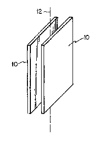
CONDUCTIVE COATED SEMICONDUCTOR
ELECTROSTATIC DEFLECTION PLATES
ABSTRACT
An electrostatic deflection plate for charged
particle beam systems is formed of a planar
semiconductive substrate having a conductive region at
the substrate surface. The conductive region is
diffused or implanted into the body of the substrate,
or one or more conductive lavers are deposited upon
the substrate surface. The substrate material is
preferably silicon and the diffused or implanted
region is formed of a nonmagnetic, nonoxidizable metal
such as gold or platinum. The deposited conductive
region may be formed of a single layer of these or
similar metals, one or more conductive underlayers
with a nonmagnetic, nonoxidizable overlayer, a single
or multilayer structure with a conductive oxide on the
outermost layer, or a metallo-organic compound which
forms a conductive layer during following heat treat-
ment. The deflection plates are fabricated using
conventional semiconductor processes and form durable
structures which minimize eddy current effects.
Note : Les revendications sont présentées dans la langue officielle dans laquelle elles ont été soumises.
Note : Les descriptions sont présentées dans la langue officielle dans laquelle elles ont été soumises.
2024-08-01 : Dans le cadre de la transition vers les Brevets de nouvelle génération (BNG), la base de données sur les brevets canadiens (BDBC) contient désormais un Historique d'événement plus détaillé, qui reproduit le Journal des événements de notre nouvelle solution interne.
Veuillez noter que les événements débutant par « Inactive : » se réfèrent à des événements qui ne sont plus utilisés dans notre nouvelle solution interne.
Pour une meilleure compréhension de l'état de la demande ou brevet qui figure sur cette page, la rubrique Mise en garde , et les descriptions de Brevet , Historique d'événement , Taxes périodiques et Historique des paiements devraient être consultées.
| Description | Date |
|---|---|
| Inactive : CIB de MCD | 2006-03-11 |
| Inactive : CIB de MCD | 2006-03-11 |
| Inactive : CIB de MCD | 2006-03-11 |
| Le délai pour l'annulation est expiré | 2001-06-26 |
| Lettre envoyée | 2000-06-27 |
| Accordé par délivrance | 1990-06-26 |
Il n'y a pas d'historique d'abandonnement
| Type de taxes | Anniversaire | Échéance | Date payée |
|---|---|---|---|
| TM (catégorie 1, 7e anniv.) - générale | 1997-06-26 | 1997-05-28 | |
| TM (catégorie 1, 8e anniv.) - générale | 1998-06-26 | 1998-05-14 | |
| TM (catégorie 1, 9e anniv.) - générale | 1999-06-28 | 1999-05-17 |
Les titulaires actuels et antérieures au dossier sont affichés en ordre alphabétique.
| Titulaires actuels au dossier |
|---|
| INTERNATIONAL BUSINESS MACHINES CORPORATION |
| Titulaires antérieures au dossier |
|---|
| DOUGLAS GRAHAM CULLUM |
| GEORGE JOSEPH GIUFFRE |
| MARIS ANDRIS STURANS |
| TIMOTHY ROBINSON GROVES |
| WERNER STICKEL |

