Note : Les descriptions sont présentées dans la langue officielle dans laquelle elles ont été soumises.
~X71~30~3
POWER CONVERSION SYSTEM
BACKGROUND OF THE INVENTION
Field of the Invention
________________ __
The present invention relates to a power conversion
system including a plurality of conversion units having
substantially the same structure and operating in parallel
to suppl~ a.c. power to a common load.
The background of the invention as explained below
makes reference to Figures 4 and 5 of the accompanying
drawings. For the sake of convenience, all of the
drawings will first be introduced briefly, as follows:
Fig. 1 is a block diagram showing the inventive power
converter system including two inverter units;
Fig. 2a is an equivalent circuit of the main circuit
in the power converter system shown in Fig. l;
Fig. 2b is an equivalent circuit of the simulation bus
circuit of Fig. l;
Fig. 3 ifi a schematic diagram showing in part another
embodiment of the present invention;
Fig. 4 is a block diagram showing the conventional
power conversion system of the prior art; and
Fig. 5 is a waveform diagram showing the signals
observed in synchronized rectification circuit used for
detection of ~P and ~Q signals.
Descri~tion of the Prior Art
______ __________________ _
Fig. 4 shows a conventional inverter system of the
prior art disclosed in Japanese Publi~hed Patent
Appllcations Nos. 53-36137 and 56-13101. In the figure,
7~80~3
- la -
#1 and #2 inverter units 1 and 2 having the same construc-
tion are operated in parallel to supply power through an
output bus 3 to a load 4.
The inverter unit 1 comprises an inverter circuit 100,
an output transformer 101, and a reactor 102 and a capaci-
tor 103 constituting a filter. The inverter unit 1
converts power supplied from a d.c. power source 5 into
a.c. pow~r, which i8 conducted through an output switch
104 to the output bus 3.
Next, the operation of the above inverter system will
be de~cribed. When the parallel operation of the two
inverter units 1 and 2 is necessary, the output current
Il of the ~1 inverter unit 1 is detected as a signal
Ila by a current transformer (CT) 106, and in the same
way the output current of the #2 inverter unit 2 is
1271~'08
detected as a signal I2a. A lateral current detector 107
provided in the inverter unit 1 evaluates the difference
between Ila and I2a to produce a signal ~I representing
a lateral current flowing between the units. A phase
shifter 108 produces two perpendicularly-intersecting
voltage vectors EA and EB, and arithmetic circuits 109
and 110 evaluate the reactive power component ~Q and
effective power component ~P based on the detected signal
~I and the respective voltage vectors EA and EB. Based
on the siynals provided by a voltage setting circuit 111
and voltage feedback circuit 112, a voltage control
circuit 113 operates on a pulse width modulation (PWM)
circuit 114 to implement pulse width modulation for the
inverter circuit 100, thereby controlling the output
voltage.
The above-mentioned reactive power component ~Q is
given to the voltage control circuit 113 as a supple-
mentary signal, so that the reactive power component ~Q
is nulli~ied by regulating the inverter output voltage
within a few percent range. The effective power
component value ~P is fed through an amplifier 115
constituting a PLL circuit to a reference oscillator 105
so that its output frequency is adjusted finely, thereby
controlling the phase of inverter output voltage to
nullify the effective power component ~P.
By controlling the inverter output voltage and
phase so as to nullify both of the reactive and effective
~L2';~30~3
power components ~Q and ~P, no lateral current f lows
between the two inverter units and the load is shared
stably by the units.
The conventional inverter system employing the
parallel operation system as described above, needs a
test as to whether it operates normally as expected, and
the only test method is to operate the system by
connecting the first and second inverter units 1 and 2
to the output bus 3 in Fig. 4. However, as is known in
the art, the usual inverter have an overcurrent
withstanding capability of only 150% of the rated current
in general, and therefore it is extremely difficult to
test the control circuit and adjust the response of
control while actually operating the system of Fig. 4.
In practice, individual components of the control
circuit shown in Fig. 4 are tested and adjusted
completely and wiring between the components is checked
before conducting the running test for the overall
~ystem shown in Fig. 4. Even with such a prudent
procedure for the parallel operation, it frequently
occurs that an unexpected fault causes an excessive
lateral current and the inverter fails to commutate,
resulting in a damage to the system. This implies
difficulties in investigating a fault (particularly an
intermittent fault such as that caused by a faulty
electric contact) and also in conducting a periodical
maintenance service.
~71808
In a control unstability caused by an unexpected
harmonic lateral current included in the output current
Il of each inverter unit, harmonic current in large
proportions included in the detected lateral current
signal ~I disturbs the detection of the intersecting
current components, causing the unstability. In this
case, the output filter capacitor 103 provided for each
inverter unit forms a resonance circuit in conjunction
with other capacitors of other inverter units through
the inductance of output bus 3. The resonance frequen-
cies, which depend on the length of wiring, are in many
cases relatively high above the seventh harmonic.
Harmonics created by any of the parallel-connected
inverter units resonate in this resonance circuit,
yielding a very large harmonic lateral current. In the
case of synchronized rectifying circuits used as the
arithmetic circuits 109 and 110, the harmonic lateral
current produces the following signals. Fig. 5 (b) and
(c) shows the signals ~P and ~Q derived from a
fundamental lateral current signal ~I shown in Fig. 5(a)
throuqh the synchronized rectification. Assuming a case
that the signal ~I is not of the fundamental component,
but a ~I of the fifth harmonic component exists as a
harmonic lateral current as shown by (d) in Fig. 5.
Synchronized rectification for this signal yields a ~P
component signal shown by (e) and a ~Q component signal
shown by (f) in Fig. 5. The ~Q signal averages out to
-- 4 --
i.~71~308
zero, while the ~P signal remains in its positive parts
as shown by hatching. A positive ~P signal indicates an
excessive share of effective power by the associated
inverter unit, causing the PLL amplifier 115 to lower
temporarily the oscillation frequency so as to produce a
lag phase of the inverter unit 1. The harmonic lateral
current shown at (d) in Fig. 5 has an opposite phase for
the inverter unlt 2, causing its ~P signal to be negative,
and the amplifier 115 in the inverter unit 2 operate to
lead the phase of the inverter unit 2. In actual,
however, there is no la-teral current of fundamental
component between the inverter units 1 and 2, requiring
no adjustment for the phase difference, and the above-
mentioned PLL circuit operation in response to the ~P
signal i5 erroneous, resulting in an increased lateral
current of the fundamental component and eventually in
the unstability of parallel operation. Althoug}l in the
examplary case shown by (d), (e) and (f) in Fig. 5 the
fi~th harmonic wave has a phase relationship with the
fundamental wave as shown, but in actual case various
phase relationship occurs, so both the ~P and ~Q signals
will have various values in even positive and negative.
Therefore, unstability arise not only in the phase
control, but also in the voltage control due to an
erxoneous ~Q signal. Although the example of Fig. 5
deals with the fifth harmonic wave for the sake of
simplicity, it will be apparent that abnormal ~P and ~Q
-- 5 --
~;~71~08
signals can equally result generally for the nth harmonic
wave. In general, the nth harmonic wave e~erts an
influence of l/n gain on the system as a result of
synchronized rectification, disturbing the control system
of a parallel operating inverter system as shown in
Fig. 4.
In order to overcome the foregoing problems, there
is known a method of multiplication between the signal ~I
and sinusoidal EA and EB signals using multipliers as
arithmetic circuits 109 and 110. However, multipliers
are generally complex in construction, and therefore
relatively susceptible to failure, and expensive. On
this account, it is much desirable for the system as
shown in Fig. 4 to employ simpler and more reliable
synchronized rectification circuits.
SUMM7~RY OF THE INVENTION
It is an object of the present invention to provide
a parallel-operating power conversion system which allows
testing and adjustment of parallel operation control
without actually operating the main circuits in parallel,
but merely using the control circuit, and also allows
stable load sharing in parallel operation even if a
harmonic lateral current flows between the main circuits.
The inventive system includes a plurality of
converter units each including a main circuit which has
its converter circuit connected to a load bus and
further including a simulation bus circuit connected
r
-- 6 --
1 ~ 71 8~
through a simulation bus to counterparts of all remaining
converter units. The output voltage and frequency of the
converter circuit are controlled basing on the reactive
and effective power detected on the simulated bus
circuits. Since the simulation bus circuit of one
converter unit is connected with the simulation bus
circuits of other converter units, the output voltage
and frequency of one converter circuit can be made
consistent, prior to its connection to the bus, with the
output of other conversion units already connected to
the bus.
In one aspect of the present invention, the power
conversion system comprises a plurality of converter
units having their output terminals connected through a
common bus to a load. Each converter unit includes a
circuit for converting a d.c. or a.c. input power into
an a.c. power of an intended voltage and frequency, an
impedance element connected through a switch between the
output terminal of the converter circuit and the bus, a
simulation bus circuit including an impedance element
connected to the output terminal of at least one converter
pole of the converter circuit, and a means for controlling
the output voltage and frequency of the converter circuit
on the basis of the current on the simulation bus
circuit, with one end of the simulation bus circuit
being connected through the simulation bus with one end
of other simulation bus circuit of all remaining
converter units.
- 7 -
~'~71~08
The conversion circuit is typically a voltage type
or current type inverter, but it may be a converter of
any type such as a cycloconverter. The present invention
can also be applied to a rectangular wave output inverter
of variable frequency and variable voltage. The
converter circuit of each converter unit may be same or
may be different.
DETAILED DESCRIPTION OF T~IE PREFERRED EMBODIMENTS
In Fig. 1 is illustrated an inverter system
embodying this invention including two inverter units 1
and 2. The inverter units 1 and 2 have substantially the
same structure, and the following description on unit 1
i5 applicable also to unit 2. The first inverter unit 1
~'~71808
comprises an inverter circuit 100, an output transformer
101, a reactor 102 and capacitor 103 constituting a
filter in combination, an output switch 104, a reference
oscillator 105, a phase shifter 108, arithmetic circuits
109 and 110, a voltage setting circuit 111, a voltage
feedback circuit 112, a voltage control circuit 113, a
PWM circuit 114, and a PLL amplifier 115. These system
elements are substantially identical to those used in the
conventional inverter unit as described previously in
connection with Fig. 4 and detailed explanation thereof
will be omitted here. The inverter units 1 and 2 can
supply their a.c. outputs through the output switches to
a load 4 on the common bus, as in the arrangement of
Pig. 4.
In this inverter system, the inverter unit 1 has a
transformer 120 connected to the output of the inverter
- circuit 100, with its secondary winding being connected
to a simulation bus 7 through a reactor 121 serving as a
simulation bus circuit, a current transformer 123 and a
switch 122. The phase shifter 108 has its input terminal
connected through the reactor 121 to the secondary
winding of the insulation transformer 120. As an another
modification the phase shifter can be connected to the
capacitor 103. The transformer 120 may be of a small one
having a power capacity of less than 1 kVA for the
inverter 100 having a power capacity of more than 100 kVA.
The secondary voltage of the transformer 120 can be
chosen arbitrarily, e.g., 100 volts.
_ 9 _
" ~71808
Next, the operation of the inverter unit 1 will be
described. Assuming the current rating of the reactor
121 to be 1 ampere in correspondence to the rated current
of the inverter circuit 100 and further assuming the
composite impedance of the main reactor 102 and
transformer 101 to be 10 percent, the composite impedance
of the reactor 121 and transformer 120 is set to lOQ.
Similarly, both combinations preferably have impedance
angles selected as near as possible.
By setting the circuit parameters as mentioned above,
the circuit connected to the simulation bus 7 constitutes
a model of the parallel-operating main circuit excluding
the ~ilter capacitor and load in Fig. 1. Namely, the
main circuit has a complete equivalent circuit shown in
Fig. 2a, while the above-mentioned model is expressed as
shown in Fig. 2b. The current Il in Fig. 2a includes
both the lateral current and the load current, whereas
the current in Fig. 2b is solely the lateral current, and
therefore a current Ilo in Fig. 1 representing the
lateral current ~I can be obtained without the use of the
lateral current detecting circuit 107 shown in Fig. 4.
Accordingly, through the lA/O.lA conversion, for example,
by the current transformer (CT) 123 to produce the
lateral current signal ~I, the same control operation as
described in connection with Fig. 4 can be executed.
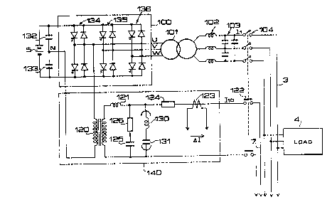
Fig. 3 shows another embodiment of this invention,
in which the same portions as those of Fig. 1 are
-- 10 --
~718(~8
omitted for the sake of simplicity, but the lateral
current evaluating circuit is shown in detail. The
components having the same functions as those of Fig. l
are referred to by the common symbols and explanation
thereof is omitted.
In the figure, the power conversion system comprises
a transformer 120 having a primary winding connected
between the neutral point N of the d.c. power source at
the node of serial-connected capacitors 132 and 133 and
phase U representing the three-phase output of inverter
poles 134, 135 and 136. For the enhanced analogy to the
main circuit, the transformer secondary circuit is
provided with a capacitor 125 in correspondence to the
filter capacitor 103 in serial connection with a damping
resistor 126 which prevents resonance of the capacitor
125 with the counterpart in the second inverter unit 2.
The damping resistor 126 may also be arranged in series
to the switch 122 as shown by resistor 124 in the figure.
The transformer secondary circuit may further be provided
with a combination of a reactor 130 and capacitor 131
serving as a resonance filter which does not exist in the
main circuit, so that harmonic components are eliminated
thoroughly thereby to produce the control signal immune
to the harmonic currents.
The arrangement shown in Fig. 3 has a primary
feature that the control circuit can be tested and
adjusted through the simulated bus preparatory to the
~71808
parallel operation without closing the output switch 104,
but merely closing the switch 122, whereby testing,
adjustment and inspection of the system are carried out
easily.
The second feature is that the operating signal can
be detected without any influence of a harmonic lateral
current flowing between the main filter capacitors 103 of
inverter units, whereby a stable control system can be
designed easily.
In the above embodiment, the inverter main circuit
is for three-phase, while the simulated bus circuit
composed by transformer 120, reactor 121, capacitor 125,
resistor 126 and etc. is for single-phase. This is
based on that the inverter usually controls for three
f 15 phases in the lump, and therefore load sharing control
is required only for a representing phase. Obviously,
much high-response load balancing can be performed by
provision of the circuit shown in Fig. 3 for each of
three phases.
Although the above described is devoted to a
voltage-type inverter of a constant voltage, constant
frequency and sinusoidal output waveform, the present
invention can equally be applied to any power conversion
systems of types such as current-type inverters and
cycloconverters. The invention can also be applied to
variable-frequency, variable-voltage inverters producing
a switched output waveform, and to the arrange~ent
including converter units of different power capacities.
- 12 -
1~718()8
According to the present invention as described
above, the parallel operation control circuit can be
tested and adjusted without actually connecting the main
circuits in parallel, and also by using a synchronized
rectification control circuit which does not use
multipliers, stable control system which is immune to a
harmonic lateral current between the main circuits can
be designed, whereby a reliable and inexpensive control
circuit can be realized.
- 13 -