Note : Les descriptions sont présentées dans la langue officielle dans laquelle elles ont été soumises.
SPECIFICATION
TITLE OF THE INVENTION
SIGNAL CONVERTER
BACKGROUND OF THE INVENTION
Field of the Invention
.
The present invention relates to a signal
converter used in a tuning device for a radio receiver,
a television receiver and the like.
Prior Art
Ferromagnetic resonator, for example, YIG (YIG
in the specification including yttrium iron garnet
together with various additives) resonator using YIG as
ferromagnetic resonance element, is advantageous in that
Q of resonance characteristics is high at microwave
band, compact constitution is possible because the
resonance frequency is not varied by the volume of the
YIG element, and the resonance frequency can be varied
linearly in wide band region by varying the bias
magnetic field applied to the element. Consequently, in
recent years, in a receiver of high frequency signal
such as microwave, a magnetic resonance element of YIG
-- 2 --
, 1~,
~ ~ 7~
monocrystalline sphere or YIG monocrystalline sphere has
been used as a resonance circuit for a tuning circuit.
Such constitution is proposed in Japanese unexamined
patent applications laid-open No. 137609/1975, No.
78201/1975, No. 60402/1974 and No. 71215/1975.
When a signal converter for tuning circuit is
composed of a filter circuit and a local oscillator
using YIG resonator, the filter circuit and the local
oscillator must be coincident in the resonance
characteristics. If the YIG monocrystalline sphere or
plate is used, however, it cannot be manufactured
uniformly and precisely in the shape and size and
dispersion is apt to occur in its characteristics.
Consequently, the resonance characteristics are not
coincident between the filter circuit and the local
oscillator thereby tracking error may occur. In order
to correct such error, a special circuit constitution as
disklosed in the patent application laid-open No.
137609/1975 is required thus the whole circuit
constitution becomes complicated.
OBJECT AND SUMMARY OF THE INVENTION
It is an object of the present invention to
- provide an improved signal converter using ferromagnetic
1~ 7
resonance.
It is another object of the present invention
to provide an improved signal converter useful in tuning
device.
It is further object of the present invention
to provide a signal converter having a simple
construction and suitable for making in a small size.
It is still further object of the present
invention to provide a signal converter improved in
temperature stability.
According to one aspect of the present
invention there is provided a signal converter which
comprises a filter formed of a first ferromagnetic
resonator supplied with an input signal to be converted
and deriving a filtered signal having a first frequency,
a local oscillator formed of an active element and a
second ferromagnetic resonator connected to said active
element, deriving an oscillating signal having a second
frequency, a mixer mixing said filtered signal and said
oscillating signal and deriving a converted signal, said
first ferromagnetic resonator being formed of a first
ferrimagnetic crystal, a microstrip line magnetically
coupled to said ferrimagnetic crystal and first D.C.
bias magnetic field means applying a first D .C . bias
12 71 ~
magnetic field to said first ferrimagnetic crystal, said
second ferromagnetic resonator being formed of a second
ferrimagnetic crystal, a microstrip line magnetically
coupled to said second ferrimagnetic crystal, and second
D.C. bias magnetic field means applying a second D.C.
hias magnetic field to said second ferrimagnetic
crystal, said first and second ferrimagnetic crystal
being composed of ferrimagnetic thin films formed by a
thin film forming technique.
According to another aspect of the present
invention there is provided a signal converter
comprising a first local oscillator formed of a first
active element and a first ferromagnetic resonator
connected to said first active element, deriving a first
oscillating signal having a firs~ frequency, a first
mixer mixing said first oscillating signal and an input
signal to be converted and deriving a mixed signal, a
filter formed of a second ferromagnetic resonator
supplied with said mixed signal and deriving a filtered
signal having a second frequency, a second local
oscillator formed of a second active element and a third
ferromagnetic resonator connected to said second active
element and deriving a second oscillating signal having
a third frequency, a second mixer mixing said filtered
~;~7~8~ ;~
signal and said second oscillating signal and deriving a
converted signal, said first ferromagnetic resonator
being formed of a first ferrimagnetic crystal, a
microstrip line magnetically coupled to said
ferrimagnetic crystal and first D.C. bias magnetic field
means applying a first D.C. bias magnetic field to said
first ferrimagnetic crystal, said second ferromagnetic
resonator being formed of a second ferrimagnetic
crystal, a microstrip line magnetically coupled to said
second ferrimagnetic crystal and second D.C. bias
magnetic field means applying a second D.C. bias
magnetic field to said second ferrimagnetic crysta],
said third ferromagnetic resonator being formed of a
third ferrimagnetic crystal, a microstrip line
magnetically coupled to said third ferrimagnetic crystal
and third D.C. bias magnetic field means applying a
third D.C. bias magnetic field to said third
ferrimagnetic crystal, said first, second, and third
ferrimagnetic crystal being composed of ferrimagnetic
thin films formed by a thin film forming technique.
BRIEF DESCRIPTION OF THE DRAWINGS:
Fig. 1 is a block diagram of a receiver as an
embodiment of the invention;
~i~718~X
Fig. 2 is a plan view of YIG filter;
Fig. 3 is a sectional view taken in line A-A
of Fig. 2;
Fig. 4 is a plan view of a local oscillator;
Fig. 5 is a sectional ~iew taken in line A-A
o Fig. 4;
Fig. 6a and 6b is a block diagram of an
oscillator;
Fig. 7 is a diagram of circuit constitution of
the oscillator;
Fig. 8 is Smith chart illustrating oscillation
action;
Fig. 9 is a plan view of a receiver as an
example;
Fig. 10 is a sectional view taken in line A-A
of Fig. 9;
Fig. 11 through Fig. 13 are sectional views of
magnetic field applying means;
Fig. 14 is a graph illustrating magnetostatic
mode generated in a circular ferrimagnetic thin film;
Fig. 15 is a graph illustrating distribution
of internal d.c. magnetic field of the circular
ferrimagnetic thin film;
Fig. 16 is a graph illustrating relation
~27~8~2
between distribution of the internal d.c. magnetic field
and the magnetostatic mode in the circular ferrimagnetic
thin film;
Fig. 17 is a perspective view of a magnetic
resonance element;
Fig. 18 is a sectional view of the magnetic
resonance element;
Fig. 19 is a graph illustrating insertion loss
in the magnetic resonance element;
Fig. 20 is a graph illustrating insertion loss
in a comparison example;
~ Figs. 21 and 22 are graphs illustrating
distribution of demagnetizing field in the circular
ferrimagnetic thin filmi
Fig. 23 is a perspective view of a magnetic
resonance elemen~;
Fig. 2~ is a graph illustrating insertion loss
of the magnetic resonance element;
Fig. 25 is a diagram illustrating schematic
constitution of a magnetic circuit;
Fig. 26, Fig. 27 and Fig. 30 are diagrams
illustrating schematic constitution of magnetic circuits
to be applied to the invention;
Fig. 28 and Fig. 29 are diagrams illustrating
-- 8 --
1~71~1~
relation between the magnetic adjuster and temperature
variation of the resonance frequency;
Fig. 31 and Fig. 32 are diagrams illustrating
characteristics of a magnetic circuit; and
Fig. 33 and Fig. 34 are block diagrams of
receivers as other embodiments of the invention.
DESCRIPTION OF THE PREFERRED EMBODIMENTS
A signal converter as an embodiment of the
invention will now be described referring to Fig. l.
The embodiment is of superhetorodyne type, and comprises
an antenna 1, a high-frequency filter circuit 2 using
ferromagnetic resonator such as YIG resonator, a high-
frequency amplifier 3, a mixer 4, a local oscillator 5
including a resonator using ferromagnetic resonator such
as YIG resonator, and magnetic field applying means 6
and 7 which supply magnetic fields variably to YIG
resonator elements in the filter circuit 2 and the local
oscillator 5 respectively. Both means 6 and 7 may be
adjusted in interlocking. Resonance frequency of the
YIG element in the filter circuit 2 is adjusted by the
means 6, thereby selection of pass band center frequency
in the filter circuit 2, that is, selection of tuning
frequency or tuning action is effected. In this case,
~7:18~12
signal received from the antenna 1 is introduced to the
YIG filter circuit 2, and signal of frequency fs passing
through the filter circuit 2 is amplified by the high-
frequency amplifier 3 and then introduced to the mixer 4
and mixed with local oscillation signal of frequency fL
from the local oscillator 5, and signal of intermediate
frequency fS-fL is taken out from the mixer 4.
In the invention, special constitution is
adopted in the YIG filter circuit 2 and the YIG
resonator of the local oscillator 5.
The magnetic resonance element is formed on a
common paramagnetic substrate such as GGG
(gadolinium-gallium-garnet) substrate by means of thin
film forming method, such as sputtering, chemical vapor
deposition (CVD) or liquid phase epitaxy (LPE), into a
ferrimagnetic thin film, e.g. YIG thin film. The YIG
thin film is patterned by photolithography thereby both
YIG thin film magnetic resonance elements are
simultaneously formed on the common GGG substrate. In
this case YIG thin film elements to constitute the YIG
filter circuit 2 and the YIG resonator of the local
oscillator 5 respectively have the same ~hape, such as
disk, square or rectangular shape. Difference of
resonance frequencies, that is, offset frequency can be
-- 10 --
12718~
set by selecting aspect ratio of each YIG thin film
element, for example, ratio of film thickness to
diameter in the case of disk shape. If both YIG thin
film elements are formed by the same film, in the case
of disk shape, offset frequency is set by selecting
different diameters of both elements. For example, if
saturated magnetization 4~Ms Of YIG is 4~Ms=1780 Gauss
and the film thickness t is 20 ~m and diameters are
selected to 4mm and 2mm respectively, aspect ratio
becomes 0.005 and 0.01 and the offset frequency becomes
56MHz. Both elements are disposed in the same magnetic
field. For example, both magnetic field generating
means 6 and 7 in Fig. 1 may be formed commonly. Or both
elements may be selected to the same shape and size
hence the same aspect ratio and one element may be
supplied with magnetic field being different from that
of other element by a definite amount so as to set a
required offset frequency.
Both resonance elements of YIG thin film are
provided by the same thin film element in the above
embodiment. When the YIG thin film is formed on the
substrate by means of thin film forming method such as
CVD, LPE or sputtering, the film thickness can be
obtained uniformly and precisely. Consequently, even
~ ;~7~81
when both YIG thin film resonance elements are formed on
separate substrates by the same or different process,
the resonance frequency can be set accurately without
dispersion in comparison to the case where YIG
monocrystalline substance such as YIG sphere or YIG
monocrystalline plate is machined by cutting or
polishing so as to obtain YIG magnetic resonance
element.
An example of independent constitution of a
filter circuit 2 and a local oscillator 5 will be
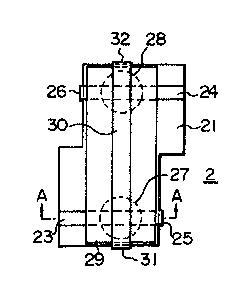
described. Fig. 2 shows a plan view of an example of
structure of the filter circuit 2 r and Fig. 3 shows a
sectional view thereof. In this example, a first major
surface of a dielectric substrate 21 of alumina or the
like has a ground conductor 22 adhered thereon, and a
second major surface has first and second micro strip
lines in parallel to each other, i.e. input and output
transmission lines 23 and 24 adhered thereon. Ends of
both strip lines 23 and 24 are connected to the ground
conductor 22 through first and second connecting
conductors 25 and 26 respectively. First and second YIG
thin film magnetic resonance elements 27 and 28 are
disposed on the second major surface of the substrate 21
in electromagnetic coupling with the first and second
- 12 -
micro strip lines 23 and 24 respectively. The first and
second magnetic resonance elements 27 and 28 are
constituted in a process that YIG thin film is formed on
a major surface of GGG substrate 29 by the thin film
forming method and then patterned in disk shape by using
photolithography technique including selective etching.
A third micro strip line, i.e. coupling transmission
line 30 is formed between the first and second magnetic
resonance elements 27 and 28 on the substrate 29 so as
to couple these element electromagnetically and adhered
to other surface of the substrate 29. Both ends of the
third strip line 30 are connected to the ground
conductor 22 through connecting conductors 31 and 32
respectively. Distance between both elements 27 and 28
is selected to ~/4 wherein ~ is wave length of the
center frequency in the pass band so that insertion loss
in the cutoff region outside the pass band is sharply
increased.
On the other hand, Fig. 4 shows an example of
structure of the local oscillator 5, and Fig. 5 shows a
sectional view taken on line A-A of Fig. 4. A first
major surface of a dielectric substrate 51 of alumina or
the like has a ground conductor 52 adhered thereon, and
a second major surface has a micro strip line 53 adhered
127183 ~
thereon. One end of the micro strip line 53 is
connected to the ground conductor 52 through a
connecting conductor 54. YIG thin film magnetic
resonance element 55 is electromagnetically coupled to
the micro strip line 53. The YIG thin film magnetic
resonance element 55 is in a process that YIG thin film
is formed on a major surface of GGG substrate 56 by the
thin film forming method and then patterned in disk
shape ~y photolithography. Numeral 57 designates a
high-frequency bipolar transistor, numeral 58 an
impedance converter, and numeral 59 a MOS capacitor for
,blocking D.C. component. In this example, base B of the
transistor 57 is connected through a wire 61 to a ground
pad 60 in turn connected to the ground conductor 52,
emitter E is connected to side of the element 55, and
collector C is connected to side of the impedance
converter 58, thereby series feedback type oscillator
utilizing common base transister is constituted.
Next, oscillation principle and condition for
the oscillation will be described in connection with the
circuit using the magnetic resonance element as a
resonator. The resonator, i.e. YIG magnetic resonance
element 55 is inserted to feedback circuit other than
output circuit. Fig. 6a and Fig. 6b are block diagrams
~ 7~ 8~
of the oscillating circuit. Numeral 62 designates YIG
resonance circuit, numeral 63 a negative resistance
circuit, numeral 64 an impedance matching circuit, and
numeral 65 a load. Numeral 66 in Fig. 6-b designates a
load impedance including the impedance matching circuit.
In Fig. 6, reflection coefficient ry at a side
of YIG resonance circuit viewing from terminal A, i.e.
side of YIG feedback circuit, and reflection coefficient
rN at a side of active element, i.e. side of negative
resistance circuit, are expressed by following formulae
using respective impedances Zy and,ZN viewing from the
terminal A.
ry= ZY -
Zy + Zo
r N = - N O ( 2)
Z N + Z O
wherein Zo: characteristic impedance (5~).
Condition of steady oscillation is expressed
by following formula using ry and rN.
r y r N = 1 (3)
- 15 -
1~:7181~
Since both ry and rN are complex numbers,
formula (3) by separating in amplitude and phase becomes
as follows:
Ir Yl I r N I e j ( ~ Y + ~ N ) = 1
hence
¦ r y ¦ ¦ r Nl = 1 (4)
~ Y + ~ N = (5)
Since the YIG feedback circuit being passive
element circuit has positive real resistance of loss
component of the YIG resonator, it follows from formula
(1) that¦ ry I < 1. Consequently, in order to satisfy
the oscillation condition of formula (4), condition
¦ ry ¦ ~ is required and it follows from formula (2)
that Zn must have negative real resistance.
The negative feedback circuit in Fig. 6 may be
a two-terminal active element of negative resistance or
a circuit composed of three-terminal active element and
feedback element. The example described in Fig. 4 and
Fig. 5 uses high-frequency bipolar transistor. Fig. 7
- 16 -
1;~718~
shows constitution of a series feedback type oscillating
circuit utilizing common base transistor, and X
designates a reactive circuit.
Above description of the oscillating circuit
relates to steady oscillation. In order that the
oscillation rises, however, following condition must be
satisfied.
¦ r Y¦ I r NSl > 1 (6)
hence
I r y I ~ Ir ~5l (7)
Wherein rNs is value of rN at small signal. If the
oscillation rises and the active element performs large
amplitude operation, absolute value of the negative
resistance decreases and value 1/¦ r Nl gradually
increases and the oscillation becomes steady when
formula (2) is satisfied.
Based on above conditions, operation principle
of the YIG oscillating circuit will be described
referring to Smith chart in Fig. 8. At small signal
state, value 1/rN is at C state in relatively inner side
~ ~ 71 8~
of ~he Smith chart. However, as the active element
performs large amplitude operation, l/rN passes through
D state and is transferred in arrow direction.
In constitution of Fig. 4 and Fig. 5, if the
YIG element 55 is not in resonance, the YIG oscillating
circuit becomes only strip line with front end
shortcircuited and therefore ry follows locus shown by A
in Fig. 8. As clearly seen from Fig. 8, since phase
condition of oscillation shown by formula (5) is not
satisfied by rN Of any amplitude, oscillation does not
occur.
If the YIG element 55 resonates at frequency
fo between fl and f2 by application of d.c. magnetic
field, y follows locus shown by B in Fig. 8 at
frequency near fo. Then, at frequency near fo,
amplitude condition of formula (7) for oscillation to
rise and phase condition of formula (5) are satisfied
simultaneously. If the oscillation rises and l/rN is
transferred from C state to D state, since formulae (4)
and (5) are simultaneously satisfied at frequency fo,
steady oscillation is effected at the oscillation
frequency fo.
Based on such principle, if d.c. applied
magnetic field is varied and resonance frequency of the
- 18 -
1;~7~83 2
YIG element is varied between fl and f2, the oscillating
circuit oscillates in tuning to frequency near the
resonance frequency.
In an example of Figs. 2 and 3 and an example
of Figs. 4 and 5, the filter circuit 2 and the local
oscillator S are formed on the separate substrates 21
and 51. However, the signal converter as a whole may be
formed integrally on a single substrate. An example of
such constitution is shown in Fig. 9 and Fig. 10. Fig.
9 is a plan view of a signal converter, and Fig. 10 is a
sectional view taken on line A-A of Fig. 9. Parts in
Fig. 9 and Fig. 10 corresponding to Fig. l through Fig.
5 are designated by the same reference numerals, and the
repeated description shall be omitted. In this case,
the above-mentioned substrates 21 and 51 are replaced by
a common substrate 91 made of alumina for example. One
major surface of the common substrate 91 has a filter
circuit 2, an amplifier 3, a mixer 4 and a local
oscillator 5 formed thereon, and other major surface has
a common ground conductor 92 adhered thereon in place of
the ground conductors 22 and 52. The GGG substrates 29
and 56 are replaced by a common GGG substrate 93, and
YIG thin film elements 27, 28 and 55 are formed on the
substrate 93. In a notch 94 provided on the substrate
-- 19 --
~ 71 81~
91, ends of micro strip lines 23, 24 and 53 are
connected to the ground conductor 92 through connecting
conductors 25, 32 and 54 respectively.
The GGG substrate may be provided with
recesses corresponding to shape and size of various YIG
thin film elements, and the YIG thin film elements may
be disposed in respective recesses.
Although magnetic field may be applied to the
YIG thin film magnetic resonance elements 27, 28 and 55
of the filter circuit 2 and the local oscillator 5 by
respective magnetic field applying means 6 and 7 as
above described, the means 6 and 7 may be constituted
commonly. For example, a yoke 81 of magnetic substance
such as permalloy is installed as shown in Fig. 11, and
in a magnetic gap 82 of the yoke 81 is disposed a
substrate 91 on which the signal converter circuit as
described in Fig. 9 and Fig. 10 is assembled. A coil 85
is wound on at least one of opposite magnetic poles 83
and 84 to constitute the magnetic gap 82 of the yoke 81,
and the magnetic field applying means 6 and 7 are
constituted commonly. Thus, the common magnetic field
is applied to the YIG thin film elements 27, 28 and 55
of the filter circuit 2 and the local oscillator 5.
This constitution can be applied to the case where the
- 20 -
1 ~ 71 8~
offset frequency is obtained by varying the aspect ratio
in the YIG elements 27, 28 and 55. When different
magnetic fields are applied to the YIG elements 27, 28
and 55 so as to obtain the offset frequency, as shown in
Fig. 12 and Fig. 13, a permanent magnet 86 is locally
arranged on at least one of the magnetic poles 83 and
84, or an auxiliary coil 87 is arranged there. Magnetic
field from the magnet 86 or the coil 87 is superposed on
magnetic field from the coil 85 in forward direction or
reverse direction so that in the magnetic gap 82 the
magnetic field intensity at the installation position of
the magnet 86 or the coil 87 is different from that at
other position by a prescribed amount, and the YIG
elements 27, 28 of the filter circuit and the YIG
element 55 of the local oscillator are arranged at
positions different in the magnetic field intensity.
When the offset frequency is varied thereby
the intermediate frequency to be taken out from the
mixer 4 is varied as in a receiver used in amateur radio
communication, current flowing through the auxiliary
coil 87 for example may be adjusted so as to adjust
difference between magnetic fields applied to respective
YIG elements of the filter circuit and the local
oscillator.
- 21 -
1;~718~2
In the invention as above described, each
resonator of the filter circuit 2 and the local
oscillator 4 is constituted by a thin film element
produced in thin film forming method to a magnetic
resonance element. Suppression of spurious response
(magnetostatic mode) is required in this case. The
magnetic resonance element by monocrystalline spheretYIG
monocrystalline sphere~ is advantageous in that
magnetostatic mode is not easily excited thereby single
resonance mode of uniform precessional mode is obtained.
However, even if the YIG thin film is located in the
high'frequency magnetic field of good uniformity, since
the internal d.c. magnetic field is not uniform,
magnetostatic mode may be much excited. Magnetostatic
mode when d.c. magnetic field is applied perpendicularly
to surface of a ferrimagnetic specimen of disk shape is
analyzed in the reference (Journal of Applied Physics,
vol. 48, July 1977, pp. 3001 - 3007), and each mode is
expressed by (n, N)m~ Wherein mode (n, N)m is a mode
having n nodes in the circumferential direction, N nodes
in the diameter direction, and ~m-l) nodes in the
thickness direction. If the high-frequency magnetic
field has good uniformity throughout the specimen, (1,
N)l series becomes principal magnetostatic mode. Fig.
~271~
14 shows measuring results of ferrimagnetic resonance of
a circular YIG thin film specimen measured in a cavity
resonator of 9 GHz. It is seen from the figure that
magnetostatic mode of (1, N) 1 series is much excited.
When microwave element such as filter is constituted
using the specimen, mode (1, 1)1 being main resonance
mode is utilized and other magnetostatic mode entirely
becomes spurious response, thereby signal of undesired
frequency may be passed or S/N ratio may be reduced. In
the local oscillator 5, the oscillation in undesired
frequency may cause shift of the intermediate frequency
from the mixer 4. Consequently, in each ferrimagnetic
thin film (YIG thin film magnetic resonance element), it
is required that excitation of magnetostatic mode
becoming spurious response is suppressed without
deteriorating main response mode. Means for such
suppression will now be described.
Fig. 15 shows state of internal d.c. magnetic
field Hi when d.c. magnetic field is applied in
perpendicular direction to surface of a disk shaped YIG
thin film with thickness t and diameter D (radius r).
Wherein the aspect ratio t/D is sufficiently small to
neglect distribution of the magnetic field in the
specimen thickness direction. Since demagnetizing field
- 23 -
~ 71 ~1~
is large at inside of the disk and abruptly becomes
small at the periphery the internal d.c. magnetic field
is small at portion near the center and abruptly becomes
large near the periphery. According to the analysis
result in the reference, if value of r/R at position of
Hi=~/Y is assumed ~, magnetostatic mode exists at region
where O Cr/R~ . Wherein w: resonant angular
frequency of magnetostatic mode, y : gyromagnetic
ratio. When the magnetic field is fixed, as the mode
number N becomes large, the resonance frequency becomes
high and region of magnetostatic mode expands outwards
as shown in Fig. 16A. Fig. 16B shows distribution of RF
magnetization within the specimen in low-order three
modes of (1, N)l modes, and absolute value represents
amount of RF magnetization and sign represents phase
relation of RF magnetization. As clearly understood
from Fig. 16, RF magnetization component has different
forms depending on the magnetostatic mode. Utilizing
this, excitation of magnetostatic mode becoming spurious
response can be suppressed without a significant effect
on the major resonance mode.
More specifically, as shown in Fig. 17, YIG
thin film element 27, 28 or 55 of circular shape is
formed on the GGG substrate 29, 56 or 93, and an annular
- 24 -
~718~
groove 70 is formed on the thin film element by means of
selective etching for example so as to form an annular
thin portion. In this case, each YIG thin film element
is sufficiently thin and the magnetostatic mode is (1,
N)l mode.
The groove 70 is formed in concentric relation
on position where RF magnetization of (1, 1)1 mode
becomes zero. The groove as a whole may be continuous
or diskontinuous. As shown in Fig. 18, region enclosed
by the groove 70 may be made thin in comparison to
outside region. In this case, demagnetizing field is
elevated at inside region close to the groove 70, and
becomes nearly uniform to this region. In other words,
the internal d.c. magnetic field becomes nearly uniform
throughout wide region in the radial direction as shown
in dash-and-dot line of Fig. 16A. Consequently,
excitation of magnetostatic mode other than the main
resonance mode can be further suppressed.
In such magnetic resonance element, the
magnetization is restricted by the groove 70. Since the
groove 70 exists at position where the RF magnetization
becomes zero to (1, 1)1 mode, excitation of (1, 1)1 mode
is not affected. On the contrary, since the RF
magnetization to other mode is not essentially zero at
- 25 -
12718~2
the position of the groove 70, the magnetization is
partially accelerated thereby excitation of such mode is
reduced. Consequently, the spurious response can be
suppressed without deteriorating the main resonance
mode.
Since distribution of RF magnetization in the
YIG thin film (refer to Fig. 16B) has no relation to
amount of saturated magnetization of the specimen and is
not largely dependent on the aspect ratio, even if the
saturated magnetization or,the film thickness of the
ferrimagnetic layer is different, position of the groove
need not'be,varied corresponding to the difference.
In this connection, YIG thin film element of
film thickness 20~m and radius }mm was produced ~rom YIG
thin film and a groove 70 of depth 2~m was formed on
position of radius 0.8mm of the element, and
ferromagnetic resonance regarding the specimen was
measured using micro strip lines, thereby measuring
results of the insertion loss were obtained as shown in
Fig. 19. Unloaded Q value was 775.
In a circular YIG thin film resonance element,
the RF magnetization of (1, 1)1 mode was zero at
position of r/R=0.8.
On the contrary, YIG thin film element of film
- 26 -
.. ..
~ ~71 8~
thickness 20~m and radius l mm without groove was
produced from the same YIG thin film, and ferromagnetic
resonance regarding the specimen was measured using
micro strip lines. The measuring results of the
insertion loss were obtained as shown in Fig. 20.
Unloaded Q value was 660. As clearly understood from
comparison of both cases, the invention can suppress
excitation of magnetostatic mode other than (1, 1)1 mode
and also suppress the spurious response. Since the main
resonance mode is not deteriorated, the unloaded Q value
is not deteriorated.
In order to suppress excitation of
magnetostatic mode becoming spurious response in a
magnetic resonance element by YIG thin film, i.e.
ferrimagnetic thin film, inside region of the
ferrimagnetic thin film may be made thinner than outside
region. Such constitution will now be described. If
d.c. magnetic field Ho is applied in perpendicular
direction to film surface of the disk shaped YIG thin
film of thickness t and diameter D (radius r), internal
d.c. magnetic field Hi becomes Hi=Ho-Hd~r/R)-Ha.
Wherein Hd is demagnetizing field, and Ha is anisotropic
magnetic field. The aspect ratio t/D is sufficiently
small and distribution of the magnetic field in the
- 27 -
:12~
specimen thickness direction is neglected. Fig. 21
shows calculated value of demagnetizing field Hd of the
YIG disk of radius lmm. Since the demagnetizing field
is large at inside of the disk and abruptly becomes
small at the periphery, the internal d.c. magnetic
field is small at portion near the center and abruptly
becomes large near the periphery. On the contrary, Fig.
22 shows calculated value of the demagnetizing field of
the YIG thin film where the film thickness within region
of inside radius 0.8mm is made thinner by l~m. It is
seen from the figure that as the film thickness at
inside region is made a little thinner the demagnetizing
field is a little elevated at portion near the periphery
of the thinned region and flat region of the
demagnetizing field is enlarged.
Consequently, if the inside region of the YIG
thin film element is made thinner than the outside
region, flat region of the demagnetizing field in the
inside region can be enlarged thereby magnetostatic mode
to cause the spurious response can be suppressed. As
shown in Fig. 23, the ferrimagnetic YIG thin film
element 27, 28 or 55 is formed on the GGG substrate 29,
56 or 93. A recess 71 is formed on the YIG thin film
element 27, 28 or 55 thereby the inside region is made
- 28 -
127~8~
thinner than the outside region. Thickness of the YIG
thin film element 27, 28 or 55 is made sufficiently
small so that distribution of the magnetic field in the
thickness direction becomes uniform. The magnetostatic
mode is (1, N)l mode.
The recess 71 is extended to position where
excitation of the magnetostatic mode to cause the
spurious response is sufficiently suppressed. It is
preferably extended to position where amplitude of (1,
1)1 mode becomes zero. For example, if the YIG thin
film is disk shape, the recess is extended to position
of (0.75 - 0.85)times as large as the radius.
In this connection, YIG thin film magnetic
resonance element of film thickness 20~m and radius lmm
was formed and a circular recess 71 of depth 1.7~m and
radius 0.75mm was formed on the resonance element in
concentric relation, and ferromagnetic resonance
regarding the specimen was measured using micro strip
lines, thereby measuring results of the insertion loss
were obtained as shown in Fig. 24. Unloaded Q value was
865.
Resonance frequency by a magnetic resonance
element such as YIG thin film element is dependent on
the saturation magnetization of the element and
- 29 -
1271~
therefore affected directly by temperature
characteristics of the saturation magnetization. If
resonance frequency of the YIG thin film elements 27 and
28 in the high-frequency filter circuit 2 is varied
depending on variation of the ambient temperature, the
tuned frequency will get out of order. Consequently,
the YIG thin film element in the filter circuit 2 and
the YIG thin film element in the local oscillator to
hold a definite offset frequency are preferably held to
the resonance frequency irrespective of the ambient
temperature. In order to hold the resonance frequency
fO of the YIG thin film in vertical resonance
irrespective of the temperature T, the element may be
disposed in a thermostat so as to hold the element
itself to a constant temperature or prescribed d.c.
magnetic field depending on the resonance frequency fO
may be applied so as to supply variation amount of the
magnetic field matched to variation amount of the
saturated magnetization 4~Ms [gauss~ of the YIG
depending on the temperature. If the YIG element is
disposed at the magnetic gap in the magnetic circuit,
the magnetic field Hg in the magnetic gap becomes
H g (T) = ~ + NZ~ ~ 4 ~Msy (T) (~3)
- 30 -
1~ 7~ ~2
wherein Nzy: demagnetizing factor,y : gyromagnetic
ratio. Consequently, if the Hg(t) is varied in matching
to the saturation magnetization 4~Msy(T) of the YIG
varying corresponding to variation of the temperature T,
the resonance frequency fO can be held constant. In
order to vary the magnetic field corresponding to
temperature variation of the YIG element, an
electromagnet may be used or combination of a permanent
magnet and a soft magnetic plate may be used.
~ n the case of using the electromagnet and
also using the thermostat, however, current control is
performed by external energy supply and therefore the
constitution becomes complicated.
One method to control temperature
characteristics of the gap magnetic field Hg by
combination of the permanent magnet and the soft
magnetic plate is in that temperature characteristics of
the gap magnetic field Hg are designed by superposition
of temperature characteristics of the used permanent
magnet and temperature characteristics of magnetization
of the soft magnetic plate in matching to temperature
characteristics of a ferromagnetic resonance element
such as YIG element, thereby temperature dependence of
the resonance frequency of the element is compensated
1 ~ 7~
and the resonance frequency fO is held constant in the
wide temperature range. Referring to Fig. 25, each of
opposite ends of a C-shaped yoke 101 has a permanent
magnet 102 and a soft magnetic plate 103 formed of soft
magnetic alloy or ferrite. A magnetic gap 104 of
distance Qg is formed between both of the soft magnetic
plates 103 so as to constitute a magnetic circuit.
Wherein Qm: sum of thickness of both magnets 102, Qx
sum of thickness of both soft magnetic plates 103, Bm
and Hm: magnetic flux density and magnetic field within
the magnet 102, Bx and Hx: magnetic flux density within
the soft magnetic plates 103, Bg and Hg: magnetic flux
density and magnetic field within the magnetic gap 104.
Since the permanent magnet 102 is situated in
demagnetizing field, the magnetic field Hm is in reverse
direction to the magnetic flux density Bm. Following
description is in c.g.s unit system. Maxwell's
equations regarding magnetic flux density and magnetic
field in such magnetic circuit are expressed as follows:
rrr div ~ d w = rrlB d 5 = 0 (9)
v
(10)
rr rot~ d 5 ~ ~
- 32 -
~71812
Assuming that the magnetic field and the magnetic flux
density within the magnet and the soft magnetic plate
are uniform and there is no leakage of the magnetic flux
to circumstances, equations (9) and (10) are expressed
as follows:
B m = B x= B g (11)
Q m ~ H m c Q g H g + Q x H x (12)
If intensity of magnetization of the soft magnetic plate
is 4~Mx, the internal magnetic field Hx of the soft
magnetic plate is expressed by following formula. If
the internal magnetic field of the soft magnetic plate
is sufficiently strong, 4~Mx in following formula
becomes the saturated magnetization 4~MsX~
H x = H g - N zx' 4 ~ M sx (13)
Wherein Nzx is demagnetization factor, and if the soft
magnetic plate is a thin disk of diameter Ds and
thickness S(=1/2 Qx)' Nzx is approximately expressed as
follows:
- 33 -
71~
S/D s
{1 - (S/Ds ) } / (1~)
Substituting formula (13) to formula (12), the gap
magnetic field Hg is expressed by following formula.
Q m-H m + Q X N zx 4 ~ M sx
g Q g + Qx (15)
Wherein Nzx: demagnetization factor of the soft
magnetic plate. Consequently, using the internal
magnetic field Hm(T) of the magnet and the intensity of
magneti'zation 4~MsX(T) of the soft magnetic plate at the
temperature T, the gap magnetic field Hg as function of
the temperature T is expressed by following formula.
Q m-H m (T) + Q x;N zx 4 ~ M sx (T) 6
H g (T) = Q Q x (1 )
Consequently, in formula (16), if characteristics and
size of the magnet 102, i.e. Hm and ~m' and
characteristics and size of the soft magnetic plate,
i.e. 4~Mx, Nzx and Qx~ and the gap distance Qg are
selected, the most suitable Hg can be obtained.
Composition and sintering condition of constituting
material of the soft magnetic plate 103, such as ferrite
- 34 -
!
812
or composition of alloy is selected, or the soft
magnetic plate is constituted by two kinds or more.
However, even if composition of the soft magnetic plate
and the manufacturing conditions such as sintering
condition are selected as above described, it is quite
difficult in practice that the temperature
characteristics including inclination and curvature
coincide with the desired temperature characteristics.
Consequently, the resonance fre~uency fO of the
ferromagnetic resonance element such as YIG element
cannot be held constant in wide temperature r~ange. On
the other hand, compensation of the temperature
dependence in the YIG resonance element is possible in a
process that the magnetic circuit which supplies the
d.c. magnetic field to the YIG resonance element, for
example, the magnetic yoke 81 described in Fig. 11
through Fig. 13, is assembled with material having
similar composition and preferably the same composition
as that of the YIG thin film element, that is, material
whose temperature characteristics are the same as or
similar to that of the YIG thin film element. Such
constitution will be described referring to Fig. 26 and
Fig. 27. In a yoke 81 of this case, magnetic poles 83
and 84 to constitute a magnetic gap 82 in which the YIG
~ 2 7~
thin film element is arranged have special constitution.
More specifically, magnets 112 are attached to opposite
sides of the yoke 81, and first and second soft magnetic
plates 113 and 114 having different composition from
that of the magnet 112 are attached to respective
magnets 112. In an example of Fig. 26, the first and
second soft magnetic plates 113 and 114 are arranged to
each of both sides with respect to the magnetic gap 82.
In an example of Fig. 27, the first and second soft
magnetic plates 113 and 114 are arranged respectively to
both sides with respec~ to the magnetic gap 82.
One soft magnetic plate, e.g. the first soft
magnetic plate 113, is made of YIG plate having the same
composition as that of the YIG element, and other soft
magnetic plate, e.g. the second soft plate plate 114, is
made of other magnetic substance such as ferrite plate.
In Fig. 27, when the first soft magnetic plate 113 is
made of YIG and the second soft magnetic plate 114 is
made of Mg Mn Al ferrite, and the magnet 112 is a
permanent magnet of SmCos with diameter 30mm (residual
magnetic flux density Br=8134G, coercive force
HC=78760e, temperature coefficient ~=-0.0005,
exponential temperature characteristics), and distance
of the magnetic gap 82 is made Qg=2mm and the YIG thin
- 36 -
1 ~ 7~
film element of diameter 2mm and thickness 20~m is
disposed within the gap 82, energizing of the coil 85
was interrupted and thickness Qm of the magnet 112 was
selected so that the re~onance frequency fO becomes
fo=3GHz and the YIG thin film element was resonated.
When the ambient temperature was varied in range of -
20C - 160C, frequency deviation ~f (+MHz) to the
resonance frequency fO relating to thickness Qxl and Qx2
of the first and second soft magnetic plates 113 and 114
was measured as shown in Fig. 28 where points having the
same frequency deviation ~f are connected in equi-value
line. In Fig. 28, numeral written on each equi-value
lihe represents value of ~f ~+MHz). In Fig. 28,
ordinate represents thickness Qxl Of the first soft
magnetic plate 113, and abscissa represents thickness
x2 Of the second soft magnetic plate 114. It is
clearly seen from Fig. 28 that use of two sorts of the
soft magnetic plates can reduce the temperature
dependence of the resonance frequency in comparison to
use of single soft magnetic plate as described in Fig.
25. Table 1 shows values regarding thickness Qm Of the
magnet, thickness Qxl of the YIG soft magnetic plate,
thickness Qx2 f the ferrite soft magnetic plate and
frequency deviation ~f.
- 37 -
7~ 8
Table 1
Qm(mm) Qxl(mm) Qx2(mm) ~f(+MHz)
3.25 3.00 3.81 6.381
5.75 5.04 8.24 6.703
4.60 4.99 5.66 6.143
2.80 1.82 3.44 7.104
2.13 0 2.83 9.397
When similar constitution to the above example
was taken and the magnet 112 was a permanent magnet of
CeCos (Br=6250G, Hc=62500e, ~=-0.0009, approximately
linear temperature characteristics), frequency deviation
Qf relating to thickness Qxl and Qx2 of the first and
second soft magnetic plates 113 and 114 was measured as
shown in Fig. 29. For example, if Qm=2.44mm, Qxl=0.89mm
and Qx2=0.98mm, Qf= becomes ~f= 2.160MHz. If Qm=5.11mm,
Qxl=7.10mm and Qx2=0.95mm, ~f becomes ~f= 0.786MHz. In
this case, too, Qf can be decreased by combination of
the ferrite soft magnetic plate and the YIG soft
magnetic plate. This example having the magnet 3 of ~=-
0.0009 can decrease ~f well in comparison to the
previous example of ~=-0.0005.
Further, when the magnet 112 was a permanent
magnet of ~=-0.001 (Br=6300G, Hc=55000e, linear
temperature characteristics) and only the first soft
- 38 -
1 ~ 7~
magnetic plate 113 of YIG was used as shown in Fig. 30,
if Qm=3.281mm and Qxl=3.857mm, ~f becomes ~f= 2.224MHz.
In conclusion, as temperature coefficient of
the permanent magnet 112 approaches the average
temperature coefficient -0.00128 estimated by formula
(8), frequency deviation ~f, i.e. temperature dependence
can be reduced when the soft magnetic plates is
constituted by YIG only. When two sorts of soft
magnetic plates are used, f can be reduced if one of
the soft magnetic plates is made of the same material as
that of the magnetic resonance element.
Temperature dependence of the resonance
frequency can be reduced if the same YIG as that of the
magnetic resonance thin film element is used in a soft
magnetic plate as above described. This constitution
will be described.
In order to realize the ideal state that the
temperature dependence becomes 0, the formula (8)
H g (T) z - + N zy 4 ~ M 5y (T)
and the formula (16)
- 39 -
~71~1~
Qm ~ m (T) + Q x N zx 4~ M sx (T)
H g (T) =
Qg Qx
must be equal. Hence
-O+N zy 4~ M sy~T)
Q m Qx
=. H (T) + Nzx 4~ Msx(T)
Qg +Q x Q g+ Q x (17)
If temperature coefficient of the permanent
magnet is quite small and Hm(T) is made the constant
value Hmo, it follows that
f o
- + N zy 4 ~ M 5y (T)
Q m H mo+ N zx 4 ~ M sx (T)
Q g + Q x Q g + Q x (18)
In order that both sides are always equal, the constant
terms must be equal and the temperature dependent terms
be equal respectively. Hence
o = m H o (l9)
- 40 -
1-~7181~
N zy 4~ M 5y (T)
Q x
~ NZX 4 7r M sx (T)
Q g + Q x (20)
From formula (19), it follows that
Q g + Qx f o
H mo~ Q m ~ (21)
Since the YIG element and the soft magnetic
plate are sufficiently thin and therefore Nzy and Nzx
become approximately l respectively, formula (20)
becomes
Qx
4~Msy(T) = Q + Q 4~Msy (T) (22)
Further, assuming that Qg ~ QX~ it follows
that Qx/Qg+Qx ~1 and formula (20) becomes
:4~ Msy (T) = 4~ Msx (T) (23)
Consequently, if characteristics of the permanent magnet
113 are constant irrespective of temperature and
distance Qg of the magnetic gap 82 is sufficiently
small, the soft magnetic plate to equalize formula (8)
and formula (15) is YIG as constituting material of the
magnetic resonance element itself.
- 41 -
~ ~ 7~
Next, description is in that if the permanent
magnet has temperature coefficient ~ and YIG as
constituting material of the magnetic resonance element
is used in the soft magnetic plate the temperature
characteristics will become quite well.
When YIG is used in the soft magnetic plate,
formula (17) is obtained by equalizing formula (a) and
formula (16), and further Nzx, Nzy ~ 1. Consequently,
formula (17) is solved regarding Hm(T) as follows:
+ Qx fo + g 4~ Msy (T) (24)
Q m Y Qm
Referring to Fig. 31, if temperature
characteristics of the saturation magnetization are
represented by line approximately using the average
temperature coefficient a in the noticed temperature
range Tl ~ T2, it follows that
4~ Msy (T)
(25)
= 4~ Msoy {1 + a (T - To)}
Substituting formula (25) in formula (24),
- 42 -
127181~
Q ~ Q fo Q
Hm (T) = Q x _ + g 4 Msoy
+ - . 4~ Msoy ~(T - To) (26)
Qx
Hence
Hm (T) = Hmo {1 + ~(T - To)} (27)
wherein
{ Qg Qx ) fo/Y}+ Qg 4~ Msoy
Hmo = - (28)
Qm
,
Qg 4~ Msoy
B =
{( Qg + Qx ) fo/Y} + Qg 4~ Msoy
4~ Msoy
{(1 + Qx/ Qg) fo/Y} + 4~ Msoy (29)
If the permanent magnet has linear temperature
characteristics and the temperature coefficient is B, in
order that formula (29) is satisfied, following formula
is selected.
- 43 -
1;~71~
(~ - 3) 4~ Msoy
Qx / Qg 3 fo/Y 1 (30)
Further, in order that formula (28) is satisfied,
following formula is selected corresponding to strength
Hmo f the permanent magnet.
Qm Hmo = {(Qg + Qx) fo/Y}
(31)
+ Qg 4~ Msoy
Then the gap magnetic field H(T) becomes
Hg (T)
Qm Qx
Qg + Qx (T) + Q Q 4~ Msy (T)
Qm
- Ilmo {1 + ~(T - To)}
Qg + Q
Qx
+ 4~ Msy (T)
Q + Q
Qm Qg + Qx fo Qg
+ 4~ Msoy
Qg + Qx. Qm Y Qm
Qg
+ - . 4~ Msoy . ~(T - To)
Qx
+ Q 4~ Msy (T)
g x
1~ 7
fo Qg y + Q + ~ 4~ Msoy 1 + ~(T - To)
g x
+ 4~ Msy (T) (32)
Q + Q
On the other hand, when Nzy ~ 1, the resonance frequency
f becomes
f = y {Hg (T) - 4~ Msy (T)}
From formulae (32) and (33), ~f=f-fO becomes
YQg
~f = Q Q [4~ Msoy {1 + ~(T - To) }
- 4~ Msy (T)]
That is, ~f is shift of 4~Msy from the linear
approximation, multiplied by Qg/Qg+Qx times and further
multiplied by y. Consequently, ~f becomes quite small.
For example, as shown in Fig. 32, at -20C the measured
value is 1915.8G and the value by linear approximation
is 1918.5G, thereby the shift is as small as about 2.7G;
at +60C the measured value is 1622.1G and the value by
linear approximation is 1625.1G, thereby the shift is as
small as 3.OG. Assuming that Qg/Qg~Qx = 0.2 and y=2.8,
it follows that
~ f = 2.8 x 0.2 x 3.0 = 1.68MHz
That is, ~f becomes as small as 0.84MHz.
Thus, it is understood that if YIG is used in
- 45 -
7~
the soft magnetic plate the magnetic apparatus can be
constituted with excellent temperature characteristics
hence with good compensation to the temperature
dependence.
When this constitution is applied to a signal
convertér of the invention in practice, the coil 85 is
variably energized and magnetic field by the coil 85 is
superposed with magnetic field by the magnet 112 and in
some cases together with the auxiliary coil 87, the
magnet 86 and the like, thereby the superposed magnetic
field sets the resonance frequency or tuning frequency.
Although any of above examples uses the soft
magnetic plate of one or two sorts of constituting
materials, three sorts of constituting materials or more
may be used.
A signal converter of the invention is not
restricted to a tuner of superheterodyne type as
described in Fig. 1, but other constitutions such as a
tuner of double superheterodyne type may be used. An
example of this constitution will be described referring
to Fig. 33. Numeral 201 designates an antenna, numeral
202 a high-frequency amplifier, numeral 203 a first
mixer, numeral 204 a first local oscillator using a
ferromagnetic resonator including YIG resonator element,
- 46 -
numeral 205 a filter circuit by ferromagnetic resonator
such as YIG resonator element, numeral 206 a second
mixer, numeral 207 a second local oscillator also using
a ferromagnetic resonator by including YIG resonator
element, and numerals 208, 209 and 210 magnetic field
applying means to YIG resonator elements of the first
local oscillator 204, the second local oscillator 207
and the filter circuit 205, respectively. The magnetic
field applying means 208 is variably constituted so that
oscillation frequency of the first local oscillator 204
can be set variably. Other magnetic field applying
means 210 and 209 supply fixed magnetic fields so that
the passing frequency (center frequency) fF Of the
filter circuit 205 is set and the oscillation frequency
fL2 Of the second local oscillator 207 is set to have a
prescribed offset frequency. If the antenna 201
receives signal of frequency fsor e.g. frequency fso=90
~ 900MHz, the received signal is amplified by the
amplifier 202 and introduced to the first mixer 203 and
mixed by the mixer with oscillation signal of frequency
fLl, e-g. fLl=2100 2910MHz from the first local
oscillator 204, thereby signal converted in frequency
fsol(fsol=fso~fLl) is taken out. Among the signal taken
out from the first mixer 203, signal of intermediate
- 47 -
i~7~
frequency fF being passing frequency set in the filter
circuit 205, e.g. fF=3GHz, is taken out from the filter
circuit 205 and introduced to the second mixer 206 and
mixed by the mixer with oscillation signal of frequency
fL2, e.g. fL2=2942MHz from the second local oscillator
207, thereby signal of frequency flF(fLF=fF-fL2)' e-g-
flF=58MHz is taken out. That is, the oscillation
frequency fLl Of the first local oscillator 204 is
selected by adjusting the magnetic field applying means
208, thereby signal of a prescribed frequency is taken
out among the receiving signal. For example, if
oscillation frequency fLl Of the first local oscil'ator
204 is selected to 2600MHz, receiving signal of fF-
fLl=3000-2600=400(MHz) can be tuned.
In such circuit constitution, too, magnetic
resonance elements such as YIG element for the first
local oscillator 204, the second local oscillator 207
and the filter circuit 205 are formed by the thin film
forming method. The YIG thin film magnetic resonance
elements are made of the same material and set to the
same shape and aspect ratio. For example, if the
element is of disk shape, rat.o of radius is set to the
same value; if the element is of square or rectangular
shape, ratio of corresponding sides is set to the same
value.
- 48 -
Thus, a receiver having excellent temperature
characteristics in itself can be constituted.
Consequently, compensation of the temperature
characteristics by arranging the soft magnetic plate
having the same composition as that of the YIG magnetic
resonance thin film element in the magnetic circuit as
described in Fig. 25 through Fig. 32 may be obviated.
The temperature characteristics in such constitution
will be described.
Resonance frequencies of YIG thin film
resonator elements in the first local oscillator 204,
the second local oscillator 207 and the filter circuit
205, that is, the oscillation frequencies fLl and fL2
and the passing frequency fF Of the filter circuit 205,
are expressed as follows:
f Ll =Y(Hexl ~ Nzl 4~ Msy)
f L2 ZY(Hex2 ~ Nz2 4~ Msy)
f F = Y(HexF - Nz~ 4~ Msy) (35
Wherein Hexl, Hex2~ HexF are d.c. magnetic fields to YIG
thin film elements in the first and second local
oscillators 204, 207 and the filter circuit 205, and
Nzl, Nz2, NzF are demagnetizing fastor of YIG thin film
- 49 -
~ 71 ~1~
resonator elements in the first and second local
oscillators 204, 207 and the filter circuit 205. In
this example, HeX2 and HeXF are fixed magnetic fields
and HeXl is variable, and Nzl, Nz2, NzF are selected so
that Nzl=Nz2=NzF. When the ambient temperature varies,
the saturated magnetization 4~Msy of YIG as function of
temperature varies, but on account of selection in
N l=Nz2=NzF the frequencies fLlr fL2~ fF are varied by
the same amount. For example, assuming that the passing
frequency fF of the filter circuit 205 at the normal
temperature is set to fF=3GHz, the oscillation frequency
fL2 of the second local oscillator 207 is set to
2.942GHz, and the oscillation frequency fLl of the first
local oscillator 204 is set to 2.6GHz as already
described for tuning in 400MHz, if the ambient
temperature rises and Msy is reduced by 36 Gauss and fF
is increased by O.lGHz and fF becomes 3.1GHz, as clearly
understood from formula (35) fLl and fL2 are also
increased by O.lGHz respectively and fLl becomes 2700MHz
and fL2 becomes 3042MHz, thereby receiving signal of fF-
fLl=3100-2700=400(MHz) can be tuned and output of
intermediate frequency flF=fF-fL2=3100-3042=58(M~z) is
taken out from the second mixer 206 and any influence
from the temperature does not exist.
- 50 -
1~718I~
In Fig. 33, magnetic fields applied to the
filter circuit 205 and the second local oscillator 207
are fixed and magnetic field applied to the first local
oscillator 204 is adjusted for the tuning. However,
magnetic field to the first local oscillator 204 may be
fixed and magnetic fields to the filter circuit 205 and
the second local oscillator 207 may be adjusted in
interlocking for the tuning. An example in such
constitution will be described referring to Fig. 34.
Parts in Fig. 34 corresponding to Fig. 33 are designated
by the same reference numerals, and'the repeated'
description shall be omitted. In the example, signal
converted in frequency f5ol=fso+fLl is taken out from a
first mixer 203, and signal converted in frequency
flF=fF+fL2 is taken out from a second mixer 206.
In this example, too, the temperature
characteristics can be compensated by the circuit
itself.
In any example of Fig. 33 and Fig. 34,
specifical structure of the filter circuit 205 and the
~irst and second local oscillators 204 and 207 is
similar to that of the filter circuit 2 and the local
oscillator 5 in Fig. 1. Offset frequency in the filter
circuit 205 and the second local oscillator 207 can be
- 51 -
1 ~ 7~
set in similar manner to the filter circuit 2 and the
local oscillator 5 in Fig. l where prescribed d.c. bias
magnetic field is applied in superposition to YIG
element in one of the circuits.
In Fig. 33 and Fig. 34, a fixed magnetic field
is applied to a part of the circuit and a variable
magnetic field is applied to another part of the
circuit. In this case, YIG element or circuit including
this to supply the fixed magnetic field and other YIG
element or circuit including this to supply the variable
magne,tic field a~e assembled in separate yokes 81, i.e.
separate magnetic circuits, so as to generate required
fixed magnetic field and variable magnetic field.
In a receiver of the invention as above
described, constitution of magnetic resonance elements
by machining such as YIG monocrystalline bulb or YIG
monocrystalline plate is avoided, and YIG thin film
elements are formed by thin film forming method such as
liquid phase epitaxy, sputtering or chemical vapor
deposit. Accordingly, mass production becomes easy, and
characteristics between the filter circuit and the
resonater in the local oscillator can be set accurately,
thereby the tracking error can be effectively prevented
without installing special circuit to correct the
- 52 -
1271~
tracking error. Consequently, the invention is
advantageous in that the constitution is simplified, the
mass production becomes easy and the cost is reduced.