Note : Les descriptions sont présentées dans la langue officielle dans laquelle elles ont été soumises.
~lL2~
DIAGNOSTIC SYSTEM FOR A
DIGI~AL SIGNAL PROCESSOR
Back round o~ the Invention
The present invention relates to diagno ic
systems, and more particularly to a diagnostic system
for a digital signal processor which monitors various
internal test points o~ the processor to determine
that small portion of the total circuitry whioh is the
source o~ an error.
When a signal processor fail~, it is the job of a
maintenance or servica person to xestore the processor
to working order as quickly as possible. The ~irst
task in ~uch a ~ob is to ge,~nerally ~ind the area o~
the processor within which thè malfunction o~c~rred,
i.e., the aircuit board or module level, and then to
replace that module with a spar~. This allow the
processor to be put baek into service while th~
problem module is repaired off-line or during ~
planned maintenance period. Even where there are no
spare modul~s availabl~ so that repairs ha~e to be
~ .
::, . , :
~ ~3
made on-line, the abillty to quickly narrow the fault
to a limited range o~ circu~try greatly spePds the
repair process, decreaslng the overall down-tim~ o~
the processor.
Most problPms in signal processors involve a known
good signal, or set of ~ignal~, at the input of the
processor generating a bad signal, or set o~ signals,
at the outputO By tracing al~ny the internal signal
path o~ the processor ~rom input to output the service
person ~an usually determine the ~aulty circuit by
noting when the good signal turns bad. Conversely the
signal path may be traced from t~e outpuk toward the
input and noting when the bad signal becomes good. If
this tracing is done in discrete steps, for example at
the input and output o~ each functional or physical
module, the ~aulty module oan ~uickly be identified as
the circuitry between where the ~ignal was good and
where it staxted to go bad.
When the processor pro~esses signals in analog
~orm, the- ignal p~th i~ relatively easy to follow
since the signal usually is represented by a single
wire or point. Thia point can be probed with various
t~pe~ of test equipment, such as osc~lloscopes and the
like, ~o give the ~ervice person an easy m~an ~or
reading the ~tatus of the signai. When the in~ernal
processing i8 dig~tal, howe~er, a given signal may
exist as many diRcrete wires, or many bits o~ data
multiplex~d on a single w~re, all o~ which musk be
6imultaneously taken into account to der~v~ an
indication of thak signal'~ status. Except ~or the
most trivial problems, thls is beyond the abllity o~
oscilloscope~ and usually requires more complex test
equipment, such as logi~ analyzers and the lik~o
Thesa more complex test ~nstruments taka longer to
`` hZ~
set up, since individual probes must be attached to each wire
of the signal path, and are usually limited to single
"snapshots" of a signal at a time. The "snapshot" is then
analyzed by the service person. If the problem is
intermittent in nature, the chance o~ having the failure
occurring during one of the "snapshots" is low, adding to the
total service time.
~ desirable alternative would be to display various test
points in a form with which the service person is familiar.
In the case of a digital audio signal processor this might be
analog audio. In the case of a digital video signal processor
the preferred output would be video pictures. Since the
original fault was probably initially identified by listening
to or looking at the output of the processor, if the internal
test points could also be displayed at the output on the same
monitoring equipment, it would aid in recognizing whether the
signal at a given test point is good or bad.
Summary of the Invention
In accordance with one aspect of the invention there is
provided a diagnostic system for a siynal processor, the
signal processor having an input module, an output module and
a plurality of successive processing modules to form a path
for processing an input signal, comprising: a diagnostic bus;
means for selecting one of the modules and a test point within
the selected module for connection to the diagnostic bus;
means for switching the input to the output module between the
output of the diagnostic bus and the output of the last
processing module; and means for modifying the output of the
diagnostic bus prior to input to the output module so that the
output from the diagnostic bus is compatible with the input to
the output module, the output from the output module
representing the selected test point.
Accordingly the present invention provides a diagnostic
system for a digital signal processor which monitors various
internal test points of the processor. A plurality of
switches connect the test points to a diagnostic bus upon
appropriate command. The diagnostic bus is connected to the
~ ~%~ 9
3a
output via a diagnostic switch so that the digital signal at
any test point within the processor may be displayed. The
data on the diagnostic bus may first access a lookup table
prior to the output, and necessary sync pulses may be added to
assure a stable output display.
The objects, advantages and other novel features
of the present invention will be apparent from the
following detailed description when read in
conjunction with the appended olaims and attached
drawing.
Brief Description~of the Drawing
Fig. 1 is a block diagram view of a digita~ signal
processor incorporating a diagnostic system o~ the
present invention~
Fig. 2 is a block d~a~ram view o~ ~ diagnostic
transformation circuit for the diagnostic system o~
~ig. 1~
Fig. 3 is a block diagram view of a timing circuit
for the diagnostic sy~tem o~ Fig. lo
Des~ription o~ the Preferred Embodiment
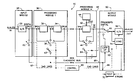
Referring now to Fig. 1 a digital signal processox
10, such as a digital video ef~ects generator, has a
plurality o~ modules which make up a signal path. ~n
input module 20 receives an analo~ input ~ignal, such
as an analog video signal from a camera, ~ideo tape
recorder or the like, and co~vert~ the analog ~ignal
to a digital ~ignal in ~n a~nal`og to digital con~rter
22. The resulting digit~l si~nal i~ input to a ~irst
proces~ing module 30 wher~ Yarious manipulations are
performed upon the digital ~ignal, ~uch a~
deinterlaclng, transfor~at~ons, etc., by various
circuits 32, 34. ~he output o~ the irst processing
module 30 is input to subse~uent processing modu~es
for additional ~i~nal processing. The output ~rom the
Nth proce~sing modu~e 40 ~ ~nput to an output module
50 where the pro~essed digital signal is converted to
- 5 - .
an analog output, such as a processed video picture,
by an digital to analog conYerter 52 fsr subsequent
display on a monitor. A timing circuit 54 also
receives a portion of the processed digital signal
which contains timing data synchronized with the
digital signal to provide timing signal inputs, such
as horizontal and vertical sync pulses for a
television system, to the D/A converter 52 as are
appropriate to provide a recognizable, stable display
of the analog output.
A service person interacts with a diagnostic
system incorporated into the digital signal processor
10 via a controller 60. ~he controller 60, or
operator interface, may consist of ~ront panel
switches, which provide input to an internal
microprocessor, or a computer terminal connected to
the digital signal processor 10. The diagnostic
system has a diagnostic bus 66 which is connected to
plurality of module selection 6witches 6~, 63, 64~
For modules with more than one internal test point, a
test point selection switch 36, 46 is provided Por
each module, the test point selection switch beiny
connected in turn to the respective modul~ selection
switch 63, 64. As shown in Fig. 1 the ~nput module 20
has a single test poi~tlTP~ .the output of,rt~e A/D
converter 22 which i~ ~onnected to the input module
select switch 52. Th~ ~irst processing module 30 h~s
three test points TP3 1, - TP3 3, TP3 5 at the respective
~nputs and outputs o~ the int~rnal circuits 32, 34,
which test points are con~ected to the ~irst
processing module test point selection swikch 36.
~ikewise the Nth processing module 40 has illu~trated
three test points TP41, TP43, TP45 at tha input and~or
output o~ respective lnternal circuits 42/ 44, which
~ ,
.....
.. . .
test points are connected to the Nth processing module
test point select~on 6witch 46. As ~s shown not all
circuits being monitored process the digikal signal.
For exampla the circuit 44 in the Nth p_ocessing
module represents a general function generator which
might provide an input to processing circuit 42. Thus
upon appropriate operator input to the controller 60,
or automatically, any test point within the digital
signal processor 10 may be connected to the diagnostic
bus 66. However, by an appropriate interlocking
structure, as is well known in the art, only one test
point can be connected to the diagnostic bus at any
given time.
In the output module S0 an output diagnostic
switch 65 selects the input for processing by the
output module. In normal op~ration the processed
digital signal is connected via the diagnostic switch
65 to the D/A converter 52 and ti~ing circuit 54.
~owever, during diagnostic vperation the diagnostic
bus ~6, vla a diagnostic transfG~mation circuit 68, is
connected to the D/A converter 52 and timing circuit
54 via the diagnostic switch 65. Thus any o~ the
internal test pointR can ~e displayed at the output o~
the digital signal proce~sor 10 by a service per~on
without int~rrupting the~~Aternal di~ital pro~e~sing
o~ the processor. The controller 60 is connected ~ia
appropriate command lines 67, 69 to the switches, the
diagnost~c transfsrmation circuit 68, and th~ timing
clrcuit 54. It ~hould be noted that th~ test point
and corre~pond$ng module electio~ ~witches may b~
combined into a single switch, a~ is evident to one
skilled in the art. ~180 output fr~m the output
module 50 is a STROBE pulse ~rom the timing circuit 54
to provide a trigger t~ an external test instrument
1 ;'
.
. ~
- 7 -
70, ~uch as a logic analyzer, which is connected tothe diagnostic bus 66, the STROBE pul~e corresponding
to a particular sample or p~xel within the digital
signal.
~ often the ~ase that several different forms
of ~ignals may exist within the digital ~ignal
processor 10 that need to be monitored. These signals
may vary in format, le~el and/or transmis~ion mode.
When a com~on output monitor is used, æuch as a
television video screen, it is desirable to translate
one or more of these di~ferent signals to a common
format ~o that the operator gets a visual
representation of the various ~ignals without having
to readjust the monitor for each different format.
For example in video processing a key signal may Yary
in level as it pass2s ~rom ~tage ~o stage within the
processor 10. As shown ln Fig. 2 the signal ~rom the
diagnostic hu6 66 is input to a first register 92
w~thin the diagnostic transformation clrcuit 68. The
output Or the ~irst register 92 is output via a swikch
91 to a lookup table memo~y 80 which contains a
plural~ty of lookup tabl~s, including a unity ~able.
The ~election o~ the appropriate lookup table within
the lookup table memory 80, generally ~tored in RO~,
may be used to automatically iëvel shift the~utput of
the diagnostic bus 66 depending on the seleoted teck
point. The appropriat~ lookup table ~rom the lookup
table ~emory 80 may also be used to make a
~Imeaningful9~ display of non video in~ormation~ such as
addresses or control data. The output o~ the
diagnostic bus 66 ~or these ~unctions would be mapped
into a black to white d~splay that would be meanlngful
to the operatorO Another common form of si~nal to be
monitored is one in which two independent wa~e~orms
,
,. .
. ~, . ..
:: ~
~L27~
- 8 - .
have ~een time multiplexed together, such a~ the U and
V components of chromlnance in a television 6ignal.
It is usually more ~eaning~ul ~o an operator to be
able to exa~ine the component waveforms independently
than to look at the time multiplexed combination, so a
demultiplexer 90 ~s required. Although the
demultiplexer 90 is shown as part of the diagnostic
transfo~mation circuit 68, individua} demultiplexers
may be placed in each module prior to the respective
module ~witches to perform the demultiplexing and
interpolating ~unction of the digital signal from the
selected test point prior to the diagnostic bus 66.
Fig. 2 shows a combination demultiplexer and
interpolator for two way interleaved signals, the
interpolator being used to fill in the gaps between
demultiplexed samples, which may also be done by
reducing the output clock rate of the D/A ~ections and
following filters of the D/A converter 52 at the cost
of ~dditional complexity. The demultiplexer output
switch 91 alternates between the output of the first
register 92 and the output of a divider g4. When
switched to the output of the first register 92, the
output at the 6witch 91 i the input multiplexQd
sample delayed one clock cycle. When switched to the
output o~ the divider 9~ e output i8 th~ ayerd~e Or
two ad~acant common sample6 as developed by a second
register 96, an adder 98 and the divider 94 as is well
known to those in the art. Other syste~s could
alternately U5~ higher order interpolators and/or msre
comp~ex demultiplexers ~or multi~lexed signals o~
higher order, l.e., khree way, four way, etc.
A digital signal i~ subject to delays at each
processin~ ~tage throu~h ~he processor 10. When this
o~curs the output o~ the diagnostic bus 66 varies in
,''' : ,
. . .
- ' '''
.. , ~ -
~ g --
time relative to a ~ixed external point, such as the
lnput ~ignal, as various test point~ are selected.
This makes it difficult to monitor a given sample, or
pixel, as it traverses the processor 10 unles~ some
reference i5 used that also ~aries in time by the same
amou~t from test point to test point. Fig. 3 shows a
system by which a horizontal and vertical timing
reference, obtained from the diagnostic bus 66, is
used to drive a set of counters 100, 102 in
synchronization with the incoming diagnostic digital
signal. The horizontal counter loO is clocked by a
column, or pixel, clock ~rom the controller 60, and
the ~ertical countPr 102 is clocked by a row~ or line,
clock from the controller. The timing data, such as
horizontal and vertical sync, fro~ the d~agnostic bus
66 resets the counters 100, 102 which then count up.
Each test point provides to the diagnostic bus 66
timing data as well as the digital signal, the timing
data having been delayed the same amount as the
digital datat i~e., the timing data is in time sync
with the test psint digital ~ignal. The outputs o~
the csunter~ 100, 102 are decoded by a lookup table
and sync generator 10~ to give ~ome ~et of
synchronizing ~ignals, such as video ~ync. ~o obtain
the STROBE pul6e for use b~ external test inst.r;uments
70 the output o~ the counters 100, 102 are input to
respective oompara~ors 106, 108. The other input to
the comparator~ 106, 108 are X-position and Y-position
commands fro~ the controller 60 which d~fine the
sample or pixel upon which a trigger is desired. The
outputs of the comparator~ 106, 108 ar~ input to a
combining circuit 110 so that the STROBE pulse occurs
only when the desired sample is pr~sent on ~he
diagnostic bus 66. Al~o thQ timing cixcuit 54 shown
.
' . .~. ~
:... ,...~:..,. ,..,., .. ~
:' ' : ''
~7~S~
i~ Fig. 3 ~5 used for "two~dimensional" signals, such
as video. Other ~orms of ~ignals, ~uch as aud~o, may
only use one ~et of counters, or mora sets o~ counters
may be needed by more advanced signals. Although only
one signal path i~ shown in the Figures, in real~ty
each signal path may consist of one or mor~
components, such as luminance, chrominanGe and key in
a digital video effects ~ystem, with each component
having one or more parallel bits, usually 8-10 bits
plus synchronizing or timing bits.
In operation a service person decides whether or
not to turn on the diagnostic system via switch 65
when a ~ault is suspected, and determines which module
and test point within that module to connect to the
diagnostic bus 66 ~or display. The controller 60
automatically conditions the appropriate circuits
within the diagnostic transformation circuit 68 and
the timing circuit 54 to apply appropriate o~fsets,
timiny pulses and/or transformations to the signal on
the diagnostic bus 66 80 that the signal may be
appropriately displayed in a recognizable and 6table
manner. Alternatively the diagnostic system may
operate automatically upon initiation by the operatox
to sample eaah test point in turn and record the
resulting information.on ~e~~`est instrument~,7Q.
~ hus the present invention provides a diagnostic
system for digital signal processing equipment whi~h
monitors various internal:test points of the e~uipment
to allow a service person to ~uickly determine that
portion of the total proc~ssor circuitry wh~ch i8 the
source o~ a fault.
- ....
' ' '', ': - -,: ~ , .. ,. ~.