Note : Les descriptions sont présentées dans la langue officielle dans laquelle elles ont été soumises.
~27~
- 1 -
46/86
20.5.~6
La/SC
.
Device for the EMI testing of electronic systems
Field of the invention
The present invention relates to a device for the
EMI testing of electronic systems. "EMI" appears as an
abbreviation for "electromagnetic interference". The in-
vention relates, in particular, to such a device having
a TEM waveguide, which opens out in a pyramid shape and
which is closed by a wall of high-frequency peak absor-
bers and which exhibits an asymmetricaLly disposed, plate-
shaped inner line, which is connected through the absor-
ber wall to a number of terminal resistors.
Description of the prior art
A device of the abovementioned type has been con-
structed in the Institut fu'r naturwissenschaftlich-tech-
nische Analysen (Institute for Natural Science and Engin-
eering Analyses) of the Frauenhofer Gesellschaft in Eus-
kirchen, Federal Republic of Germany. The TEM waveguide
of this device is laterally open. It consists of an asym-
metr;c three-str;p l;ne arrangement.
For reasons associated w;th the emission of radia-
t;on, it can be operated only in a screened room. In it,
the ~all constructed of the high-frequency peak absor-
bers ;s s;tuated ;n the l;ne cross-section and is planar.
the inner line is suspended by nylon threads at the upper
strip line. In the reg;on of passage through the absor-
ber wall, the ;nner line tapers towards the terminal
res;stors. 6y th;s means, a compensat;on of the capa-
c;t;ve loading caused by the absorbers ;s achieved inrelation to the characteristic impedance. So-called light-
structure aluminum plates are employed in accordance with
the sandwich princ;ple as material for the ;nner line.
-- 2
The TEM waveguide of the device of the Frauenhofer Gesell-
schaft cannot be dismantled in the longitudinal direction.
The return loss achieved with this waveguide is better
than -15 dB up to a frequency of approximately 2.5 G~lz.
Description of the invention
An object of the present invention is to provide
a device of the initially mentioned type which, above all,
is improved with regard to its external space require-
ment in relation to the useful test volume. The test
volume should be able to accommodate at least one indivi-
dual, relatively small sw;tch cabinet of the size cus-
tomarily used nowadays.
A further object of the present invention is to
provide a device of the initially mentioned type which is
improved with respect to its wave transmission proper-
ties.
The said objects as well as other objects areachieved according to the present invention by the provi-
sion of a novel device for the EMI testing of electronic
systems having a TEM waveguide, which opens out in a
pyramid shape and which is closed by a wall of high-fre-
quency peak absorbers and which exhibits an asymmetrically
disposed, plate-shaped ;nner l;ne, wh;ch is connected
through the absorber wall to a number of terminal resis-
tors; the TEM waveguide further exhibits a closed outer
line, and the absorber wall is curved in the manner of a
spherical segment, the center of curvature being situated
in the region of the t;p of the pyramid-shaped TEM wave-
guide~
As a result of the closed outer line of the TEM
waveguide, the device accord;ng to the invention is prac-
t;cally free from extraneous emission of radiation to theenvironment. Accordingly, it does not need to be opera-
ted in a screened area, but can be set up directly at
any selectable location, without restriction. Accordingly,
it is the external dimensions of the TEM waveguide and
not those of a screened area which determine the space
:
~ 3~
-- 3
requirement of the device. With the device according to
the invention, the ratio of space requirement to useful
test space volume is optimized to a very great extent.
As a result of the design of the absorber wall
in the manner of a spherical segment, differing transit
paths and transit times for the electromagnetic waves
are avoided in the TEM waveguide. Resonance problems
which are per se to be expected in a TEM waveguide with a
closed outer tine of the size under consideration here do
not occur. In addition to this, an excellent field homo-
geneity in tne test value over the entire frequency range
is achieved. The same applies to the return loss.
Even more far-reaching improvements can be
achieved by means of the measures defined in the appen-
dant patent claims.
Thus, it is of advantage to divide the inner tineinto a plurality of partial lines in the region of passage
through the absorber wall, in which its width must be
r_duced in order to compensate the capacitive effect of
the absorbers on the characteristic impedance, and in
each instance to taper the width of the partial lines to-
wards the terminal resistors. By this means, transverse
components of the field in the terminal region, which
cause field distortions and reflections, are reduced to
a very small amount. ~ith a device according to the in-
vention which is designed in this manner and which has a
length of 6.5 m, an overall height of 1.5 m and a width
of 3 m, it vas possible to achieve a return loss of bet-
ter than -20 d~ over a frequency range of 0 Hz to approxi-
mately 2.5 GHz. A value of better than 10 d8 could bedetermined in the said frequency range for the homogeneity
~fluctuation vidth) of the electromagnetic field.
By means of a design of the TEM waveguide with a
removable feed wedge which is gas-tight on all sides and
which is capable of withstanding excess pressure and which
can be filled with SF6 gas, the device according to the in-
vention can also be des;gned so as to be suitable for extre-
mely high f;eld strengths. In addition, high-tension resis-
tors can be employed as terminal resistors for this purpose.
73~
Elrie~ description of the drawing
Further features and advantages of the present
invention are evident from the detailed description ~hich
follows, in particular with reference to the accompanying
drawing. The drawing shows, in a single figure, a pers-
pective view of a device according to the invention hav-
ing a TEM waveguide which opens out in a pyramid shaPe.
Best manner of implementation vf the invention
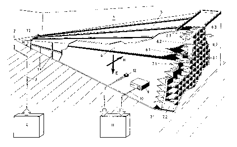
Reference is now made to the drawing. In the
drawing, reference numeral 1 designates a TEM waveguide.
"TEM" appears as an abbreviation for "transverse electro-
magnetic". The TEM waveguide 1 opens out in a pyramidshape from its tip 2. It does not exhibit any kinks.
Although this is not discernible in the drawing, at its
tip 2 a coaxial feed bushing is provided, via which a
pulse or s;nusoidal generator 4 can be connected to the
TEM waveguide 1 by means of a coax;al cable 3.
The TEM waveguide exhibits a closed outer line S
having a rectangular cross-section. A plate-shaped inner
line 6 of triangular shape is suspended in its interior
asymmetr;cally on nylon threads. "Asymmetrically" means
that the inner line 6 exhibits a smaller spacing from the
top of the outer line 5 than from the bottc,m thereof. As
a result of this asymmetry, there is in the lower part of
the TEM waveguide 1 a greater useful test volume than if
the inner line 6 were disposed symmetrically. This ar-
rangement also results in a smaller reaction of the elec-
trical systems to be tested on the electromagnetic f;eld~
Preferably, the spacing of the inner line 6 from the top
of the outer line 5 amounts to one quarter of ;ts respec-
tive height. Correspondingly, the spac;ng of the ;nner
l;ne 5 from the bottom or baseplate of the outer line 5
amounts to three quarters of its respective height.
Having regard to the asymmetric arrangement of
the inner line 6 and the outer line 5, the widths of these
are selected in their rat;o to one another in such a manner
~ ' .
3~
5 --
that a characteristic impedance corresponding to the pulse
generator or to the sinusoidal generator 4 and naturally
also to the coaxial cable 3 is created for the TEM wave-
guide 1. At an aperture angle of 20 and the preferred
asymmetry of 1~4:3/4, a characteristic impedance of S0 ohms
is created, for example, by a width ratio of 0.636~
As has already been mentioned, the inner line 6
is suspended by means of nylon threads at the top of the
outer line 5. A fine tuning of the characteristic impe-
dance is possible by a slight variation of the length ofthese nylon threads and thereby also of the abovementioned
asymmetry.
The TEM waveguide 1 is closed on the one hand by
a plurality of mutually adjoining pyramid-shaped high-
frequency peak absorbers 7.1 which in their entirety forman absorber wall 7, and on the other hand by three ohmic
terminal resistors 8.1, 8.2 and 8.3. The high-frequency
peak absorbers 7.1 and the terminal resistors 8.1, 8.2
and 8~3 are complementary in their closing effect. The
latter form the effective termination of the TEM wave-
guide for frequencies below approx;mately 100-200 MHz.
The high-frequency peak absorbers are designed, as regards
their shape and size, in such a manner that they come into
effect above 100-200 MHz.
The absorber wall 7 is curved in the manner of a
spherical segment. The center of curvature is situated
in the reg;on of the t;p 2 of the TEM waveguide. As a
result of this curvature, differing trans;t paths and
transit times of the electromagnetic waves in the TEM
waveguide 1 are avoided.
The peak absorbers 7.1 preferably consist of poly-
urethane foam, which is compounded with conductive par-
ticles, e.g. of carbon in the form of graph;te or soot.
In spite of this compounding with the conductive material,
the absorbers 7.1 as a whole exhibit relatively poor con-
ductivity. As a result of their finite conductivity and
their pyramid shape, HF energy is converted into heat in
them. Their peak height should amount to approximately
1/3 of the height of the outer line S at its opened-out
~3~
end, and the ratio of peak height to base surface area
should amount to approximate(y 6.5:1~ As shown in the
drawing, the absorber wall 7 or the peak absorbers 7n 1
can be supported by a box-like structure 7~2~ The inner
line 6 is connected to the terminal resistors 8.1, 8.2
and 8.3 by the absorber wall 7 ~ passing through between
two rows of absorbers 7.1 - with splitting into three
separate parallel partial lines 6~1, 6.2 and 6.3; in this
connection, a terminal resistor is connected at each of
the partial lines 6.1, 6.2 and 6.3 The terminal resis-
tors 8.1, 8.2 and 8.3 connect the inner tine or its par-
tiat lines 6.1, 6.2 and 6.3 to the outer line 5.
The position of separation of the inner line 6
into the partial lines 6.1, 6.2 and 6.3 is situated app-
roximately at the height of the peaks of the absorbers7~1~ The splitting of the inner line 6 into the three
partial lines 6.1, 6.2 and 6.3 is undertaken in such a
manner that the same surface charge or the same partial
characteristic impedance is allocated to each one of the
three partial lines in the waveguide. The terminal resis-
tors 8.1, 8.2 and 8.3 can then be dimensioned consistently,
in a manner corresponding to this partial characteristic
impedance. ln this case, the central partial l;ne 6.2 is
at first wider than the two outer ones 6.1 and 6~3.
The three partial lines 6.1, 6.2 and 6.3 taper
acutely towards the terminal resistors 8.1, 8.2 and 8.3.
In this connection, the taper of their width is provided
in each instance in such a manner that the capacitive
covering which is caused by the absorbers 7.1 and which
increases towards the terminal resistors in the absorberwall 7 as a result of their peaks or pyramid shape is
compensated in its efFect on the characteristic impedance
or partial characteristic impedance.
The TEM waveguide 1 can be made in the form of a
light construction. Light weight aluminum plates suppor~
ted by aluminum profiles 1.1 can be employed as material
for the outer line in accordance with the sandwich prin-
ciple. This material offers not only a low weight and a
high degree oF stiffness but also the advantage that it
.
,,,
can be processed off the roll. The lateral parts of the
outer line can thereby be constructed from a single piece,
without butt joints. This is of advantage with regard
to the avoidance of reflections. An aluminum sheet or a
galvanized steel sheet can be employed as material for
the inner line. Furthermore, the final third of the base-
plate of the outer line S in front of 'he absorber wall
7, on which outer line the electronic systems to be tested
such as the system 9 shown in the drawing as a rule stand,
can be reinforced by a galvanized steel sheet.
In order to provide convenient access to the
interior of the TEM waveguide 1, a door can be provided
in one of the lateral walls of the outer line 5. This
door is preferably a sliding door.
In addition to having good wave propagation pro-
perties, the TEM waveguide should also be sufficiently
resistant to h;gh voltages, in order to permit testing
using NEMP field strengths of 50 kV/m. "NEMP" appears
as an abbreviation for the so-called "nuclear electro-
magnetic pulse". With unchanged geometry, the resistance
to high voltages of the TEM waveguide 1 can be increased
substantially by filling the waveguide not with air but
instead with an electronegative gas such as, for example,
SF6 at a pressure which is as high as possible. In the
case of the preferred overall length of the TEM waveguide
1 of over 6 m and the preferred light construction, this
;s not, however, possible without further ado~ It is,
of itself, also not required, s;nce flashovers or break-
downs are to be expected only ;n the reg;on of the tip of
the TEM wavegu;de 1, more precisely at the place of tran-
s;t;on from the coax;al feed socket, wh;ch ;s as a rule
f;lled w;th a sol;d ;nsulator, to the gas-f;lled wavegu;de.
It ;s therefore suff;cient to design the tip reg;on or
the feed wedge of the TEM wavegu;de 1 ;n an appropr;ate
manner. Preferably, the feed wedge of the TEM wavegu;de
1 is constructed as a separate component part 1 2, wh;ch
is releasably secured to the remain;ng part of the TEM
waveguide 1, closed ;n a gas~t;ght manner on all s;des
and capable of be;ng subjected to excess pressure~ The
:L~73C~
volume of the removable feed wedge 1.2 is sealed ln
relation to the remaining volume of the TEM waveguide
1 by means of a thin dielectric foil which alters the
high-frequency properties to the smallest exten-t
possible. The longitudinal extent of the feed wedge
1.2 need be only approximtely 1/10 of the overall
length of the TEM waveguide 1.
Having regard to the resistance of the TEM
waveguide 1 to high voltages, it is possible, by way
of a supplementary matter, to construct the terminal
resistors as high-tension resi~tors. They should be
designed for at least 100 kVo However, high~tension
resistors are naturally long, and exhibit a con-
siderable inductivity as a resul-t of their overall
:Length. This makes them unsuitable, of themselves,
for use as high-frequency terminal resistors. High-
frequency terminal resistors should be as short as
possible and should exhibit low inductivity. In the
case of resistors, good high-tension properties and
hi~h-frequency properties are mutually exclusive. In
spite of this problem, high-tension resistors can be
employed in the device according to the invention,
because they are required and must be effective as
terminal resistors only up to approximately 100-200
MHz. Above 200 MHz, as has been explained, the
efEective termination of the TEM waveguide 1 is
formed by the high-fre~uency peak absorbers 7.1. In
terms of power, the termi.nal resistors should be
designed Eor a CW power o:E up to 1 kW.
From the e.l.ectron:ic system, such as the
system 9 in the drawing, which is introduced into the
TEM waveguide 1 and which is to be tested, measure-
~ ment lines 10 lead out of the TEM waveguide to
:: .
'~
.
.: - ; ~.............. .:
.
. .
~. . ~:.. :. ,
~;~7~
appropria-te measuring ins-truments 11. Field sensors
12 can also be connected to these, by means of which
field sensors -the strength oE -the electromagnetic
field is measured in the TEM waveguide 1 in the
vicinity of the electrical system 9 to be -tested.
Instead of being used for testing the
effect of electromagneti.c fields on electronic
systems, the device according to the invention can
also be employed for measuring the radiation emitted
by an electronic~system.
~"~f1~