Sélection de la langue

Search

Sommaire du brevet 1273130 

Énoncé de désistement de responsabilité concernant l'information provenant de tiers

Une partie des informations de ce site Web a été fournie par des sources externes. Le gouvernement du Canada n'assume aucune responsabilité concernant la précision, l'actualité ou la fiabilité des informations fournies par les sources externes. Les utilisateurs qui désirent employer cette information devraient consulter directement la source des informations. Le contenu fourni par les sources externes n'est pas assujetti aux exigences sur les langues officielles, la protection des renseignements personnels et l'accessibilité.

Disponibilité de l'Abrégé et des Revendications

L'apparition de différences dans le texte et l'image des Revendications et de l'Abrégé dépend du moment auquel le document est publié. Les textes des Revendications et de l'Abrégé sont affichés :

  • lorsque la demande peut être examinée par le public;
  • lorsque le brevet est émis (délivrance).
(12) Brevet: (11) CA 1273130
(21) Numéro de la demande: 1273130
(54) Titre français: ADAPTATEUR DE SONDAGE POUR PRISE DE PORTE-PUCE
(54) Titre anglais: TEST POINT ADAPTER FOR CHIP CARRIER SOCKETS
Statut: Périmé et au-delà du délai pour l’annulation
Données bibliographiques
(51) Classification internationale des brevets (CIB):
  • G01R 01/04 (2006.01)
(72) Inventeurs :
  • RENNER, ROBERT EDWARD (Etats-Unis d'Amérique)
  • KUTZ, DAVID ALAN (Etats-Unis d'Amérique)
(73) Titulaires :
  • GTE COMMUNICATION SYSTEMS CORPORATION
(71) Demandeurs :
  • GTE COMMUNICATION SYSTEMS CORPORATION (Etats-Unis d'Amérique)
(74) Agent: R. WILLIAM WRAY & ASSOCIATES
(74) Co-agent:
(45) Délivré: 1990-08-21
(22) Date de dépôt: 1987-06-15
Licence disponible: S.O.
Cédé au domaine public: S.O.
(25) Langue des documents déposés: Anglais

Traité de coopération en matière de brevets (PCT): Non

(30) Données de priorité de la demande:
Numéro de la demande Pays / territoire Date
876,070 (Etats-Unis d'Amérique) 1986-06-19

Abrégés

Abrégé anglais


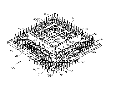
TEST POINT ADAPTOR FOR CHIP CARRIER SOCKETS
ABSTRACT OF THE INVENTION
This arrangement provides for attaching test or probe
leads for such instruments as a logic analyzer to a leaded chip
carrier. This arrangement provides for terminating each chip
carrier lead to a metallic post upon which a logic probe or other
test apparatus may be mechanically attached to make electrical
connection. Since leaded chip carriers have their contact leads
closely spaced, this arrangement expands this distance between
leads to a suitable distance for connecting test probes. In this
manner, the semiconductor chip may be functionally tested as part
of a circuit on a printed wiring card.

Revendications

Note : Les revendications sont présentées dans la langue officielle dans laquelle elles ont été soumises.


WHAT IS CLAIMED IS:
1. A test point adaptor for permitting an electrical
connection of a test probe apparatus to a semiconductor chip
mounted in a semiconductor chip carrier, said chip carrier
including a plurality of connecting pins electrically connected to
said semiconductor chip extending from said chip carrier, said
test point adaptor comprising:
a circuit board having a pluralitiv of conductive foil paths,
each conductive foil path connecting a corresponding inner foil
pad to a corresponding outer foil pad;
first terminal means connected to said circuit board, said
first terminal means including a plurality of electrically
conductive pin members, each pin member electrically connected to
a corresponding inner foil pad;
said first terminal means further including a plurality of
electrically conductive pin accepting members, each pin member
electrically connected to an associated first terminal means pin
member and each pin accepting member is arranged to accept a
respective and associated chip carrier connecting pin, therein,
connecting said circuit board and said foil paths to said chip
carrier with said semiconductor chip: and
second terminal means connected to said circuit board, said
second terminal means including a plurality of electrically
conductive pin members, each of said second terminal means pin
members connected to a corresponding outer foil pad of said
circuit card, said second terminal means pin members providing for
selective electrical connection of said test probe apparatus to
said semiconductor chip in said leaded chip carrier.
2. A test point adaptor as claimed in claim 1, wherein there
is further included third terminal means including a plurality of
electrically conductive pin accepting members, each of said third
terminal means pin accepting members is connected to a corre-
sponding pin member of said first terminal means, and said third
terminal means further including a plurality of pin members
electrically connected to an associated pin accepting member, each
of said pin members of said third terminal means being further
connectable to printed wiring card means.

3. A test point adaptor as claimed in claim 2, said printed
wiring card means is a master printed wiring card assembly used
for in circuit testing of said semiconductor chip.
4. A test point adaptor as claimed in claim 3, said first
terminal means comprises a plurality of terminal strip devices
each of said terminal strip devices including at least one
electrical socket for accepting a pin therein, and a terminal pin
electrically connected to an associated socket extending from said
terminal strip device.
5. A test point adaptor as claimed in claim 4, said
connection of said terminal strip device terminal pins to each of
said inner foil pads includes a soldered connection.
6. A test point adaptor as claimed in claim 5, said second
terminal means comprises a plurality of terminal strip devices,
each said terminal strip device including first and second
terminal pins, and each first terminal pin electrically connected
to an associated second terminal pin, and each second terminal pin
connected to a corresponding outer foil pad, and each first
terminal pin arranged to accept and make an electrical connection
to said test probe apparatus.
7. A test point adaptor as claimed in claim 6, said
connection of said terminal strip device second terminal pins to
each of said outer foil pads includes a soldered connection.

Description

Note : Les descriptions sont présentées dans la langue officielle dans laquelle elles ont été soumises.


1273~
TEST POINT A~APTER FOR CHIP CARRIER SOCKETS
BACKGROUND OF THE INVENTION
This invention pertains to electronic testing of socket
mounted semiconductor chips and more particularly to electronic
testing of chips in sockets with a large number of leads which are
closely positioned.
One packaging type for integrated circuits is a leaded
chip carrier (LCC) type. The LCC has leads on all four sides with
spacing in between of 0.050 inch. Sockets for mounting a chip
carrier to a printed wiring card do not provide any means for
attaching testing apparatus leads. The chip carrier itself does
not allow for physically attaching any test probe apparatus. Most
test leads, such as logic analyzer probes, require 0.100 inch
spacings between test points.
Another type of integrated circuit package is the dual
in-line package (DIP). The DIP chips have leads on only two sides
with pins spaced at 0.100 inch. Commercially available DIP clips
(like clothes pins) may be clipped directly onto the chip leads in
order to perform testing. These clips provide relatively long
pins to which a logic probe may be attached. No clip type device
can be adapted to a four sided LCC package when the LCC package is
mounted in a suitable socket.
SUMMARY OF THE INVENTION
A test point adaptor permits connection of a test probe
to the leads of a semiconductor chip which is mounted in a leaded
chip carrier. Electrical connection may not be made directly to
the semiconductor chip while it is mounted in the leaded chip
carrier.
The test point adaptor includes a circuit board whlch
has a number of conductive paths. Each conductive path is
connected between an inner point of the circuit board and an outer
point of the circuit board.
A first connector array is mounted to the circuit
board. The first connector array has a number of terminal pins.
Each of the terminal pins is connected to a corresponding inner

3L~7 3 l~O
polnt of a particular conductive pa~h. ~he first connector arra~
is also connected to the leaded chip carrier which contains the
semicon~uctor chip.
~he test point adaptor also has a second connector
array. The second connector array is mounted to the circuit
board. me second connector array has a nNmber of terminal pins,
each of which is connected to a corresponding outer point of a
corresponding conductive path.
The test probe may now be connected to any of the
termlnal pins of the second connector to obtain electrical aocess
for testing the semiconductor chip which is mcunted in the leaded
chip carrier.
A ~RIEF DESCRIPlION OF TEIE I~1INGS
Figure 1 is an assembly drawing of test point adaptor
embodying the principles of operation of the present invention.
Figure 2 is a layout of the foil paths of the printed
wiring card of Figure l.
DESCRIPqION OF THE PRSFERRED EMBODIMENT
Referring to Figures l and 2, a chip carrier 20 is shown
mcNnted on a test point adaptor 100. The printed wiring card 10
is an approxImately tw~ (2) inch square. m e chip carrier 20 is
approximately one and three-sixteenths inch square. m ere are
seventeen (17) connection points on each side of the chip carrier
square. The printed wiring card 10 allows electrical contact to
be made along the two inch square side.
The printed wiring ¢ard 10 has foil paths 30 which allaw
widening of the distanoe between conductors 40 on the chip carrier
20 from 0.050 inch to 0.100 inch required for attaching a lagic
prcbe. The printed wiring card 10 includes a plurality of foil
paths 30 connecting respective inner foil pads 32 to auter foil
pads 34. Each foil pad 32 and 34, includes a centrally lacatad
hole (nok shown) e#tendin~ thru the printed wiring card 10. A
plurality of terminal strip devioes 50 are installed on the
printed wiring oard 10. Each terminal strip devioe includes a row
of pin receiving portions or sockets 51 and a row of pins 52.
Each socket 51 is integrally joined to an associated terminal pin
52 which extend outward directly opposite fram its associated
socket 51.

~ ~7~
Each pin 52 is arranged to be inserted through a
respective drilled hole of each mner foil pad 32. me inner foil
pads 32 are grcuped into tT~o side-by-side rows on each side of a
square perimster. me inner row accepts an eight pin termm al
strip device 50 and the outer row of each side of the square
contains a nine pin terminal strip device 50. m ese pin strips
are manufactured by Samtec and are part no. SS-101-G-~.
Electrical connection is made between the pins 52 and
the foil pads 32 by soldering. This soldering operation also
provides for mechanical stability of the terminal strip devices 50
and the printed wiring card 10.
me outer foil pads 34 are arranged into four linear
groups with each group extending longitudinally along a respective
perimeter edge of wiring card 10. Terminal strip devices 60
having upper and lower pins 61 are mounted to the printed wiring
card 10 by having the lower pins 61 (not shown) inserted through a
respective and associated drilled hole on the top of wiring card
10, thereby, allowing each lower pin 61 to extend thru the circuit
card and exit from an associated foil pad 34 on the bottom of the
2~ circuit card. m ese large t~rminal strip pins are part no.
TSW-136-070-G-S manufactured by Samtec. A strip of these terminal
strip devices 60 include seventeen pins (17). me upper pins 61
are a sufficient distance apart (0.100 inch) to permit the
connection of test probes to test the functiQns of the
semiconductor chip (not shown) contained in the chip carrier 2C.
A test prQbe such as a part no. 010-6451-00 may be connected to
upper pins 61. me test probe mentioned above is Don=f:cturei by
the Tektronics Corporation and may be plugged into a logic
analyzer model no. 7D01 also manufactured by Tektronics.
me lower pins 61 of the terminal strip device 60 are
soldered to a respective foil pad 34. This soldering also
provides for a stable connection of the termin~l strip devices 60
to the printed wiring card.
Next, the chip ~rrier 20 may be inserted into the
terminal strip devices 50. me integrated circuit chip (not
shown) may have keen previcusly inserted into the chip carrier 20
or chip carrier 20 may be removed and another chip fitted into the
chip carrier 20. The pins 22 of the chip carrier 20 must be
' 3

~7~
carefully aligned with the female opening of the terminal strip
devices 50, so that the chip carrier pins 22 do not flex or bend
and are all evenly seated and the chip carrier 20 urged downward
inserting each pin 22 into a respective and associated socket 51
to make sufficient electrical contact.
Lastly, a third set of terminal strip devices 70
identical to termlnal strip devices 50, have their sockets 71
connected to a respective and associated pin 52 of terminal strip
devices 50. The pins 72 of terminal strip devices 70 are part no.
SS-lol-G-2 and are also manufactured by Samtec. me pins 72 of
terminal strip devices 70 extend fram the bottam of printed wiring
card 10 and facilitate the mountLng of the completed adaptor
assembly 100 containing the chip carrier 20 to a master printed
wiring card (not shown), so that the resulting master printed
wiring card assembly may be tested and the semiconductor chips
easily inserted, remcved or changed.
Although the preferred embodiment of the invention has
been illustrated, and that form descr;hc~ in detail, it will be
readily apparent to those skilled in the art that various
modifications may be made therein without departing from the
spirit of the invention or from the scope of the appended claims.

Dessin représentatif
Une figure unique qui représente un dessin illustrant l'invention.
États administratifs

2024-08-01 : Dans le cadre de la transition vers les Brevets de nouvelle génération (BNG), la base de données sur les brevets canadiens (BDBC) contient désormais un Historique d'événement plus détaillé, qui reproduit le Journal des événements de notre nouvelle solution interne.

Veuillez noter que les événements débutant par « Inactive : » se réfèrent à des événements qui ne sont plus utilisés dans notre nouvelle solution interne.

Pour une meilleure compréhension de l'état de la demande ou brevet qui figure sur cette page, la rubrique Mise en garde , et les descriptions de Brevet , Historique d'événement , Taxes périodiques et Historique des paiements devraient être consultées.

Historique d'événement

Description Date
Inactive : CIB expirée 2020-01-01
Inactive : CIB désactivée 2011-07-26
Inactive : CIB de MCD 2006-03-11
Le délai pour l'annulation est expiré 2003-08-21
Lettre envoyée 2002-08-21
Accordé par délivrance 1990-08-21

Historique d'abandonnement

Il n'y a pas d'historique d'abandonnement

Historique des taxes

Type de taxes Anniversaire Échéance Date payée
TM (catégorie 1, 7e anniv.) - générale 1997-08-21 1997-08-20
TM (catégorie 1, 8e anniv.) - générale 1998-08-21 1998-08-13
TM (catégorie 1, 9e anniv.) - générale 1999-08-23 1999-08-03
TM (catégorie 1, 10e anniv.) - générale 2000-08-21 2000-08-21
TM (catégorie 1, 11e anniv.) - générale 2001-08-21 2001-08-13
Titulaires au dossier

Les titulaires actuels et antérieures au dossier sont affichés en ordre alphabétique.

Titulaires actuels au dossier
GTE COMMUNICATION SYSTEMS CORPORATION
Titulaires antérieures au dossier
DAVID ALAN KUTZ
ROBERT EDWARD RENNER
Les propriétaires antérieurs qui ne figurent pas dans la liste des « Propriétaires au dossier » apparaîtront dans d'autres documents au dossier.
Documents

Pour visionner les fichiers sélectionnés, entrer le code reCAPTCHA :


Pour visualiser une image, cliquer sur un lien dans la colonne description du document. Pour télécharger l'image (les images), cliquer l'une ou plusieurs cases à cocher dans la première colonne et ensuite cliquer sur le bouton "Télécharger sélection en format PDF (archive Zip)" ou le bouton "Télécharger sélection (en un fichier PDF fusionné)".

Liste des documents de brevet publiés et non publiés sur la BDBC .

Si vous avez des difficultés à accéder au contenu, veuillez communiquer avec le Centre de services à la clientèle au 1-866-997-1936, ou envoyer un courriel au Centre de service à la clientèle de l'OPIC.


Description du
Document 
Date
(aaaa-mm-jj) 
Nombre de pages   Taille de l'image (Ko) 
Abrégé 1993-10-07 1 15
Revendications 1993-10-07 2 81
Dessins 1993-10-07 1 53
Description 1993-10-07 4 161
Dessin représentatif 2002-03-06 1 28
Avis concernant la taxe de maintien 2002-09-17 1 177
Taxes 1999-08-02 1 36
Taxes 2001-08-12 1 40
Taxes 2000-08-20 1 34
Taxes 1996-07-30 1 53
Taxes 1995-08-15 1 52
Taxes 1994-08-02 1 53
Taxes 1993-07-29 1 37
Taxes 1992-08-03 1 41