Note : Les descriptions sont présentées dans la langue officielle dans laquelle elles ont été soumises.
U60-128,380
ELECTRONIC CARD CONNECTING CIRCUIT
This invention relates to an electronic card
connecting circuit for use in a receiving device for
cards having elec~ronic functions, and more particularly
to a control for supplying power to an electronic card
os incorporating therein integrated circuits (which are
referred to as "IC" hereinafter) to be inserted into
an electronic card receiving device.
With the recent development of the IC
technique, it has become possible to realize the IC on
0 a large scale in a small chip. As a result, various
kinds of such products having high degree functions
have been developed and their applications have been
widely extended.
For example, particular cards have been
manufactured in which are embedded read-only memory (ROM)
including programs written therein of microprocessors
or the like and random access memory (RAM) capable of
~; taking in and out data.
Moreover, electronic equipment incorporating
microprocessors or the like therein have been minia-
turized to pocketable sizes. With such miniaturized
equipment, the requirement of using cards incorporating
~; therein IC has been increased.
For example, there is a tendency for so-called
- 2 - ~l,
~ ~7 ~ ~ 5
"credit cards" or "cash cards" used in financial systems
to incorporate therein IC. Therefore, it has been
required to miniaturize the equipment using such
electronic cards to pocketable sizes.
05 In case o~ using such electronic cards, many
connecting contacts between the card and electronic
equipment are arranged side by side on part of a card
including a printed circuit board (which is referred to
hereinafter "PCB"). The power is supplied from the
0 electronic equipment through the connecting contacts to
the electronic card. The electronic card is generally
so mishandled that it is likely to be dirty and damaged
in use, with the result that complete connection cannot
be obtained and the electronic equipment is devoid of
reliability.
When an electronic card is inserted in
an electronic card receiving device of an electronic
equipment, ground and power source terminals of the
electronic card are connected together with input and
output terminals for other signals to the electronic
equipment, so that the electronic card performs i-ts
operation with the aid of the supplied power. In this
case, however, many connecting contac-ts are seldom
connected simultaneously to the equipment. Accordingly,
for example, if the power source terminal is first
connected and then the ground terminal is connected,
contents of the built-in ROM and RAM are often changed
or in extreme cases are damaged. Particularly,
~ ~7~ 2~ ~
electronic cards having cells or batteries therein are
likely to cause such troubles.
In order co avoid these troubles, it has been
proposed to connect the ground terminal first and
05 thereafter the power source terminal when an electronic
card is inser~ed into an electronic card receiving
device, and to disconnect the ground terminal finally
when the electronic card is removed from the device.
However, the power source terminal is often connected
0 before the ground terminal is connected sufficiently,
due to unavoidable dirt or damage.
It is an object of the invention to provlde
an improved electronic card connecting circuit which is
reliable and eliminates all the disadvantages of the
prior art above described and which completely pre~ent
a power source from being connected to an electronic
card before a ground terminal of the card is earthed.
In order to achieve this object, the electronic
card connecting circuit according to the invention
comprises first contact means for earthing a ground
terminal of an electronic card~ second contact means
for electrically contacting said ground terminal to
detect said ground terminal being earthed by said first
contact means, and detection control means including
2s an active element which detects said second contact
means being connected through said ground terminal to
said first contact means and controls a power source
circuit to supply power to said electronic card.
~ 4 ~ ~
With this arrangement, when the first and
second contact pins or contact means are in contact
with the ground terminal of the electronic card, in
other words, the earthed first contact pin is in contact
oS with the ground terminal of the card and the second
contact pin is contact with ground terminal and thus
earthed, the control means detects the second contact
pin being earthed to produce a control signal to apply
power of source to the electronic card. In this manner,
0 the problem that the power source is connected to the
card before the ground terminal of the card is earthed
can be eliminated.
The invention will be more fully understood
by referring to the following detailed specification
and claims taken in connection with the appended
drawings.
Fig. 1 is a circuit arrangement illustrating
one embodiment of the invention; and
Figs. 2a, 2b and 2c are circuit arrangements
illustrating other embodiments of the invention.
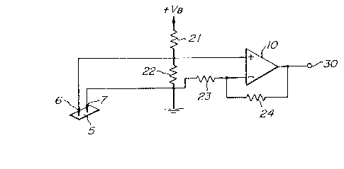
Referring to Fig. 1 illustrating one embodiment
of the invention, reference numeral 5 denotes a ground
terminal among a number of terminals of an electronic
card. Contact pins 6 and 7 of an electronic card
2s receiving device for an electronic equipment are in
contact with the ground terminal 5. A circuit shown in
Fig. 1 comprises an operational amplifier 10 and
resistors 21-2~. The operational amplifier 10 has
~ 2~
an output terminal 30. A power source is indicated
by +V
It is assumed that the power source ~VB is o~
for example ~5 V, the resistors 21 and 24 are of for
05 example 100 KQ and the resistors 22 and 23 are of for
example 1 RQ.
The contact pin 7 is grounded to an earth of
the electronic card receiving device. The contact pin
6 is connected to a junction of the resistors 21 and 22
o and to one input terminal of the operational amplifier
having a plus sign. An output terminal 30 of the
operational amplifier 10 is fedback through the resistor
24 to the other input terminal of the operational
amplifier 10 having a minus sign.
When either or both the contact pins 6 and 7
are oat of contact with the ground terminal 5, the power
source +VB (+5 V) is divided by the resistors 21 and
22, so that an electric voltage of about 50 mV is
applied to one of the input terminals of the operational
amplifier, with the result that a voltage of the output
terminal 30 is for example approximately 5 V.
When Doth the contact pins are in contact
with the ground terminal 5, the resistor 22 is
short-circuited, so that the voltage of one input
terminal of the operational amplifier 10 is zero and
the voltage of the output terminal 30 is also zero.
The voltage of the output terminal 30 is impressed
to a power source circuit (not shown) to control the
- 6 -
circuit in a manner that when the voltage of the outputterminal 30 is about 5 V, the voltage is not impressed
to a power source terminal (not shown) of the electronic
card, and when the voltage of the output terminal 30 is
05 substantially zero, the voltage is impressed to the
power source terminal. Accordingly, lhe power source
voltage is not applied to the power source terminal of
the electronic card before the ground terminal 5 has
been grounded by means of the contact pin 7. Thereore,
0 an accident such as damage of contents of the electronic
card can be prevented.
Referring to Fig. l, even if only the contact
pin 6 is in contact with the ground terminal 5, the
voltage of the contact pin is low as approximately
50 mV by which the RAM and ROM o~ the electronic card
are not affected.
Other embodiments according to ~igs. 2a, 2b
and 2c will be explalned hereinafter.
A circuit shown in Fig. 2a comprises an NPN
transistor ll and resistors 25 and 26 connected as
shown in the drawing. It is assumed that a power
source voltage +V~ is +5 V and the resistors 25 and 26
.
are of lO KQ and lOO Kn, respectively. Either or both
cont~ct pins 6 and 7 are not in contact with a ground
~5 terminal 5, a base voltage of the ~ransistor ll is
about 0.7 V, so that the transistor ll is sufficiently
under an ON condition and therefore the voltage of -the
output terminal 30 is sufficiently low. When both the
~ 35
contact pins 6 and 7 are then brought into contact with
the ground tenminal 5, the base voltage of the transistor
11 becomes zero, so that the transistor 11 is turned to
OFF and the voltage of the output terminal 30 becomes
05 about 5 V. Accordingly, it may be so constructed that
only when ~he voltage of the output terminal 30 is
about 5 V, the power source voltage is impressed to the
power source terminal of an electronic card.
A circuit shown in Fig. 2b comprises an
o inverter 12 connected in the circuit shown in the
drawing. Only when contact pins 6 and 7 are in contact
with a contact terminal 5, an output is obtained at
an output tèrminal 30. Instead of the inverter, a buffer
may be used or any one of gates may be used such as
NAND, AND, OR and NOR gates.
Fig. 2c illustrates a circuit provided
additionally with a protective circuit comprising
diodes 18 and 19 connected as shown in the drawing for
protecting an inverter 12 when an excess voltage is
impressed to an input terminal of the inverter 12.
' It should be clearly understood that in case
of an electronic card including two or more ground
terminals which are short-circuited wi-th each other in
the electronic card, the contact pins 6 and 7 may be
2s contacted to separate ground terminals, respectively.
As can b~ seen from the above description,
according to the invention in order to detect the first
contact pin being electrically in contact with a ground
~y~
terminal of an electronic card, the second contact pin
is provided. Detection control means is ac~uated to
detect the earthed second con~act pin and to produce
signals to a power source so as to supply power to the
os electronic card. The detection control means as
an active element may be an operational amplifier,
transistor, inverter, buffer or gate. The second
contact pin is connected to the input te~ninal of the
active elemen~.
0 With such an arrangement, any voltage affecting
the RAM ~nd ROM of an electronic card is not impressed
to the second contact pin. Accordingly, even if only
the second contact pin is in contact with a ground
terminal of an electronic card, it does not affect the
electronic card.
Moreover, with this arrangement, after the
ground terminal has been securely earthed by the first
contact pin, the power is supplied to the electronic
card from a power source. Therefore, the electronic
card connecting circuit according to the invention has
a significant effect enabling to realize high reliable
eIectronic card receiving devices.
While the invention has been particularly
shown and described with reference to preferred
embodiments thereof, it will be understood by those
skilled in the art that the foregoing and other changes
in form and detailes can be made therein without
departing from the spirit and scope of the invention.
g