Note : Les descriptions sont présentées dans la langue officielle dans laquelle elles ont été soumises.
1i~749()7
BACKGROUND OF THE INVENTION
Field of the Invention
The present invention relates generally to a color
television signal transmitting system and more particularly
relates to an apparatus for recording and reproducing a video
signal on a recording medium by frequency modulation and
demodulation.
Description of the Prior Art
In the existing broadcasting video tape recorder .
(VTR) t a carrier wave is directly FM (frequency`modulation)~
modulated by a composite video signal, this FM-modulated
video signal is recorded on a magnetic tape, the recorded
video signal is reproduced therefrom and then demodulated~
whereby obtained is a reproduced picture of high qualityO
However, in the above direct FM-modulation system,
the frequency of the FM carrier wave is close to the frequency
band of the video signal so that particularly when recording
and reproducing a composite color television signal that has
a color subcarrier wave in a relatively high~frequency band
of the video signal frequency, thereis an essential problem
such as moire, over-modulation, deterioration of DP (differ-
ential phase) and DG (differential gain) characteristics and
so on. Further, since color information is contained in the
phase of the color subcarrier wave, irregularity of color is
caused by jitter of a video tape recorder (VTR). In this
case, a fast jitter component can not sufficiently be removed
even by using a time base corrector.
To overcome the above shortcomings o~ the direct~
- 2 -
~7A'31)7
FM-modulation recording system of the composite color video
signal, a technique in which a video signal is transmitted
in the form of a component signal.
Although the composite video signal can be transmitted
via one transmission system, strict requirements for
S/N (signal-to-noise) ratio, phase characteristic, jitter
of the transmission system and so on are not completely
sati8fied. As a result, in the invention disclosed in the
above document, a chromaticity signal derived from a parallel
color signal formed Of a luminance signal and at least two
chromaticity signals is time-compressed so as to make its
frequency band substantially the same as that of the luminance
signal. This time-compressed chromaticity signal is inserted
into a horizontal blanking period of the luminance signal or
the nearby portion thereof, to thereby provide a serial color
signal and then this serial color signal is tran~mitted.
When the component video signal is directly obtained
from a video camera, it is possible to transmit the video
signal with high quality by using the above technique.
However, most of the existing broadcasting video cameras a~e
adapted to produce the composite video signal so that in order
to obtain the above time-compressed serial color signal, it
is unavoidable to carry out a separation of the luminance
signal Y and the chromaticity signal C (hereinafter simply
referred to as Y/C separation).
However, in the prior art Y/C separation of an
analog signal, the quality of the separated signals is
-- 3 --
i:~74907
considerably deteriorated so that the afore-noted high quality
signal transmission technique can not be employed.
- 3a -
i
~2749(~7
OBJECTS AND SUMM~RY OF THE INVENTION
Accordingly, an object of this invention is to
provide an improved color television signal transmitting
apparatus.
Another object of this invention is to provide an
apparatus for recording and reproducing a video signal on a
recording medium in which a color television signal trans-
mitting apparatus, which can remove an infl~ence.:exerted by
a color subcarrier signal, is employed.
A further object of this invention is to provide
an apparatus for recording and reproducing a video signal on
a recording medium in which a color television signal trans-
mitting apparatus capable of carrying out the signal trans-
mission, which is equivalent to that of a compo~ent video
signal in quality, is employed.
According to one aspect of this invention, there
is provided an apparatus for recording and reproducing a video
signal on a recording medium by frequency modulation and
demodulation, said video signal being applied thereto and
being obtained therefrom as an analog composite color video
signal comprising:
a) means for digitally separating said video signal to
a first frequency band signal and a second frequency band
signal including a color subcarrier;
b) means for converting said frequency band signal to
first and second base band signals;
c) means for time-compressing at least said fir.st and
second base band signals;
d) means for recording and reproducing said first
- 4 -
1274907
frequency band signal and said time-compressed first
and second base band signals in an analog mode;
e) means for digitally recombining said reproduced
first frequency band signal and said time compressed
first and second base band signals; and
f) means for converting said recombined digital video
signal to said analog composite color video signalO
~he other objects, features and advantages of the
present invention will become apparent from the following
description taken in conjunction with the accompanying drawings
through which the like references designate the same elements
and parts.
''B'RIEF'DES'CRIPTION OF THE'D~AWINGS
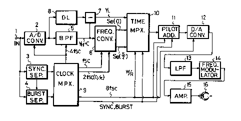
Fig. 1 is a systematic block diagram showing an
embodiment of a transmission system ~recording system~ of the
apparatus using a color television signal transmitting system
according to this invention;
Figs. 2A to 2E are respectively frequency spectrum
diagrams useful for explaining this invention;
Figs. 3A to 3D are respectively waveform diagrams
useful for explaining the present invention;
Fig. 4 is a waveform diagram showing an analog
signal that is used in the present invention; and
Fig. 5 is a systematic block diagram showing an
embodiment of a receiving system ~reproducing systeml of the
apparatus using the color television signal transmitting
system according to this invention.
(~
~;~749()7
DESCRIPTION OF THE PREFERRED EMBODIMENT
Now, an embodiment of an apparatus for recording
and reproducing a video signal on a recording medium using
a color television signal transmitting system according to
the present invention will hereinafter be described in detail
with reference to Figs. l to 5. In this case, this invention
is applied to a video tape recorder (VTR).
Fig. 1 schematically illustrates an example of a
recording system of the VTR to which this invention is applied~
In Fig. 1, a composite color video signal of, for example,
NTSC ~national television systems committee) is applied to
an input terminal 1 and then commonly supplied to an A/D
(analog-to-digital) converter 2, a synchronizing signal .
soparatin~ circuit 3 and a burst signal separating circuit 4.
The frequency spectrum of this composite color video signal
consists of, as shown in Fig. 2A, a frequency band of a
luminance signal Y of 0 to 4.2 MHz and a frequency band o~
a carrier chrominance signal e of + L.5 MHz-~ with 3.58 MHz as
the center. Reference numeral 5 designates a digital band-pass
filter (hereinafter simply referred to as BPF) and reference
numeral 6 designates a frequency converter. The output of
the A/D converter 2 is supplied to the BPF 5 and the output
of the BPF 5 is in turn supplied to the frequency converter
6 and a subtracter 7. Supplied to the subtracter 7 is the
output of the A/D converter 2 that is delayed by an appropriate
delay time by a delay line 8 and in the subtracter 7, the
output of the ~PF 5 is subtracted from the delayed output
supplied thereto as above. Reference numeral 9 designates a
clock signal generator to which a synchronizing pul~e and a
~;~74907
burst signal with color subcarrier frequency fSC are
respec~ively supplied from the synchronizing signal separat-
ing circuit 3 and the burst signal separating circuit 4.
On the basis of this burst signal, from the color signal
generator 9 there are produced a clock signal with frequency
of, for example, 4 fsc~ which then is fed to the A/D converter
2 and the BPF 5 and, a two-phase signal with frequency of,
for example, 2 fSC and then phase of which is 0 (zero) and ~
and a pulse with frequency fSC which are both supplied to the
frequency converter 6.
Reference numeral lO designates a time-compressing
multiplexer to which a pair of outputs from the frequency
converter 6, the output from the subtracter 7 and the clock 3
signal with the frequency of, for example, 8 fSC from the~
clock signal generator 9 are respectively supplied. Reference
numeral 11 designates a pilot signal adding circuit to which
the output from the time-compressing multiplexer 10 and the
pilot signal (formed of the synchronizing signal.and the
burst signal) from the clock signal generator 9 are respec-
tively supplied. The output of the pilot signal adding circuit
11 is sequentially supplied through a D/A (digital-to-analog)
converter 12 ~ and a low-pass filter 13 to an FM-modula--
tor 14. The output of the FM-modulator 14 is supplied through
a recording amplifier 15 to a magnetic recording head (rotary
magnetic head) 16 and then recorded on a recording medium
(not shown).
The operation of the recording system shown in ~ig.
1 will be now described. A high frequency band signal SH
that is the output of the BPF 5 is a digital signal correspond-
ing to the high frequency component YH of the luminance
~74907
signal Y and the chromaticity signal (carrier chrominance
signal) C, and the equivalent frequency spectrum thereof is
as shown in Fig. 2C. For simplicity, term,frequency, waveform
and so on of the original analog signal are used for those
of the transmission signal in the digital signal period,
hereinafter. Since the output of the BPF 5 is subtracted
from the output of the A/D converter 2, namely, the digital
composite signal Y + C in the subtracter 7, the output of
the subtracter 7 becomes a low frequency component YL of the
digital luminance signal Y and the frequency spectrum thereof
becomes as shown in Fig. 2B.
The output of the BPF 5 is frequency-converted to
the base band of a low frequency with the frequency fSC as
the center in the frequency converter 6 and the frequency
spectrum thereof becomes as shown in Fig. 2D. More particu-
larly, the waveform of the output SH (= YH + C) from the BPF
5 is, for example, as shown by a solid line in Fig. 3A.
This output signal is sampled in the frequency converter 6 by
two-phase signals with repetitive frequency 2 fsc and phases
of 0 and Tr as shown in Figs. 3C and 3D to thereby produce a
two-phase high frequency band luminance signal SH(0) that
consists of a zero-phase high frequency band luminance signal
YH2(0) and a zero-phase chrominance signal C2(0) obtained by
the sampling of the zero-phase signal and a signal SH(Tr/2)
that consists of a Tr-phase high frequency band luminance
signal YH2(~/2) and a Tr-phase chrominance signal C2(Tr/2)
obtained by the sampling of the TT-phase signal. As is clear
from Fig. 3, between the two-phase signals there is a phase
difference of TT radian and this phase difference corresponds
to the phase difference of TT/2 radian in the frequency fsc~
1 2749~)7
In the NTSC system, since the color subcarrier signal is
orthogonal two-phase amplitude-modulated by two chrominance
signals, if one of the sampling points by the above two-phase
signals is selected to be a zero-cross point of the subcarrier
signal in the original composite signal, the zero-phase
chrominance signal C2(0) and the ~-phase chrominance signal
C2(~/2) provided by the two-phase sampling respectively
become to correspond to color difference components (R - Y)
and (B - Y) of the original composite signal.
Since the repetitive frequency of the above zero-
phase signal and the ~-phase signal is 2 fsc~ in the frequency
spectrum of the two-phase high frequency band signals
- SH(0) = YH2(0) + C2(0) and that of SH(~/2) = YH2(~/2) ~ C2(~/2) 9
the center frequency thereof becomes the difference between
the sampling frequency 2 fSC and the center frequency fSC f
YH ~ C, namely, the frequency fsc~
In order to shift such two-phase high frequency band
signals SH(0) and SH(~/2) to the base band signals, the
following technique is employed in this embodiment.
~hat is, during the period in which the pulse having,
the repetitive frequency fSC and a pulse duty factor of 50% ,
as shown in Fig. 3B, which is supplied from the clock signal
generator 9 to the frequency converter 6, is at low level,
the respective sampling values (shown by black circ-les and
black triangles in Fig. 3A) by the zero-phase signal and the
~-phase signal are inverted in code (as shown by white circles
and white triangles in the same figure). The code inversion
at the repetitive frequency fSC is equivalent to the sampling
by the frequency fSC is so that the above two-phase high
frequency band signals SH(0) and SH(~/2) are respectively
~74~()7
converted to two-phase base band signals SB(O) = YH(O) + C(O)
and SB(~/2) = YH(~/2) + C(~/2) as shown by a broken line and
a one-dot chain line in Fig. 3A. At that time, the frequency
spectrum (Fig. 2C) of the high frequency band signal YH +~C
with the frequency fSC as its center is folded at a point of
zero frequency (Fig. 2D). The two-phase base band signals
SB(O) and SB(~/2) thus obtained contain no color subcarrier
wave and are equivalent to the component signal in this stand-
point.
If the high frequency band luminance signals YHA and
YHB are taken as a cos ~YHA~ and a cos ~YHBt (~YHA < ~SC ~YHB)
and the two-phase signals whose frequency-converting frequency
is fSC are taken as cos ~Sct and sin ~Sct, the base band
g s YHA(O), YHB(O), YHA(~/2) and YHB(~/2) are respectively
15' expressed as by the following equations (1) to (4).
YHA(O) = a cos ~yHAt cos ~Sct
= -~- {cos (~YHA + ~SC) t ~ cos (~YHA -- ~SC) t}
, a cos (~YHA ~SC) 0OOO (1)
YHB(0) ) - ~ - C08 (~YHB ~SC)t 0.OO (2)
YHA(~/2) = a cos ~YHA t sin ~Sct
= _~- {sin (~YHA + ~SC) t + 8in(~YHA Ysc)9 }
_~_ sin (~YHA ~SC)
yHB(~/2) ~ _~- sin (~YHB ~ ~SC~ ............... r o t4)
where the sum frequency component is removed by the low-pass
filter 13.
When the folded spectrum of the high frequency band
luminance signal YHB is overlapped on the spectrum of the high
frequency band luminance signal YHA, the following equation t5)
-- 10 --
1~74907
is established.
~YHA ~SC ( ~YHB ~SC) ~ ~5)
Substituting the equation (5) into the equations
(l) to (4) yields
YHA(O) + YHB(O) = -~- {cos ~t + cos (-w~) t }
= a cos ~t oo-- (6)
HA(~/2) + YHB(~/2)
= -2a {sin ~ + sin (-~) t }
=
The two-phase base band signals SB(0) and S~(~/2)
from the frequency converter 6 and the signal YL from the
subtracter 7 are supplied to the time-compressing multiplexer
10 and then written in a RAM (random access memory), that is
incorporated in the multiplexer 10 under such address control
that on the basis of the clock signal with the repetitive
frequency of 8 fsc~ the first data of the line thereof
becomes the 0-address of the RAM. As mentioned before~ since
the sampling frequency in the A/D converter 2 and the BPF S
is 4 fsc~ the sampling frequency of the signal YL that is the
difference signal between the both outputs i8 also ~ fsco
As a result, in the time-compressing multiplexer lO, the low
frequency band luminance signal YL is time-compressed with a
time-compressing ratio 2(= 8 fSC . 4 fSC) to
time-compressed low frequency band luminance signal YLC and
the frequency spectrum of this signal YLC is enlarged twice
that of the low frequency band luminance signal YL that is
as shown in Fig. 2B. Further, since the sampling frequency
of the two-phase base band signals SB(0) and SB(~/2) is 2 fSC
in the time-compressing multiplexer 10, the above two-phase
-- 11 --
~74907
base band signals are respectively time-compressed with ~
time-compressing ratio 4 (= 8 fsc . 2 fsc) to become a pair
of time-compressed base band signals sBc(o) = YHc(o) + cc(o)
and SBC (~/2) = YHC (~/2) + CC (~/2) . Accordingly, the frequency
spectrum of the both time-compressed base band signals is
enlarged four times that of the signal shown in Fig. 2D.
The time-compressed low frequency band luminance signals and
the time-compressed base band signals thus made are respectively
read out from the RAM by known read control means on the
basis of the clock signal of 8 fSC in such a manner that
they may be inserted into one horizontal period (lH). In this
case, since the frequency band of each signal after being
time-compressed is made the same, it is possible to use the
transmission line efficiently.
The output signal from the time-compressing multi-
plexer lO i~ supplied to and added with a pilot signal (con-
sisting of the synchronizing signal and the burst signal)
indicative of the sampled phase of the incoming composite color
video signal in the pilot signal adding circuit ll. Thereafter,
it is reconvered to the analog signal by the D/A converter 12.
This analog signal is a time-compressed serial color signal
(hereinafter simply referred to as a time-compressed serial
signal) that consists of, as shown in Fig. 4, the horizontal
synchronizing signal, the burst signal, the time~compressed
low frequency band luminance signal YLC the time base of
which is compressed to l/2 and the both time-compressed base
band signals SBc(O) and SBc(~/2) whose time bases are compress-
ed to l/4. Similarly to the prior art, this analog signal is
used to directly FM-modulate the carrier wave of the FM-modulator
14 and this FM-modulated signal is supplied through the recording
1274907
amplifier 15 of appropriate characteristic to the recording
head 16 to be recorded on the recording medium.
A reproducing system for reproducing the time-compress-
ed color television signal recorded as above will be described
with reference to Fig. 5.
In Fig. 5, reproduced output by a playback head 21
from a recording medium (not shown) is supplied through a
playback amplifier 22 to an FM-modulator 23. Reference
numerals 24 and 25 respectively designate a pilot signal
separating circuit and a clock signal generator. A pilot
signal separated from the output of the FM-demodulator 23
shown in Fig. 4 by the pilot signal separating circuit 2~ is
supplied to the clock signal generator 25. Reference numeral
26 designates an A/D converter and reference numeral 27
designates a memory. The A/D converter 26 is supplied with
the analog output of the FM-demodulator 23 and also with a
clock signal of frequency 8 fsc~ from the clock signal
generator 25. The digital output of the A/D converter 26 is
supplied to the memory 27. Reference numeral 28 designates
a memory control circuit and reference numeral 29 designates
a signal generator. The memory control circuit 28 is supplied
with the output signal of frequency 8 fsc~ from the clock
signal generator 25 and the output of frequency,8 fSC from
the signal generator 29 which is generated on the basis of
a reference signal REF applied thereto through an input
terminal 30. Then, the control signal is supplied from the
control circuit 28 to the memory 27.
Reference numeral 31 designates a multiplexing
separating and time- expander ~hereinafter simply referred to
as separating/time-expander) and reference numeral 32 designates
- 13 -
~74907
a frequency converter. The separating/time-e~pander 31 is
supplied with the time-compressed serial signal that is read
out from the memory 27 and the output from the signal generator
29. The frequency converter 32 is supplied with a pair of
two-phase base band signals from the separating/time-expander
31, the two-phase signals of frequency 2 fSC and the signal
with frequency fSC both from the signal generator 29. The
low frequency band luminance signal that is another output
of the separating/time-expander 31 and the output of the
frequency converter 32 are supplied to ani,adder 33. The
digital output from the adder 33 and the clock signal with
frequency 4 fSC from the signal generator 29 are supplied to
a D/A converter 34. Reference numeral 36 designates a
processor which is supplied with the analog output of the
D/A converter 39 through a low-pass filter 35 and the synchro-
nizing signal and the burst signal from the signal generator
29. The output from the processor 36 is delivered to an
output terminal 37.
The operation of the reproducing system as shown in
Fig. 5 will be described. The pilot signal ( consisting of
the synchronizing signal and the burst signal) that is
separated by the pilot signal separating circuit 24 indicates
the sampling phase of the recording system as mentioned before
in connection of Fig. l. This pilot signal is affected by
the jitter caused by the tape transporting system ~f the ~TR
and hence contains an time base error. Then, the clock signal
with frequency 8 fsc~ {= 8 fSC + ~f(t)} that is produced by
the clock signal generator 25 which is supplied with this
pilot signal is accurately locked to the sampling phase upon
the recording mode. On the basis of this clock signal, the
- 14 -
~749(~7
analog output of the FM-demodulator 23, namely, the time~
compressed serial signal is A/D-converted by the A/D converter
26 and the output of the A/D converter 26 is written in the
memory 27 that forms a time base corrector whiIe controlling
its address by the memo~y control circuit 28. The content
or data stored in the memory 27 is sequentially rea~ out
therefrom on the basis of the clock signal with very stable
frequency 8 fSC that is supplied thereto through the control
circuit 28 from the signal generator 29. As a result, ~he
jitter of the ~TR is absorbed at this stage.
The separating/time-expander 31 includes the RAM
and the time-compressed serial signal that is read out in
turn from the memory 27 is sequentially written in the RAM
of the separating/time-expander 31 on the basis of the clock
signal with frequency 8 fSC from the signal generator 29.
Of the time-compressed serial signal written in the RAM, the
time-compressed low frequency band luminance signal YLC is
sequantially read out from the RAM on the basis of the clock
signal with frequency 4 fSC from the signal generator 290
In this case, since the time-expanding ratio is 2 (= 8 fSC -
4 fsc)~ at this stage, the time-compressed low frequency band
luminance signal YLC is restored to the low frequency band
luminance signal YL. On the other hand, the zero-phase and
~-phase time-compressed base band signals SBc(O~ and SBc(~/2)
are read out from the ~AM in parallel on the basis of the
clock signal with frequency 4 fSC from the signal generator 290
In this case, the time-expanding ratio of each time-compressed
base band signal is 2 ~= 8 fSC 4 fSC) and hence at this staget
each time-compressed base band signal is yet in the half
time-expanded state. The half time-expanded base band signals
1~ 7 4 ~7
SB~ (O) and SB'(~/2) from the separating/time-expander 31 are
respectively supplied to the frequency-converter 32 and then
sampled by the zero-phase and ~-phase sampling signals of
frequency 2 fSC that are supplied from the signal generator
29. In the stage of this two-phase sampling operation, each
of the half time-expande~ base band signals is again time-
expanded with the time-expanding ratio 2 and frequency-converted
so as to restore the two-phase high frequency band signals
SH(0 ? and SH(~/2~. Since the frequency spectrum of the two~
phase high frequency band signal is centered at 2 fsc~
similarly to the frequency-converter 6 in the recording
apparatus, the two-phase high frequency band signal is again
frequency-converted in the frequency converter 32 by the pulse
signal with frequency fSC supplied thereto from the signal
generator 29, thus the original high frequency band signal
YH + C being pr~duced.. This high frequency band signal YH ~ C
and the low frequency band luminance signal YL from the
separating/time-expander 31 are added together in the adder
33 and then converted to the analog video signal by the D/A
converter 34. This analog video signal is supplied through
the low-pass filter 35 to the processor 36, in which it is
added with the synchronizing signal and the burst signal from
the signal generator 29 to become the original composite color
video signal, which then is delivered to the output terminal
37.
When the high frequency band luminance signal
component and the carrier chrominance signal component (YH + C~
are frequency-converted and re-converted in the form of the
analog signal, it is extremely difficult to completely match
the characteristics of the separation filter for the signal
- 16 -
~749()7
component (YH + C), the low-pass filter after being converted
to the base band, and the band-pass filter after being re-con-
verted upon playback, level of each signal, group delay chara-
cteristic, phase of the frequency-converted signal and the
like and to maintain them.
In accordance with this invention, since the signal
processings of the signal component (YH + C) are all carried
out in the form of the digital signal, theEe is no defect in
the case of the signal processing in the form of the analog
signal and so, the signal transmission of high quality becomes
possible.
If the high frequency band luminance signals YHA2(0)~
YHB2(~2) and YHB2(~/2) in the respective phases that are
frequency-converted from the base band in the frequency-converter
32 are expressed by numerical formula, they become as shown
by the following equations (8) to ~11).
HA2¦0) = YHA(O) cos (~)Sct
z a cos (~YHA ~ ~SC) t cos ~SCt
= _~- {cos ~yHAt + cos (~YHA 2~SC) t}
y (0) = -~- cos ~yHBt + cos (~YHB - SC
HA2(~/2) = YHA(~/2) sin ~sct
= -a sin (~YHA - ~SC) t sin ~SCt
~:25 = _~- {cos ~yHAt - cos (~YHA 2~SC)
YHB2`(~/2) = -~- { ~YHBt COs (~YHB ~ 2~SC) t}ooO (11)
Each second term of the eq~ations (8) to (11) is an
unnecessary component. As ~YH comes close to ~SC' each
frequency of the unnecessary component becomes close bo ~SC
and becomes unable to be separated by the ordinary filter.
- 17 -
~ 7 4 9~
However, according to this embodlment, when the high frequency
band luminance signal YH is obtained by the frequency converter
32, the unnecessary component can be cancelled out. The
unnecessary component of the carrier chrominance signal C can
be cancelled out perfectly similarly.
When the folded spectrum of the high frequency band
luminance signal YHB is again frequency-converted, the follow-
ing equation (12) is established.
,, {YHA~O) + YHB()} COs Sct
= a cos ~t cos ~Sct
~ {cos ~Q ~ ~SC) t + cos (~ + ~SC) t}
= a {cos (~YH ~ 2~sc~t I cos ~YH } ~O~ (12)
( YHB ~SC) is established, the
1~ first ~tem of the equation (12) is cancelled out as set
forth above. However~ in the case of the folded spectrum,
the afore-noted equation (7) becomes zero so that the first
item remains as it is and ~YHB component is reproduced.
While in the above embodiment, the time-compressed
low frequency band luminance signal and the both time-compressed
base band signals are time-compressed so as to be inserted
into the 1 H period and then transmitted through one trans-
mission channel, they can be transmitted through two trans-
mission channels. That is, it is possible that the low
frequency band luminance signal is not time-compressed and
then transmitted through one transmission channel but the
both base band signals are time-compressed with time-compress-
ing ratio 2 so as to be inserted into the lH period and then
transmitted through other one channel. In this case, it is
possible that a necessary frequency band of the transmitting
4g()7
apparatus is narrow as compared with that of the transmissior
of the original signal.
As set forth above, according to this invention,
the frequency-conversion of the two-phase sampling frequencies
is employed to remove the influence of the color subcarrier
wave and the time-compressed serial color signal that corre-
sponds to the transmission of the component video signal is
obtained and hence the signal transmission of high quality
becomes possible.
The above description is given on a single preferred
embodiment of the invention, but it will be apparent that many
modifications and variations could be effected by one skilled
in the art without departing from the spirits or scope of the
novel concepts of the invention, so that the scope of the
invention should be determined by the appended claims only. -
-- 19 --