Sélection de la langue

Search

Sommaire du brevet 1276685 

Énoncé de désistement de responsabilité concernant l'information provenant de tiers

Une partie des informations de ce site Web a été fournie par des sources externes. Le gouvernement du Canada n'assume aucune responsabilité concernant la précision, l'actualité ou la fiabilité des informations fournies par les sources externes. Les utilisateurs qui désirent employer cette information devraient consulter directement la source des informations. Le contenu fourni par les sources externes n'est pas assujetti aux exigences sur les langues officielles, la protection des renseignements personnels et l'accessibilité.

Disponibilité de l'Abrégé et des Revendications

L'apparition de différences dans le texte et l'image des Revendications et de l'Abrégé dépend du moment auquel le document est publié. Les textes des Revendications et de l'Abrégé sont affichés :

  • lorsque la demande peut être examinée par le public;
  • lorsque le brevet est émis (délivrance).
(12) Brevet: (11) CA 1276685
(21) Numéro de la demande: 1276685
(54) Titre français: EMETTEUR-RECEPTEUR RADIO COMPORTANT UN CIRCUIT DE COMMUTATION D'ANTENNE POUVANT CHANGER LA SENSIBILITE DE RECEPTION
(54) Titre anglais: RADIO TRANSCEIVER INCLUDING AN ANTENNA SWITCHING CIRCUIT CAPABLE OF CHANGING RECEPTION SENSITIVITY
Statut: Périmé et au-delà du délai pour l’annulation
Données bibliographiques
(51) Classification internationale des brevets (CIB):
  • H04B 01/44 (2006.01)
  • H04B 01/10 (2006.01)
(72) Inventeurs :
  • UEDA, HIDEKI (Japon)
  • BABANO, SOTOAKI (Japon)
(73) Titulaires :
  • NEC CORPORATION
(71) Demandeurs :
  • NEC CORPORATION (Japon)
(74) Agent: SMART & BIGGAR LP
(74) Co-agent:
(45) Délivré: 1990-11-20
(22) Date de dépôt: 1987-04-08
Licence disponible: S.O.
Cédé au domaine public: S.O.
(25) Langue des documents déposés: Anglais

Traité de coopération en matière de brevets (PCT): Non

(30) Données de priorité de la demande:
Numéro de la demande Pays / territoire Date
80138/1986 (Japon) 1986-04-09

Abrégés

Abrégé anglais


ABSTRACT
A radio transceiver includes an antenna, a transmitter,
a receiver and an antenna switching circuit for selectively coupl-
ing the transmitter and the receiver to the antenna in response
to a transmit mode and a receive mode. The antenna switching
circuit includes a first diode coupled between the antenna and the
transmitter, a second diode and an inductor connected in series
between a point of fixed potential and the junction of the antenna
and the first diode. The receiver is coupled to the junction of
the second diode and the inductor. According to the invention,
the resistances of the first and second diodes are changed in
response to another receive mode to reduce the level of a received
signal supplied to the receiver. The invention reduces inter-
ference and improves temperature stability.

Revendications

Note : Les revendications sont présentées dans la langue officielle dans laquelle elles ont été soumises.


66446-428
THE EMBODIMENTS OF THE INVENTION IN WHICH AN EXCLUSIVE
PROPERTY OR PRIVILEGE IS CLAIMED ARE DEFINED AS FOLLOWS:
1. A radio transceiver comprising an antenna, a
transmitter, a receiver, an antenna switching circuit including
switching diodes for coupling said transmitter and said receiver
to said antenna in response to a transmit mode and a receive mode,
respectively, and means for changing the resistances of said
switching diodes in response to another receive mode to reduce the
level of a received signal supplied from said antenna to said
receiver.
2. A radio transceiver comprising an antenna, a
transmitter, a receiver and an antenna switching circuit including
first and second switching diodes, first means for giving a high
resistance to said switching diodes by providing a first bias to
said switching diodes in a receive mode to couple said antenna to
said receiver, second means for giving a low resistance to said
switching diodes by providing a second bias to said switching
diodes in a transmit mode to couple said transmitter to said
antenna, and third means for giving a resistance lying between
said high and low resistances to said switching diodes by
providing a third bias to said switching diodes in another receive
mode.
3. A radio transceiver as claimed in claim 2, comprising
means for selecting one of said first and third means in response

66446-428
to a control signal.
4. A radio transceiver as claimed in claim 3, wherein said
control signal comprises a signal representative of the intensity
of a radio signal received in one of said receive modes.
5. A radio transceiver as claimed in claim 3, comprising
key board means for generating said control signal.
6. A radio transceiver as claimed in claim 2, comprising
means for varying the output level of said transmitter in response
to a control signal.
7. A radio transceiver as claimed in claim 6, comprising
key board means for generating said control signal.
8. A radio transceiver as claimed in claim 6, comprising
means for selecting one of said first and third means in response
to another control signal representative of the intensity of a
received radio signal.
9. A radio transceiver including: an antenna, a
transmitter, a receiver, and an antenna switching circuit for
selectively coupling said transmitter and said receiver to said
antenna in response to a transmit mode and a receive mode,
respectively, the antenna switching circuit including: a first
diode coupled between said antenna and said transmitter, a second

66446-428
diode and an inductor connected in series between a point of fixed
potential and the junction of said antenna and said first diode,
and means for coupling said receiver to the junction of said
second diode and said inductor, and means for changing the
resistances of said first and second diodes in response to a
control signal to couple said antenna to said transmitter in a
transmit mode, to couple said antenna to said receiver in first
and second receive modes, a received signal being supplied from
said antenna to said receiver in said first receive mode, and a
received signal having a reduced level being supplied to said
receiver in said second receive mode.
10. A radio transceiver comprising: an antenna; a
transmitter; a receiver; an antenna switching circuit for
selectively coupling said transmitter and said receiver to said
antenna in response to a transmit mode and a receive mode,
respectively; first switching means for connecting said antenna
switching circuit to one of a first, second and third potential,
said first potential for causing said antenna switching circuit to
selectively couple said antenna to said receiver such that a
received signal can be applied to said receiver in a first receive
mode, said second potential for causing said antenna switching
circuit to selectively couple said antenna to said receiver such
that a received signal of reduced level can be applied to said
receiver in a second receive mode, and said third potential for
causing said antenna switching circuit to selectively couple said
antenna to said transceiver in a transmit mode.

66445-428
11. A radio transceiver as claimed in claim 10, wherein said
transmitter produces one of a plurality of transmission signals of
a plurality of levels in response to a control signal.
11

Description

Note : Les descriptions sont présentées dans la langue officielle dans laquelle elles ont été soumises.


~;2'76685
RADIO TRANSCEIVER INCLUDING ~N
ANTENNA SWITCHING CIRCUIT CAPABLE
OF CHANGING RECEPTION SENSITIVITY
Background of the Invention
The present invention relates to a radio transceiver
including an antenna switching circuit and, more
particularly, to an antenna switching circuit capable of
chan~ing reception sensitivity.
In a radio transceiver of the type described, it has
been customary to selectively connect a transmitter and
a receiver to an antenna by an antenna switching circuit
which is responsive to a transmission/receipt control
signal and comprised of diodes and others, thereby
transmitting or receiving such a radio signal as a
frequency modulated signal. Such a transceiver is
proposed in the European Patent Publication A2-0151014
published in July 8, 1985 and assigned to MEC Corporation.
A prerequisite with a radio transceiver having the
above construction is that two remote transceivers, which
are in communication, are free from the interference of
alien signals. An implementation heretofore adopted to
meet such a requisite is varying the gain and, thereby,
the reception sensitivity by changing the current value
(e.g. emitter current value) of a transistor which is
installed in the receiver for high frequency amplification
(RF AMP).

1~7~685
~- 2 -
However, such a prior art implementation suffers
from a drawback that when the current of the transistor
for RF AMP is reduced, the transceiver becomes susceptible
to mutual interference and, in addition, the decrease in
the bias emitter current may deteriorate the temperature
characteristic.
Summary of the Invention
It is therefore an object of the present invention
to provide a radio transmitter including an antenna
switching circuit which is free from the above-described
drawback.
The present invention is applicable to a radio
transceiver having an antenna, a transmitter, a receiver
and an antenna switching circuit including switching
diodes for coupling the transmitter and the receiver to
the antenna in response to a transmit mode and a receive
mode, respectively. The present transceiver includes
means for changing the resistances of the switching diodes
in response to another receive mode to reduce the level of
a received signal supplied from the antenna to the receiver.
Brief Description of the Drawings
The above and other objects, features and advantages
of the present invention will become more apparent from
the following detailed description taken with the
accompanying drawing in which:

lZ~7668S
-- 3 --
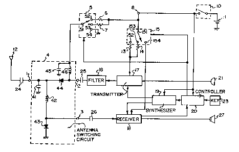
Fig. 1 is a circuit diagram showing a radio
transceiver including an antenna switching circuit in
accordance with the present invention.
Detailed Description of the Invention
Referring to Fig~ 1, when a power switch 10 is
closed, DC power voltage is applied from a battery 11 to
a synthesizer 19 and a controller 20. The controller 20
in turn delivers a channel designation signal to the
synthesizer 19 to set up a transmission/receipt frequency.
In a transmit mode operation, the controller 20 so
controls switches 15 and 5 as to route the DC power voltage
to a transmitter 17 and an antenna switching circuit 4 and
not to a receiver 18. Specifically, during transmission,
the switch 5 is controlled to connect terminals 51 and 52
thereof. A resistor 6 has resistance R6 which is smaller
than the resistance R7 of a resistor 7 so that, under the
above condition, the greatest current flows through diodes
43 and 44 to render them fully conductive. Consequently,
an antenna terminal 1 and a transmitter terminal 2 are
interconnected while, at the same time, a capacitor 41 and
a coil 42 complete a parallel resonance circuit for
transmit frequency. Nence, the transmitter terminal 2 and
~' a receiver terminal 3 are broughtinto an open condition,
and so are the antenna terminal 1 and the receiver
terminal 3.

~Z~66~15
-- 4 --
In the above condition, voice entered via a micro-
phone 21 is modulated, frequency-converted and amplified
by the transmitter 17 and, then, fed to an antenna 12 via
a filter 16, a capacitor 25, a diode 44 and a capacitor 24
to be transmitted to a remote transceiver. In the transmit
mode, the switch 15 is controlled by the controller 20 to
connect its terminal 151 to a terminal 152 or a terminal
153. If the resistance of a resistor 13 is selected to be
smaller than that of a resistor 14l the transmission output
of the transmitter 17 becomes greater when the terminal 151
is connected to the terminal 152 than when it is connected
to the terminal 153.
In a receive mode operation, on the other hand, the
controller 20 controls the switch 15 such that the DC
power voltage is applied to the receiver 18 and not to
the transmitter 17. Namely, it connects the terminal 151
of the switch 15 to a terminall54. Also controlled by the
controller 20, the switch 5 connects its terminal 51 to a
terminal 53 or a terminal 54. When the terminals 51 and 53
are interconnected in a first receive mode, the current
flowing through the diodes 43 and 44 is smaller than the
current which flows in the transmit mode because the
resistance R6 is smaller than the resistance R7, as
previously stated. As a result, the operating resistance
of the diode 43 increases relatively and, hence, the
coupling between the antenna terminal 1 and the receiver
terminal 3 is intensified in proportion to the operating

127~ 35
-- 5
resistance of the diode 43. It follows that any desired
amount of coupling may be set up between the antenna
terminal 1 and the receiver terminal 3 by suitably
selecting the resistance R7 of the resistor 7. In this
instance, the influence of the diode 44 is negligible.
This is because, in a receive mode in which the transmitter
17 is OFF, the impedance on the transmitter side as viewed
from the terminal 2 side can be increased by adequately
selecting the distance of connection (electrical length)
from the terminal 2 to the transmitter 17, to such a degree
that the in~luence of the transmitter side is negligibleu
On the other hand, when the terminals 51 and 54 are
connected in a second receive mode, current does not flow
through the diodes 43 and 44 to equivalently set up an open
condition and, therefore, the amount of coupling between
the antenna terminal 1 and the receiver terminal 3 can be
made greatest.
It is to be noted that the current changeover by the
switch 5 has been shown and described as occurring in
three steps, four or more changeover steps may be ~dopted
to change the amount of coupling more minutely.
The control over the switches 5 and 15 is performed
as follows.
A signal coming in through the antenna 12 is fed to
the receiver 18 via an antenna switching circuit 4. The
receiver 18 delivers to the controller 20 a signal which
is representative of the intensity of the received signal.

~Z~76685
-- 6
When the intensity of the received signal is greater than
a predetermined reference level, the controller 20 controls
the switch 5 to connect the texminal 51 to the terminal 53
to reduce the above-mentioned amount of coupling and,
thereby, the reception sensitivity. In a transmit mode
following such a receive mode, the controller 20 may
control the switch 15 to connect the terminal 151 to the
terminal 153 in order to lower the transmission output
level.
In the embodiment shown and described, the reception
sensitivity and the transmission output are automatically
varied by equivalently approximating the distance between
the own station and a remote station based on the intensity
of a received signal. In an alternative embodiment, a key
board 23, which is connected to the controller 20, may be
operated to manually vary the reception sensitivity as
well as the transmission output level. Further, an
arrangement may be made such that a control signal which
comes in over a control channel from a remote transceiver
is received by the receiver 18 while, in response to the
received control signal information, the controller 20 is
operated to control the switches 5 and 15.
In summary, it will be seen that a radio transceiver
including an antenna switching circuit of the present
invention is capable of surely changing reception
sensitivity with a minimum number of structural elements.
This unprecedented advantage is deri.ed from means whicb

~'~66~35
is capable of varying the current flowing through antenna
switching diodes in three or more steps. Specifically,
the transceivex with such means changes over two or more
current values in a receive mode and, thereby, changes
the amount of coupling without resorting to a transistor
for RF AMP.

Dessin représentatif
Une figure unique qui représente un dessin illustrant l'invention.
États administratifs

2024-08-01 : Dans le cadre de la transition vers les Brevets de nouvelle génération (BNG), la base de données sur les brevets canadiens (BDBC) contient désormais un Historique d'événement plus détaillé, qui reproduit le Journal des événements de notre nouvelle solution interne.

Veuillez noter que les événements débutant par « Inactive : » se réfèrent à des événements qui ne sont plus utilisés dans notre nouvelle solution interne.

Pour une meilleure compréhension de l'état de la demande ou brevet qui figure sur cette page, la rubrique Mise en garde , et les descriptions de Brevet , Historique d'événement , Taxes périodiques et Historique des paiements devraient être consultées.

Historique d'événement

Description Date
Inactive : CIB de MCD 2006-03-11
Le délai pour l'annulation est expiré 2002-11-20
Lettre envoyée 2001-11-20
Accordé par délivrance 1990-11-20

Historique d'abandonnement

Il n'y a pas d'historique d'abandonnement

Historique des taxes

Type de taxes Anniversaire Échéance Date payée
TM (catégorie 1, 7e anniv.) - générale 1997-11-20 1997-10-21
TM (catégorie 1, 8e anniv.) - générale 1998-11-20 1998-10-22
TM (catégorie 1, 9e anniv.) - générale 1999-11-22 1999-10-18
TM (catégorie 1, 10e anniv.) - générale 2000-11-20 2000-10-20
Titulaires au dossier

Les titulaires actuels et antérieures au dossier sont affichés en ordre alphabétique.

Titulaires actuels au dossier
NEC CORPORATION
Titulaires antérieures au dossier
HIDEKI UEDA
SOTOAKI BABANO
Les propriétaires antérieurs qui ne figurent pas dans la liste des « Propriétaires au dossier » apparaîtront dans d'autres documents au dossier.
Documents

Pour visionner les fichiers sélectionnés, entrer le code reCAPTCHA :


Pour visualiser une image, cliquer sur un lien dans la colonne description du document. Pour télécharger l'image (les images), cliquer l'une ou plusieurs cases à cocher dans la première colonne et ensuite cliquer sur le bouton "Télécharger sélection en format PDF (archive Zip)" ou le bouton "Télécharger sélection (en un fichier PDF fusionné)".

Liste des documents de brevet publiés et non publiés sur la BDBC .

Si vous avez des difficultés à accéder au contenu, veuillez communiquer avec le Centre de services à la clientèle au 1-866-997-1936, ou envoyer un courriel au Centre de service à la clientèle de l'OPIC.


Description du
Document 
Date
(aaaa-mm-jj) 
Nombre de pages   Taille de l'image (Ko) 
Abrégé 1993-10-13 1 19
Revendications 1993-10-13 4 96
Dessins 1993-10-13 1 19
Description 1993-10-13 7 197
Dessin représentatif 2001-09-20 1 12
Avis concernant la taxe de maintien 2001-12-17 1 178
Taxes 1996-10-15 1 81
Taxes 1995-10-15 1 79
Taxes 1994-10-23 1 74
Taxes 1993-10-17 1 42
Taxes 1992-10-18 1 25