Note : Les descriptions sont présentées dans la langue officielle dans laquelle elles ont été soumises.
B26769310
~6~ 4
1 ~ELDING TRANSFORMER AND
RECTIFIER ASSEMBLY
BACKGROUND OF THE INVENTION
_
The present invention relates to welding
transformers and rectifiers, and more particularly to
transformers and rectifiers for robotic welders.
In resistance welding, coalescence is produced
primarily by resistive heat created by passing an electric
current through the workpiece. A resistance welder
includes primary conductors, a transformer, secondary
conductors, and welding electrodes. The primary
conductors couple the transformer to a power source. The
secondary conductors interconnect the transformer and the
electrodes.
Typically, the primary power source or supply in
resistance welding provides power at the line
frequency--for e~ample, 60 hertz ~Hz) in the United States
and 50 EIz in Europe. Welding transformers for this
relatively low-frequency current are excessively heavy for
many robotic welders where weight is a primary
consideration.
In an attempt to reduce the weight of the
transformer, artisans have used relatively high-frequency
power sources (e.g., 400 or 1200 E~z). By so boosting the
frequency, the transformer weight can be greatly reduced.
However, the increased frequency requires the secondary
voltage to be increased because of increased inductive
reactance, which is directly proportional to frequency.
In an attempt to reduce impedance, artisans have rectified
the secondary voltage/current. One such construction is
illustrated in United States Reissue Patent 31,444,
--1--
~'~76~374
1 reissued November 15, 1983, to Block, and entitled
TWO-PHASE TRANSFORMER AND WELDING CIRCUIT THEREFOR. Such
constructions are relatively bulky and heavy and therefore
not fully adaptable to all robotic welders. Further, the
shunts between the transformer and the rectifier are
"inductive throats~, such that the high-frequency
reactance prohlem remains.
SUMMARY OF THE INVENTION
The aforementioned problems are overcome in the
present invention wherein an extremely lightweight and
compact welding transformer and rectifier assembly
provides a rectified secondary current. The size and
weight of the unit are greatly reduced over known units;
and the unit is believed to comply with all known weight
and size restrictions for robotic welders.
In a first aspect of the invention, the rectifier
assembly directly abuts the secondary pads of the
transformer to eliminate inductive throats therebetween.
More particularly, in this aspect, the transformer
includes a pair of secondary pads, at least one diode
overlying and abutting each secondary pad, and a rectified
bus overlying and abutting the diodes. Consequently, a
rectified current is outputted on the rectified bus. The
sandwiching of the diodes directly against the secondaries
greatly reduces both the profile of the transformer and
its weight. Inductance due to electrical connections
between the transformer and the rectifier assembly are
virtually eliminated. The unit therefore provides
improved performance in a smaller and lighter weight
package than known units.
In a second aspect of the invention, the common
--2--
7697~
1 bus of the transformer is configured to further reduce the
size and weight of the unit. More particularlyl in this
aspect, the transformer includes a pair of coplanar
secondary pads, a planar common bus overlying the
secondary pads, and a plurality of secondary coil turns.
Each turn includes a first end connected to the common bus
and a second end extending through or beyond the common
bus and connected to one of the secondary pads.
Preferably, the bus defines some apertures permitting the
second turn ends to extend therethrough without
electrically contacting the bus. This intermeshing of the
coil turns and common bus further reduces the transformer
unit size and weight.
These and other objects, advantages, and features
of the invention will be more fully understood and
appreciated by reference to the detailed description of
the preferred embodiment and the drawings.
BRIEF DESCRIPTION OF THE DRAWINGS
~; Fig. 1 is a side plan view of the welding
transformer and rectifier assembly of the present
invention;
Fig. 2 is a top elevational view of the assembly;
FigO 3 is an end elevational view taken from the
right side of Fig. 2;
Fig. 4 is an end elevational view taken from the
~ left side of Fig. 2;
- Fig. 5 is a view taken along plane V-V in Fig. 2;
~,
Fig. 6 is a view taken along plane VI-VI in Fig.
2; and
Fig. 7 is an elevational view of the common bus.
,,
-3-
.
~76~ 7~
1 DETAILED DESCRIPTION OF THE PREFERRED EMBODIMENT
,
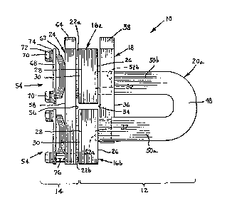
A welding transformer and rectifier unit or
assembly constructed in accordance with a preferred
embodiment of the invention is illustrated in the drawings
and generally designated 10. The transformer includes a
transformer portion 12 and a rectifier portion 14 (Eigs. 1
and 2). The transformer portion 12 includes a pair of
generally coplanar secondary connectors or pads 16a and
16b, a common bus 18, and a secondary coil 20. Each turn
of the coil 20 includes a first end electrically connected
to the common bus 18 and a second end electrically
connected to one of pads 16a and 16b. The common bus 18
is configured to permit the second end of each turn to
extend therethrough without electrically contacting the
bus. The rectifier portion 14 includes a plurality of
disk diodes 22a and 22b sandwiched against the secondary
pads 16a and 16b, respectively, and a rectified bus 24
sandwiched against the diodes 22. Alternating current on
the secondar~ pads 16 is rectified to single-phase DC
current on the rectified bus 24.
Each of the secondary pads 16 (Figs. 1-3 and 5)
is a generally rectangular parallelepiped. Each secondary
pad 16 includes a coil face 26 and an opposite rectifier
face 28. The coil faces 26 of the two pads are coplanar,
and the rectifier faces 28 are also coplanar and parallel
to the coil faces. Optionally, wear pads 30 can be
mounted on rectifier faces 28. If included, each wear pad
30 preferably extends the full height and width of the
secondary pad 16 on which it is mounted. The secondary
pads 16 define slots 32 in their coil faces 26 to receive
the coils 20. The pads also define tapped bores 33 to
-4-
6974
1 receive bolts 70 as will be described.
The common bus 18 (Figs. 1-3 and 7) is generally
planar and generally parallel to the secondary pads 16.
The common bus 18 includes a pad face 34 and a coil face
36, which are parallel to one another. The common bus 18
includes a terminal portion 38 defining tapped bores 40
which receive electrical connectors in conventional
fashionO The common bus 18 also defines a pair of
rectangular apertures or voids 42b and 42d (Fig. 7) which
extend through the common bus to receive certain coil ends
as will be described. Opposite terminal edge 38 are a
pair of arms 44a and 44b which define a void or open-sided
aperture 42c therebetween. A fourth void or open-sided
aperture 42d is located directly below arm 44a. A
plurality of slots or recesses 46a, 46b, 46c, and 46d are
formed in the coil face 36 of the common bus 18 to receive
coil ends.
The turns or loops of secondary coil 20 (Figs.
1-3) are generally identical to one another. The turns
are grouped into two sets of physically alternating turns
,~ or every other turn--a first set including turns 20a and
20c and a second set including turns 20b and 20d. Each of
the turns 20 is extruded copper and preferably hollow to
permit water cooling.
The turn 20a (Figs. 1 and 2) includes a bight
portion 48 and a pair of legs 50a and 50b extending
therefrom. The legs 50 are generally physically parallel
to one another, and leg 50a is longer than 50b. Leg 50a
includes a pad end 52a which extends through void 42a in
the common bus and is electrically connected to the
; secondary pad 16b. Leg 50a therefore does not contact the
~ -5-
~7~
1 common bus 18 but only the secondary pad 16b. The turn
end 52a is silver soldered in the slot 32 in the secondary
pad 16b~ The shorter leg 50b includes a bus end 52b
positioned ~ithin slot 46a of the common bus 18.
Consequently, leg 50b does not extend through the common
bus, but rather is electrically connected thereto.
Turn 20c is identical to turn 20a and includes a
longer leg 50a, which extends through void 42c in the
common bus 18 and is connected to pad 16b, and a shorter
leg 50b which is electrically connected to the common bus
in slot 46c. Consequently, the first set of turns 20a and
20c is electrically connected to the common bus 18 and to
the secondary pad 16b. The common bus 18 is configured to
receive the long legs 50a of turns 20a and 20c
therethrough.
Turns 20b and 20d (Figs. 2-3) are generally
identical to turns 20a and 20c but are rotated 180 degrees
or "flipped overn. Consequently, longer legs 50a of turns
20b and 20d extend through voids 42b and 42d,
respectively, in the common bus 18 to be electrically
connected to the secondary pad 16a. The shorter legs 50b
of turns 20b and 20d are electrically connected to the
common bus 18 within slots 46b and 46d, respectively.
Consequently, the turns 20b and 20d of the second set are
; electrically connected to the common bus 18 and to the
- ~ secondary pad 16a.
The rectifier portion 14 (Figs. 1-2) includes
` generally planar disk diodes 22, rectified bus 24, and
spring assemblies 54. The spring assemblies 54 are
anchored to the secondary pads 16 to urge the rectified
bus 24 against the disk diodes 22 and therefore sandwich
-6-
769~74
1 the disk diodes between the rectified bus and the
secondary pads 16.
Disk diodes 22 are generally well-known to those
in the diode art. These diodes are preferably 52
millimeter diodes sold as Model No. R9KN0610 by
Westinghouse. ~ypically, such disk diodes include an
overflow silicon bead about the peripheral edge of one
'ace forMed during manufacture. Other diodes could be
substituted thereforO
Rectified bus 24 (Figs. 1-2 and 6) is generally
planar and generally parallel to the disk diodes 22 and
the secondaries 16. The rectified bus 24 includes a diode
face 56 and a spring face 58 generally parallel to one
another. The diode face defines four circular grooves 60
to each receive the silicon bead of a disk diode 22
permitting the bus 24 to fully abut the faces of the
diodes. Each groove 60 is flanked by four throughbores 62
spaced evenly thereabout. The rectified bus 24 includes a
terminal portion 64 defining a pair of threaded bores 66
to receive conventional electrical connectors.
The secondary pads 16, common bus 18, and
rectified bus 24 are all fabricated of copper stock having
a low-stress sulfamate nickel plate. Other suitable
electrically conductive materials could also be
substituted. Additionally, secondary pads 16, common bus
18, coils 20, and rectified bus 24 are water cooled in
conventional fashion (not shown).
The four spring assemblies (Figs. 1-2 and 4) are
generally identical to one another and are included to
accommodate thermal expansion in the unit. One spring
assembly 54 is positioned over each of diodes 22 so that
--7--
~'~7G9~
1 the spring force against each diode is independently
adjustable. Each assembly 54 includes a stack of spring
washers 67, a back-up plate 68, and bolts 70. In the
; preferred embodiment, the spring washers 67 are known in
the industry as Belville springs. Back-up plate 68
sandwiches the spring washers 67 against the rectified bus
24. Although not fully shown, bolts 70 extend through
back-up plate 68 and the bores 62 in the rectified bus 24
and are threadedly received in the apertures 33 in the
secondary pads 16. A stainless steel washer 72 and an
insulated washer 74 are positioned over each of bolts 70
between the head and the back-up plate 68. Additionally,
an insulated sleeve 76 (only one shown in Fig. 1) is
positioned over each bolt 70 and extends through the
back-up plate 68 and the rectified bus 24. Therefore,
bolts 70 are electrically connected to the secondary pad
16 in which they are anchored and electrically insulated
from the rectified bus 24 and the back-up plates 68. The
sleeves 76 support and position the diodes 22.
Operation
After the transformer is assembled as described
above, a primary coil (not shown) and a core (not shown)
are installed in conjunction with the secondary coil 20 in
conventional fashion. The secondary connectors or pads
16, the common bus 18, the coil 20, the primary coil, and
the core are potted for electrical, thermal, and
structural integrity~ Bolts 70 are carefully torqued to
provide a desired spring force against the rectified bus
24 through spring washers 66. In the preferred
embodiment, the desired spring force is 5500 pounds
Electrical connectors (not shown) are secured to the
-8-
:
~Z7697~
1 common bus 18 at bores 40 in the terminal portion 38.
Similarly, electrical connectors (not shown) are secured
to the rectified bus 24 in the bores 66 in terminal
portion 64. The transformer is then ready for use
particularly in conjunction with a robotic welder.
A primary voltage is applied to the primary coils
(not shown) at approximately 1200 Hz. The relatively high
frequency enables the transformer to be much smaller and
lighter than those transformers utilizing line
frequencies. A secondary voltage is induced in the
secondary coil 20 which appears as an alternating voltage
across the secondary pads 16a and 16b. This alternating
current is rectified through diodes 22 so that
single-phase full-wave DC current is applied to the
rectified bus 24. Consequently, the transformer and
rectifier unit supplies a DC voltage to eliminate
reactance problems. Further, the described configuration
is extremely compact and lightweight enabling the
transformer to be used in a wide variety of robotic and
fixture type applications where both size and weight are
; significant constraints.
The above description is that of a preferred
embodiment of the invention. Various changes and
alterations can be made without departing from the spirit
and broader aspects of the invention as set forth in the
appended claims, which are to be interpreted in accordance
with the principles of patent law, including the doctrine
of equivalents.
_g_