Note : Les descriptions sont présentées dans la langue officielle dans laquelle elles ont été soumises.
~.~77~7~i
OSCILLATOR CIRCUIT
Description
Background of the Invention
The present invention relates generally to
electronic oscillators, and in particular to electronic
oscillator circuits formed in gate array cells.
A clock signal is required for many semiconductor
chips on which digital logic is performed. An
~ oscillator circuit generates a sine wave using an
external ~off-chip) reference, such as a quartz
crystal, and converts it to a square wave. This square
wave is then used as a clock signal for the on-chip
circuits.~ However, prior art oscillator circuits
suffer from significant signal-to-noise degradation due
to noise injection at the points where the external
reference is applied to the chip.
In a typical oscillator configuration, the lines
from an external crystal are connected across a
common-emitt~r-connected first stage amplifier. This
stage operates to significantly amplify the injected
-- noise, along with the sine wave. In many systems
applications the signal-to-noise ratio resulting from
such noise amplification is unacceptable. Attempts
have been made to address this noise injection problem.
But such attempts generally trade-off duty cycle for
noise immunity. However, a good noise and duty cycle
characteristic is critical for clocking applications
for high speed computing7
The invention as claimed is specifically directed
3Q to obtaining a low noise characteristic in combination
with a fifty percent duty cycle characteristic.
;
Summary of the In tion
Briefly, the present invention comprises an
oscillator with noise rejection and a fifty percent
duty cycle, comprising:
.
FI9--87--021 -1-
~ ':
.
~Z7~7~7~
a low gain current switch circuit including a
first and second switching transistors, with a
reference voltage connected to the control inpuks of
the first and second transistors;
a reference crystal directed across the control
input and the current receiving terminal of the first
transistor so that a square wave is obtained at the
current receiving terminal of the second transistor;
a diode-coupled receiver circuit with an input
node and an output node; and
a threshold circuit for adjusting the voltage of
the square wave signal from the second transistor and
applying the adjusted signal to the input node of the
diode-coupled receiver, wherein a low noise square wave
~ 15 is obtained at the receiver output with essentially a
: fifty percent duty cycle.
;: In a preferred embodiment, a current switch
circuit is connected to a first power supply line at a
first voltage; and
wherein the diode-coupled receiver circuit
comprises
a third transistor;
~: a diode coupling the output of the
: threshold-adjust circuit to the control input of the
third transistor;
a second power supply line at a second different
voltage;
means connected to the second power supply line
for providing a constant voltage;
a first resistor network for providing current
from the constant voltage means to the anode of the
diode and to the current-receivin~ terminal of the
third transis-tor;
a first inverter circuit with its input connected
to the current-emitting terminal of the third
transistor;
a second inverter circuit with its input connected
to the output of a first inverter circuit, and with its
.~ ' .
. FI9-37-021 -2-
~ ~7~7375
output comprising the output node; and
a third power supply line at a third voltage
different from the first and second voltages for
powering thè first and second inverter circuits.
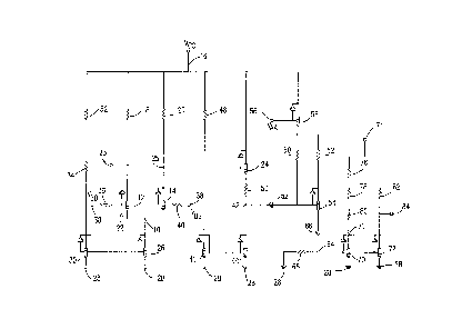
B_ief Description of the Drawing
The Figure is a schematic circuit diagram of a
preferred embodiment of the present invention.
Detailed Description of the Preferred Embodiment
The present inven~ion will be illustrated and
explained in the context of bipolar transistors.
However, it should be clear to one skilled in the art
that a variety of other switching devices may be
utilized in substitution for the bipolar transistors.
With respect to terminology, the current receiving
terminal of the transistor is meant to refer to that
terminal of the transistor which receives current,
i.e., the collector for the bipolar transistor, or the
drain for the field effect transistor. Likewise, the
current emitting terminal is meant to refer to that
terminal of the transistor which emits current, i.e.,
the emitter for the bipolar transistor or the source
for the field effect transistor.
Referring now to the Figure, the invention, in one
embodiment, comprises a first node 10, a first
transistor 12 with its current emitting terminal
connected to the first node, and a second transistor 14
with its cuxrent emitting terminal connected to the
;~ first node. The circuit further comprises a first
power supply line 16, a first resistor 18 connected
between the first power supply line 16 and the current
receiving terminal 23 of the first transistor 12. A
second resistor 20 is connected between the first power
supply line 16 and the current receiving terminal 25 of
the second transistor 14; A reference; for example, a
quartz crystal, is connected between the current
` receiving terminal 23 and the control input terminal 22
FI9-87-021 -3-
':
: , :
73~i
i
of the first transistor 12, with appropxiate load
capacitance provided from each of the terminals 23 and
25 to ground potential. A third transistor 24 is
disposed with its current receiving terminal connected
to the fixst power supply line 16 and with its control
input connected to the current receiving terminal 25 of
the second transistor 14. A fourth transistor 26 is
disposed with its current receiving terminal connected
to the first node 10 and with its current emitting
10 terminal connected to a second power supply line 28,
which may for example, be ground voltage. ~ first
constant voltage source is provided for biasing the
control line of the fourth transistor 26. In the
embodiment shown in the Figure, the first constant
15 voltage source comprises a diode 30 (a transistor with
; its collector and base shorted) and resistors 32 and 34
connected in series between the first power supply line
16 and the anode of the diode 30. The voltage drop
across diode 30 provides a constant voltage at the
20 control line of the fourth transistor 26.
It can be seen that the first and second
transistors 12 and 14 are connected as the switching
transistors for a current switch. The four~h
~ ~ transistor 25 operates as a current source for the
;~ 25 current switch. The first transistor 12 has its
control line connected through a resistor 35 to a first
reference voltage line 38. Likewise, the second
transistor 14 has its control line connected through a
resistor 40 to the first reference voltage line 38.
30 The transistors 12 and 14 and the load resistors 18 and
20 are specifically chosen in order to provide the
current switch circuit with a very low voltage gain of
on the order of 1.0 at terminal 23. In particular, the
voltage gains between the terminals 22 and 23 and
35 between the terminals 22 and 25 are maintained at a low
level. This level is just enough to assure oscillation,
so that the amplitude of the sine wave generated at the
terminal 22 is large enough to produce an appropriate
FI9-~7-021 -4-
77375
square wave at the terminal 25, while minimizing the
amplification of any noise injected at the terminal 22
or the terminal 23.
The circuit further.comprises a second node 42,
and a fifth transistor 44 with its current receiving
terminal connected to the second node 42 and with its
current emitting terminal connected to the second power
supply line 28. A second constant voltage source is
provided for biasing the control line of the fifth
transistor 44. In the embodiment shown in the Figure,
~ the second constant voltage source comprises a diode 46
(a transistor with its collector shorted to its base)
and a resistor 48. The diode 46 is disposed with its
cathode connected to the second power supply line 28,
and with its anode connected to one end of the resistor
48. The other end of the resistor 48 is connected to
the power supply line l6. The constant voltage drop
across diode 46 provides a constant voltage to bias the
~: control line for transistor 44.
~ 20 A third resistor 50 is connected between the
; current emitting terminal of the third transistor 24
and the second node 42. A first diode 52 is disposed
with its cathode connected to the second node 42. A
sixth transistor 54 is disposed with its control line
` 25 connected to the anode of the first diode 52. A second
reference voltage line 56 is provided with a voltage
which is different from the first and seconc. power
supply line voltages and the first reference voltage
line. A voltage source transistor 58 is disposed with
its control line connected to the second reference
~: voltage line and with its current receiving terminal
~: connected to the power supply line 16. A first
resistor network is disposed for providing current from
~: the voltage source transistor 58 to the current
receiving terminal of the sixth transistor 54 and to
the anode of the first diode 52. In the embodiment
shown in the ~'igure, this first resistor network
comprises a resistor 60 connected from the current
FI9-87-021 -5-
77~
emitting terminal of the transistor 58 to the anode of
the first diode 52, and a resistor 62 connected from
the current emitting terminal of transistor 58 to the
current receiving terminal of transistor 54.
The circuit further comprises a third node 64, and
a second diode 66 with its cathode connected to the
. third node 64 and with its anode connected to the
current emitting terminal of transistor 54. A fourth
resistor 68 is connected between the third node 64 and
the second voltage reference line 28. A seventh
transistor 70 is disposed with its control line
connected to the third node 64 and with its current
emitting terminal connected to the second voltage
reference line 28. An eighth transistor 72 is disposed
with its control line connected to the current
receiving terminal of the seventh ~ransistor 70, and
with its current emitting terminal connected to the
second power supply line 28. The output terminal 84
for the oscillator is connected to the current
receiving terminal for the eighth transistor 72. A
third reference voltage line 74 with a voltage which is
different from the first and second power supply lines
and the second reference voltage lines is provided for
powering the seventh and eighth transistors 70 and 72,
respectively. A second resistQr network is included
for providing power from the third reference voltage
line 74 to the current receiving terminals of the
seventh transistor 7~ and the eighth transistor 72. In
the embodiment shown in the Figure, this second
resistor network comprises the resistors 76, 78, and
80, connected in series, with one end of the series
connection connected to the third reference voltage
line 74, and with the other end of the series
connection connected to the current receiving terminal
of the seventh transistor 70. The second resistor
network further includes-a resistor 82 which i5
connected between the third reference voltage line 74,
and the current receiving terminal of the eighth
FI9-87-021 -6-
~.~773'7S
transistor 72.
In a preferred em~odiment of the presenk
invention, the first and the third reference voltage
lines are at the same voltage level. Additionally, the
diodes 52 and 66 may be implemented conveniently by
means of Schottky barrier diodes. Additionally, it is
desirable for many applications to connect a diode such
as a Schottky barrier diode across the base and
collector terminals of all of the transistors in order
to prevent transistor saturation.
It can be seen that the transistors 2~, 44, the
resistors 50 and 48~ and the diode 46 operate as a
level shifting and threshold adjusting circuit for the
square wave signal obtained from the terminal 25. In
particular, the waveform at the second node 42 is a
nearly-square trapezoidal function, whose midpoint can
be adjusted to coincide with a desired threshold
voltage by adjusting the value of the third resistor
50. The voltage drop across the third resistor 50
controls the voltage at the second node 42. In
essence, the node 42 voltage tracks the voltage at the
current-emitting terminal of the third tra~sistor 24,
with a prescribed voltage drop therebetween set by the
drop across the resistor 50. This resistor adjustment
can be used to compensate for duty cycle skews of
subsequent circuits attached to the oscillator (such as
an output driver) so that the overall duty cycle
remains approximately 50~.
It should be noted that the circuitry to the right
o~ the second node 42 is very similar to a diode
coupled receiver ~ith a direct-coupled inverter at its
-~ ~ output. This circuit functions to convert the ~oltage
at the second node 42 to the levels required by the
internal circuits of the logic gate array. It should
~` 35 be noted that the noise immunity for the overall
circuit is enhanced by this receiver-type output
because only noise that occurs during the rapid
transition through the threshold region can be
FI9-87-021 -7-
~.Z7~ 37S
propagated to the output of the circuit. This enhanced
noise rejection may be understood as ~ollows. If the
output terminal 84 is either at a high or a low
voltage, then any injected noise present at the
terminal 25 will not be able to switch that output
voltage level. It is only at the point where the
voltage level of the second node 42 is just high enough
to reverse bias the diode 52 and to turn on the sixth
transistor 54, that any noise present at the terminal
25 could have an effect in switching the transistor 54
on or off~ However, note again that amplitude of any
noise present at the terminal 2'; will be low because o~
the low gain of the current swit:ch circuit.
The diode-coup]ed receiver operates as follows.
When the second node 42 is at a low voltage, then the
diode 52 is biased into conduction and current flows
from the constant voltage source transistor 5$ through
the resistor 60, through the diode 52, and through the
fifth transistor 44 to the reference potential 28. No
current flowing through the resistor 60 flows toward
the control input of the transistor 54. The low
voltage at the cathode o~ the diode 52 is coupled to
the control line of the transistor 54, maintaining that
transistor in non-conduction. With the sixth
transistor 54 being in a non-conductive state, voltage
at the third node 64 remains low and the seventh
transistor 70, which has its control line connected to
the third node 64, is biased into non-conduction. The
current receiving terminal 71 of the seventh transistor
70 is thus at a high potential, so that the eighth
- transistor 72, with its control line connected to that
terminal, is biased into conduction. The transistor 72
thus draws current through the resistor ~2 resulting in
a voltage drop or low voltage at the output terminal
~4.
When the second node 42 rises to a high voltage,
the diode 52 is reverse biased. Accordingly, the
current drawn through the resistor 60 is applied to the
FI9-87-02l -8-
~.~7'73~;
control input of the sixth transistor 5~ and the
voltage at the control input rises so that the
transistor 54 begins to conduct. Current flowing
through the transistor 54 flows through the resistor 68
and provides a voltage drop thereacross, thereby
increasing the ~oltage at the third node 64. This
voltage increase in combination with the current flow
into the control line of the seventh transistor 70
brings that transistor into conduction. Transistor 70
thus draws current through the resistor 76, 78, and 80,
with a resulting voltage drop at the node 71. This
voltage drop at the node 71 is sufficient to bias the
eighth transistor 72 into non-conduction. With no
current flowing through the resistor 8~, the voltage at
the output terminal 84 rises to a high level.
It should be noted that the use of a constant
voltage source 58 connected to the reference line
voltage 56 allows the resistors 60 and 62 to connect to
a lower voltage, than the power supply line 16. If the
resistors 60 and 62 were connected directly to the
power supply line 16, then they would have to be larger
to provide the same current to the sixth transistor 54.
However, these larger resistors in combination with the
capacitances at the control line and the current
receiving terminals for the transistor 54 would provi~e
larger RC time constants, resulting in slower switching
operation for the circuit.
The present oscillator circuit provides a square
; wave with close to a fifty percent duty cycle while
maintaining high noise immunity. The circuit features
a double noise immunity by connecting an external
reference across a low gain current switch, and by
utilizing a diode-coupled receiver circuit which is
affected by noise only during the rapid transitions
through the threshold region of the square wave. The
circuit further features-a threshold circuit for
adjusting the voltage of the square wave signal and
applying the adjusted signal voltage to the input of
FI9-87-021 -9-
.,. . ~ . , ~ .. . . .
3~i
the diode~coupled receiver. Finally, this circuit
eliminates the need for the common-emitter-connected
first stage amplifier with its attendant noise
amplification problem.
While the present invention has been particularly
shown and described with reference to preferred
embodiments therefor, it will be understood by those
skilled in the art that the foregoing and other changes
in form and detail may be made therein without
departing from the spirit and the scope of the present
invention, as defined in the appended claims.
'
FI9-87-021 -10-