Note : Les descriptions sont présentées dans la langue officielle dans laquelle elles ont été soumises.
PHF . 86-!; 68C 1 1 . 7 .B7
Scintillation c~mera.
The invention relates to a scintillation camera,
comprising a scintillation crystal which may comprise a
collimator and which serves to convert each photon received
into a scintillation, a light guide for coupling said crystal
to the entrance window of an array of p photodetectors ~hich
serve to convert each scintillation into a current,
p acquisition channels which receive the output ~ignals of
said photodetectors and which supply p characteristic
electric signals which relate notably to the intensity
of the scintillations and to the distance between the
respective scintillation and each of the photodetectors,
and a processor which serves to supply the coordinates x; and
yj of a scintillation j and its associated energy Ej.
For the determination of the image of the radio-
active distribution inside an organ, medical diagnostics
utilizes inter alia the ccintigraphy principle. This method
is based on the introduction of a radioactive element into
the organism of a patient which attaches it.self more or less
to given organs, depending on whether these organs are
healthy or not. The measurement of the intensity of the
gamma radiation emitted provides an indication of the
distribution of the radioactive element in the organism and
hence forms a diagnostic aid. A measurement of this kind is
performed by means of a scintillation camera.
In conventional scintillation camerasl for example,
Anger type cameras (the physician Anger was the first one
to propose a scintillation camera whose principles are des-
cribed in United States Patent Specification No. 3,011,0~7),
the gamma rays which are representative of the radioactive
distribution in the environment examined penetrate a
scintillation crystal after having passed through a
collimator. The scintillations thus produced in the crystal
. ~
~ 7 ~ ~
P~ 86-568C 2 1.7.e7
are subsequently detected by a series of photomultiplier tuhes
(for example, 37) after having passed through a li~ht guide
which provides optical coupling between the crystal and the
tubes. These tuhes are distributed in front of the optical
5 block lcrystal + light guide) so as to cover substantially the
entire surface thereof and to convert the light energy of each
scintillation occurringinto a measurable electric signal.
Thus, with each photomultiplier tube there is asso-
ciated an analog acquisition channel which successively
10provides amplification, integration and shaping of the signals
supplied by the tube. The output signals Sij of the set of
acquisition channels are applied to a processor which supplies,
by estimation, the coordinates x; and yj of a scintillation j
and its energy Ej (the index i designates the relevant
15acquisition channel). The processor may comprise several types
of calculation devices, but essentially two thereof are used,
in practice, i.e. an arithmetical calculation device for
determining the bary centre.
In such an arithmetical calculation device, the
20quantities Xj, yj, Ej are given by the expressions:
xj = I (1)
Yj Z (2)
~ --1 G i S i j
1--
In these expressions:
1--1 i i j
Yj i~ 5)
j i~-l Ji Sij (6)
where the coefficients Gi, Ki, Hi, Ji are weighting factors
related to the position of the axis of each of the p photo-
multiplier tubes.
~4~7~
PHF.86 568C 3 1.7.87
In such a logarithmic calculation device, the
quantities Xj, yj, E~ are given by the expressions:
x+
Xj = a Log 1 (7)
Yj = a Log -~ (8)
Ej = 51 Gi Sij l9)
X~ = ~ Ki Sii
X j = 5 K i i j ( 1 1 )
+ i -p + ( 12 )
Yi = ~1 Hi ii (13)
25 The weighting factors are again related to the position
of the axis of each of the p photomultiplier tubes.
Regardless of the arithmetic used, contemporary
scintillation cameras generally comprise devices for
calculating weighted sums which utilize resistance networks
30 with associated summing amplifiers. In the cameras of this
type it is not possible to execute calculations relating to
a scintillation before the signals corresponding to the pre-
ceding scintillation have been set to zero, so that the
maximum calculation speed is limited. In order to increase
35 this speed, various solutions have already been proposed,
for example the reduction of the duration of the electric
signals or the integration time by means of analog circuits.
4~3
-~- 20104-8340
However, such a reductlon ~ould be clchiev~d only at the expense of
given intrinsic characteristics of the cameras, notably the spatial
and the spectral resolution.
In a previous Fren~h Patent Application FR~A 2 552 233
Published on March 22, 1985, Applicant has proposed a digital
radiation measuring device in which it is no longer necessary for
the electric signals to return to zero before each new measurement,
which means that a partial pile-up of the detected scintillations
(and hence of the electric signals or pulses corresponding thereto)
is accepted.
It is the ~bject of t~;e invention to propose a novel
scintillation camera which incorporates given elements of the above
device which, however, are arranged partly within the p acquisition
channels and partly within the processor and which has a simplified
electronic design which allows for the A/D conversion and the
subsequent digital integration of the signals to be performed by
means of less accurate and hence less expensive converters. This
design also enables the execution of unpiling calculations by means
of a limited number of processing circuits.
To achieve this, the scintillation camera in accordance
with the invention is characterized in that: (A~ said p acquisi-
tion channels sample said output signals of the photodetectors,
followed by the A/D conversion of the samples obtained and their
summing, and apply p digital signals to the iA put of the processor;
(B) the process itself comprises: (a) a bus for transferring said
digital signals; (b) a digital summing stage, comprising four
~5~ 1'2~77447 20104-8340
digital weighted sum forming devices which supply four digital
signals Xm, Ym~ Zm~ Em on the basis of the output signals of the
p acquisition channels; (c) a scintillation processing stage which
includes unpiling calculation circuits and two dividers and which
supplies the three coordinate and energy signals x, y, E, on the
basis of the signals Xm, Ym~ Zm~ Em; (C) a detection, sequencing
and storage stage which receives a signal which corresponds to the
sum of the p output signals of the photodetectors is provided in
order to supply on the one hand the various clock signals for
synchronizing the elements of the p acquisition channels and the
elements of the processor, and on the other hand the correction
coefficients for the scintillation processing stage.
For example, European Patent Application No. 0166169
Published on February 1, 1986 describes a scintillation camera
which realizes the A/D conversion only in the processor; this
notably leads to the use of high-precision and components which
are far more costly, i.e. with a ratio of at least 1 : 100.
The particularities and advantages of the invention will
become apparent from the following description, given by way of
example, with reference to the accompanying diagrammatic drawings;
therein: Figs. 1 and 2 show a scintillation camera in accordance
with the present state of the art and in accordance with the
invention, respectively; Fig. 3 shows an embodiment of the
conversion and integration device of each of the p acquisition
channels; Fig. 4 shows a first embodiment of the processor of a
scintillation camera in accordance with the invention; Figs. 5a to
... . .
.
. . .
-5a~ 7~ 20104-8340
5c show the individual signals corresponding to approximated
scintillations causlng a partial pile-up, the overall signal
resulting from this pile-up, and the shape of the signal represent-
ing the measured value resulting from the summing of the samples
during the time interval ~j~ j+l for the channel i (this value
having been measured at the instant t ~j+l)' respecti~ely; Fig. 6
shows an embodiment of one of the unpiling calculation cirCuits of
the scintillation processing stage; Fig. 7 shows an embodiment of
the detection, sequencing and storage stage; Fig. 8 shows an alter-
native embodiment of the unpiling calculation ~ircuit shown in Fig. 6;
Fig. 9 shows a second embodiment of the processor of a camera in
accordance with the invention, which includes
~ ~ ~ 7 4 L"'l 7
PHF . 86--5 6~3C ~ 1, 7 . 87
the alternative embodiment of the unpiling calculation
circuit shown in Fig.8;
Fig. 10 shows a third embodiment of the processor
of a scintillation camera in accordance with the invention
5 which includes a third embodiment of the scintillation
processing stage;
Figs.11 to 13 and 14 to 16 show, analogous to the
Figs. 4, 9, 10, the modifications tothe processor ~hen only
three calculation channels X, Y, Z or X, Y, E, respectively,
10 are used;
Fig. 1 7 shows an embodiment of a weighted sum
calculation device in accordance with the invention; and
Fig. 18 shows the shape of various signals present
at various points in the device shown in Fig.17.
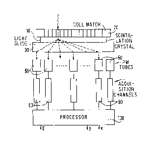
The conventional scintillation camera shown in Fig.1
comprises a scintillation crystal 10 which is provided with
a collimator 20 and which is intended for converting each
photon received into a scintillation. Via a light guide 30,
the crystal is coupled to the entrance window of an array of
20 p photodetectors which are in this case formed by photo-
multiplier tubes 50. The tubes 50 convert each scintillation
into a current which is then processed by p fully analog
acquisition channels 60. The acquisition channels 60 realize
notably the amplification, filtering, integration and shaping
25 of the output signals of the photomultiplier tubes 50 and
are followed by a processor 100 which supplies the coordinates
Xj, y~ and the energy Ej.
In the embodiment which will be described in detail
hereinafter with reference to Fig. 2 which shows the
30 modifications to the circuit diagram of Fig. 1 for a camera
in accordance with the invention, the p acquisition channels
60 are no longer fully analog like in conventional cameras~
but apply p digital signals Mi j (i = index varying from 1
to p) to the input of the processor 100. The p channels now
successively provide the amplification, filtering and
sa~pling of the output signals of the photomultiplier tubes
50 after the A/D conversion of the samples obtained and the
PHF.86 5~8C 7 1.7.87
summing of the digital samples. The value of the p digltal
signals is related to that of the output current of the tubes
50 and hence to a fraction of the intensity of the initial
scintillation, but clifferent in accordance withthe pile~up
5 rate of the scintillations (this fraction itself is related
to the realization of the optical block and notably to the
distance between the scintillation point and the axis of the
tubes)~ If there were no pile-up, the value of each of these
signals would be denoted as Sj j; the estimation of these
ln values in the presence of pile-up will be denoted in Si j.
For realizing the above functions each of the p
channels thus comprises a series connection of an
amplification and filtering circuit 61 which receives the
output. signal of the corresponding tube 50, a time realignment
15 circuit 62 which is followed by a conversion ana integration
device 63 which proviaes the successive sampling of the
output signals of the corresponding circuit 62, the A/D
conversion of the signals thus obtai.ned, and the summing
thereof. There is also provided an analog summing amplifier
20 64 whose p inputs receive the p output signal.s of the
amplification and filtering circuits 61 and whose output
signal is applied to a pulse-start detector which is situated
in the detection, sequencing and storage stage 400 to be
described hereinafter. The output signal of each of the p
2s conversion and integration devices is applied to the
processor 100, possibly via p FIFO memories which enable
later operation at much lower frequencies thus by controlling
the output of scintillations~ This array of FIFO memories
actually enables a reduction of the speed of later
30 calculations and the slower rhythm thus ohtained may be
practically equal to the means arrival rhythm of the
scintillations (for example, 2 microseconds for a mean
rhythm of 500,000 scintillations per second) and no longer
equal to the arbitrary arrival rhythm of the scintillations
(approximately 0.2 microseconds in the former case). Each of
the the conversi.on and integration devices 63 used herein is
equivalent to that disclosed in French Patent Applicat:ion
7~
PilF,86-568C 8 1.7,87
FR-A 2 552 233 an~ comprises, in the embodiment shown in Fig.3,
a sampling and D/A con~ersion circuit 310 w~ich is followed
by an adder 311. To the output of the adder 311 there are
connected a first register 312 for storing the output signal
5 of the adder, the output signal of the register being applied
to a second input of the aader, and a second re~ister 313 for
storing the output signal of the adder, the output signal
of the second register being that of the conversion and
integration device which thus realizes a cumvlative
10 addition and the corresponding storage as the samples arrive.
These operations are performed under the control of the
detection, sequencing and storage stage 400 to be described
hereinafter.
The processor 100 receives the p output signals of
15 the acquisition channels and comprises various calculation
devices for distinctly determining the coordinates Xj, yj
and the energy Ej of each scintillation j, either by means
of the relations (1~ to (6) in the case of an arithmetical
calculation device or by means of the relations (7) to (13)
20 in the case of a logarithmic calculation device.
Mcre precisely, the processor 100 as shown in Fig.4
is constructed as follows in the case of an arithmetical
calculation device. It comprises first of all a bus 150
for transferring the digital signals Mi j present at the
25 output of the p acquisition channels. If for one of these
channels, for example the channel i, the individual analog
signals associated with several scintillations wich are
grouped in time (Fig. Sa) and the resultant pile-up signal
of these individual signals are represented (Fig. 5b),
30 it appears th~t the scintillation j is disturbed upstream
by several scintillations j-1, j-2, etc. If ~j and Yk j
are coefficients for correction by extrapolation and inter-
polation, respectively, which can be determined from the
known mean shape, as a function of time, of the pulses
35 corresponding to a detected scintillation and from the
measurement of the period ~j j+1 between to j and to j+1~ if
k is successively equal to j~ 2,...... j-q, and if the
t7~
PHF.86-568C g 1.7.87
signals Sik represent for these respective values of k
the values corrected for pile-up effects which wou].d be
supplied by the digital acquisition channel in reaction
to the scintillations j-1, j-2, ..., j-Q, the digital signals
5 obtained at the output o~ the acquisition channels will be
shaped as:
i,j ;~ j ~=~ 1 k,j i,k (14)
where Mi j represents the value measured at the i.nstant
to i+1~ resulting from the summing of the samples during
the time interval ejj+1 for the channel i. The shape of the
signal Mi j -'5 shown in Fig. 5c.
The processor finally comprises, connected to the
output oE the transfer bus 150, a digital summing stage 200
which itself is composed for four digital weighted sum forming
devices 201 and 204 as shown in Fig. 4. The four devices 201
to 204 form the following weighted sums:
20 Xm j = i Ki ii (15)
Ym~j i i ij (16)
25 Zm j = ~i Ji ii (17)
Em j = i Gi ij (18)
respectively, where the coefficients Ki, Hi~ Ji~ Gi are the
digital expressions of the weighting factors defined in
30accordance with the expressions (3) to (6)(for an arithmetical.
calculation device). Each of the digital weighted sum forming
devices is, for example of the type multiplier-accumulator
TDC 1009 (marketed by TRW, La Jolla, CA 92038, USA), one of the
inputs of which receives the corresponding output signal of
35the bus 150, its other input receiving the weighting
coefficients (in digital form), which are stored in an
auxiliary memory. When this type of multiplier accumulator
.1 ~77L~
PHF`.8~-568C 10 1.7.87
is effectively u~ed, said auxiliary memory must be
synchronized with the operation of the complete processor
and may be incorporated, for example in the ~etectionf
sequencing and storage stage 400 to be descrihed hereinafter.
The output signals Xml Ym~ Zm~ Em
summing stage 200 are thus applied to a scintillation
processing stage 500. As appears from Fig. 4, the stage 500
comprises four unpiling calculation circuits 501 to 504,
two dividers 505 and 506, and one time realignment circuit
lO 507. Because the four circuits 501 to 504 are identical,
only one thereof will be described, for example the circuit
501. This circuit is shown in Fig. 6 and comprises a sub-
tractor 510 whose first, positive input receives the output
signal of the corresponding digital weighted sum forming
15 device 201 (the circuits 501 to 504 correspond to the
devices 201 to 204, respectively). The subtractor 510 is
followed by a first multiplier 511 and a storage register 512,
the output of which is that of the circuit 501. The subtractor
510 is also followed, connected parallel to the elements 511
20 and 512, by a second multiplier 513 and a second storage
register 514. These multipliers may be replaced by a single
multiplier circuit in association with a time multiplexer/
demultiplexer. The negative input of the subtractor 510 is
connected to the outp~t of the storage register 514. The
25 The second input of the multiplier 511 is connected to the
output of a memory 470 which stores the coefficients ~j
and that of the multiplier 513 is connected to the output of
a memory 480 which stores the coefficient Yj k. For the
scintillation j the outputs X, Y, Z, E of the four unpiling
30 calculation circuits 501 to 504 are given by the expressions:
X~ tXm j ~ k~j 1 k,j (19)
Yj = ~j ~Ym j ~ k~j 1 k,j k~ (20)
Zj ~ m,j kj 1 ~ k,j ~k~ (21)
E = ~j ~Em j ~ j 1 Y k,j k~ (22)
77~7
PHF.86-568C 11 1.7.87
The elements o~ each circuit 501 to 504, for example
the e]ements 510 to 5~4 of the circuit 501, form an upiling
c~lculation circuit which is equivalent to that described
in French Patent Application FR-A 2 552 233 and denoted by
5 the reference numerals 120 to 160.The other three circuits
502 to 5~4 co~prise the same elements as the circuit 501.
The output signal X of the unpiling calculation
circuit 501 is applied to the first input of the divider 505
and the output signal Y of the circuit 502 is applied to the
first input of the divider 506. The second input of each of
these dividers is formed by the output Z of the unpiling
calculation circuit 503. The three output signals of the
processing stage, also being those of ~he processor, are
formed by the output signal Xj = Xj/Zj of the divider 505,
15 the output signals Xj = Yj/Zj of the divider 506, and the
output signal Ej of the time realignment circuit 507
connected to the output of the unpiling calculation circuit
504. In the processor the detection, sequencing and storage
stage 400 is also associated with these elements. The stage
20 400 is shown in Fig.7 and comprises first of all a pulse
start detector 410 which receives the output signal of the
analog summing amplifier 64 (see Figs. 2 and 4). The detector
410 is followed by a clock circuit 420 and a clock signal
counter 430. The number thus counted is applied to a test
25 circuit 440 whose output signal is applied to the sequencing
circuit 450. The latter circuit synchronizes the operations
performed in the acquisition channels, the stage 200 and the
stage 500, and validates the contents of a register 460 for
storing the output signal of the counter 430, the register
30 460 being connected parallel to the test circuit 440. To the
output of the register 460 there are connected the two
memories 470 and 480 mentioned above with reference to Fig.6
and storing the coefficients ~j and ~j k~ respectively.
The above elements 410 to 480 form a detection sequencing and
35 storage stage which is similar to that disclosed in the
Application FR-A 2 552 233.
4~7
P~IF.86-568C 12 1.7.87
In a second embodiment, the calculation of the
scintillation coordinates can be realized, without introducing
extrapolation, in accordance with the following expressions:
6 x'j = xm,j ~-1 k,j k (2
Y j Ym,j k~ 1 k,j k !24)
Z ~ j = Xm ~ A (25)
where always Xj = X'j/Z'j and yj = Y'j/Z'j . The correction
eoeffieient Ck j is a function of ej j+1 and of ek j- In this
embodiment, the scintillation processi.ng stage is denoted
by the reference numeral 600 and the three unpiling
calculation circuits which receive the signals Xm, Ym~ Zm
are modified by the omission of the multiplier 511. These
circuits actually have the construction shown in Fig.8 for
an arbitrary one of these circuits, for example the first
20one of the circuits 601 to 6030 The circuit 601 comprises
a subtractor 610 which receives on its first input the output
signal of the corresponding digital weighted sum forming
device 201. The subtractor 610 is followed on the one hand
direetly by a storage register 612 whose output is that of
25the unpiling calculation cireuit as before, and on the other
hand, in parallel, by a multiplier 613, followed hy a storage
register 614. The output signal of the register 614 is applied
to the second input of the subtractor 610, the other input
of the multiplier 613 bei.ng eonnected to the output of the
30 memory 480 included in tne stage 400 for the storage of the
coefficient y . The other two circuits 602 and 603 comprise
similar elements. The unpiling calculation circuit 504 re~
maining the same, the construction of the processor 100 is
now as shown in Fig.9O As before, the energy E is avai.lable
35 on the output of the time realignment circuit 507.
In a third embodiment as shown in Fig.10, the
processor 100 comprises a third type of scintillation
.J744~
PHF . ~6--5 ~3C 13 1 . 7.87
pr~cessi~g stage which is denotea by the reference numeral
700.In this emhodiment the unpi~ing operati~n is no longer
performed on the ou~.put slgnals xm, Yml m
summing stage 200 bu~ on the coordinates xm and Ym, said to
5 have been measured because for each scintillation j they are
derived directly from the non-correctedquantities Xm, Ym Zm
in accordance wi-th the relations xm j=Xm j/~m j and
Ym j = Ym j/Zm j These signals xm and Ym are o~tained on the
output of the two dividerc 705 and 706, the divider 705
0receiving the output signals of the digital summing devices
201 and 203 t whilst the divider 706 receives those of the
devices 202 and 203. The coordinates Xj, yj corresponding to
the scintillation j are thus obtained on the outputs of the
unpiling calculation circuits 701 and 702 on the basis of on
15 the one hand said measured data and on the other hand on the
basis of the already known coordinates xk~ Yk of the preceding
scintillations which disturb the scintillation j, in accordance
with the following expressions:
xj = xm j ~ j q ~ k,j (xk m,j) (26
Yj = Y j ~ ~ q r k,j (Yk Ymlj (27)
The coefficients rk j~ being a function of the measured time
intervals j j+1' k j and the ratios Ek/Ej, are calculated
in an additional calculation circuit 707 which receives on
the one hand the output signal E ofthe unpiling calculation
30 circuit 504, whichis always included in the processing stage~
and on the other hand the coefficients~ and ysupplied by the
detection, sequencing and storage stage 400. In the precent
embodiment the circuit 707 calculates on the one hand, based
on the values of E successively received, the successive
35 ratios Ek/Ej and, on the other hand, the products ~j Yk j on
the basis of which the coefficients rk j are evaluated in
accordance with the relation r k j = ~j Yk j Ek/Ej .
4~3
P~3F.86 5h~C 14 1.7.87
The unpi ing calculation circuits 701 and 702 have a
configuration which is similar to that of the circuits 601
and 602. As before, the ener~y E is available on the output
of the time realignment circui-t 507.
It is to be understood that the i~vention is not
restricted to the embodiments described and shown, for which
many alternatives are feasib~e without departing from the
scope of the invention. For example, there may be provided
an amplitude rejection circuit for reducing the number of
l0 scintillations to be processed, so that ca~culations are
performed only on selec~ed scintillations (by means of a
threshold, an energy window, etc.). On the otherhand, there
may be provided a time multiplex circuit so that only one
divider need be used instead of two in each of the embodi.ments
15 shown in the Figs. 4, 9 and 10. A time multiplex circuit
may also be provided in order to reduce the number of unpiling
calculation ci.rcuits, so that only one ~npiling calculation
circuit need be used instead of the four circuits 501 to 504
in the embodiment shown in Fig. 4, the four circuits 601 to 603
20 and 504 in the embodiment shown in Fig.9, or the three
circuits 701, 702 and 504 in the embodiment shown in Fig.10.
The series of alternatives proposed inthis section is al.so
applicable to the other embodiments according to the Figs.11
to 16.
Taking into account the means for the correction of
linearity errors and energy errors utilized by state of the
art gamma cameras on the basis of the signals x, y and E
on the output of the processor, Z or E can be used arbitrarily
for the calculation of the coordinates. In that case only
30 one of these quantities can be calculated and, depending on
the choice made; the other quantity can be deduced from
calculations in which specific corrections for this choice
are made and which are executed by said means. The digital
summing stage 200 thus oomprises only three digital weighted
35 sum forming devices which supply the signals X~, Ym, Z or
Xm, Ym, Em, respectively. Moreover the scintillation
processing stage 500 comprises only three unpiling calculation
PHF.86~5~8C 15 1./.~7
circuits. Similar to the Figs. 4, 9 and 10, the Figs. 11
to 13 show the modifications in the processor when only
three channels X, Y, Z are uced~ whilst the Figs. 14 to 16
show, again similar to the Figs. 4, 9 and 10, the
5 modifications of the procescor when only three channels
X, Y, E are used.
On the other hand, it is also to be noted that, in
order to enab]e operation at lower frequencies by controlling
the scintillation rate, reaa/write FIFO memories which are
10 controlled by the detection, sequencing and storage stage 400
can be arranged upstream from the digital summing stage.
Finally, it is to be noted that the bus 150 is either
incorporated in the processor in which it forms the input
or access element, or is connected thereto without being
15 included therein.
The weighted sum forming device in accordance with
the invention which is shown in Fig.17 comprises a digital
multiplier 220 which se~uentially receives, via a first shaping
circuit 209, the sicrnals for which the weighted sum is to be
20 formed, an adder/accumulator 23C, and a second shaping
circuit 240. The first shaping circuit 209 essentially
serves to restore the shape of the signals which, upon
arrival, may have been disturbed hy the circuits previously
traversed, whilst the second shaping circuit 240 realizes,
25 in addition to shaping, a current gain and/or impedance
matching.
A digital memory 250 supplies the digital
multiplier 220 with weighting coefficients to be applied
to said signals. Commercially availahle integrated circuit
30 digital multipliers (some of which also incorporate the
adder/accumulator) can operate on signed as well as non-
signed data. Thus, either positive or negative weighting
coefficients can be stored in the digital memory 250.
A processing circuit 210 is connected in series
35 between the first shaping circuit 209 and the digital
multiplier 220. The circuit 210 is controlled by a clock
signal which will be described hereinafter. In the present
~l ~77~
PHF.86-5fi8C 16 1.7.87
embodiment a dlgital register 211 which contains a (possibly
variable) threshold value (including the range to the value
O) is connected to the processing circuit 210. The processing
circuit 210 may be formed simply by a circuit for eliminating
5 signals which are below said threshold, or by a circuit
having a more complex construction.
In a first embodiment, the digital memory ~50 is a
ROM, The coefficients ~tored therein are thus permanently
~ixed during manufacture. In a more elaborate embodiment,
10 the mem~ry 250 may be a RAM. The weighting coefficients can
then be mo~ified by means of an additional wire or micro-
programmed circuit (microprocessor, microcomputer, ...).
The operation of the weighted sum calculation device
in accordance with the invention will be described hereinafter
lS with reference to Fig.18 which shows the shape of the signals
present at various points in the device.
The digital signals present on the input of the
shaping circuit 209 are denoted by the references
S1~ S2, ..., Si, ..., Sp, -- etc. and are shown in Fig.18a.
20 After shaping, these signals are received by the processing
circuit 210 in the rhythm of the clock signal which is shown
in Fig.18b and with which the arrival of the digital signals
S1, S2, ..~, Sp, ..., is synchronized. This clock signal
is received on the connection 212. In the described
25 embodiment,the circuit 211 defines the threshold value and
the output signals of the circuit 209 are applied, or not,
to the digital multiplier 220, depending on whether there are
larger than/equal to or smaller than said threshold value,
respectively.
The signals present on the output of the processing
circuit 210 are thus multiplied by respective weighting
coefficients in the rhythm of a ~ignal supplied on the
connection 222. This signal is shown in Fig. 18c and is
identical to that shown in Fig. 18b, but has been delayed
35 with respect thereto by a period of time necessary for the
transfer of the signals. The weighting coefficients are
supplied by the memory 250 which is addressed in the rhythm
7~
P~-IF.86-568C 17 1.7.87
of the signal which is shown in Fig.18d, which is present
on the connection 252 and which is in phase with the signal
shown in Fig.18a.
The adder/accumulator 230 thus performs a progressive
5 summing operation on the weighted digital signals appliea to
its input, i.e. in the rhythm of the signal sho~n in Fig.18e
which is identical to that sh~wn in Fig. 18b but which has
also been de~ayed (in a manner other than in the preceding
case) with respect thereto in order to compensate for the
10 signal propagation time. The signal shown in Fig. 18e is
received on the connection 232, a connection 234 being
provided for the supply of a signal for resetting the adder/
accumulator to zero (see Fig.18f). Finally, Fig.18g shows
a validation signal which is applied to the connection 242
15 of the shaping circuit 240 and which makes the desired
weighted sum signal available on the output of the circuit
240. This sum signal is shown in Fig.18h (the state preceding
its arrival is referred to as a high impedance state).
In the described embodiments or in the alternatives
20 which can be realized within the scope of the invention,
the weighted sum calculation device in accordance with the
invention can find an important application in the field of
scintillation cameras.