Note : Les descriptions sont présentées dans la langue officielle dans laquelle elles ont été soumises.
~7~ 9
1 5~,930
MUL ~ URPOSE DIGITAL INTEGRATED_CIRCU T FOB
_O~ UNICATIOU AND CONTROL NETWORK
CROSS REFERENCE TO RELATED APPLICATION
The invention disclosed herein relates to two-
way communication and control systems. The following
commonly assigned Canadian patent application relates to
such communication and control systems; Serial number
484,817 filed June 21, 1985, by Leonard C. Vercellotti,
William R. Verbanets Jr. and Theodore H. York entitled
"Digital Message Format for Two-Way Communication and
Cont.rol Network".
This application is a divisional of Canadian
patent application s0rial number 484,816 entitled
"MULTIPURPOS~ DIGITAL INTEGRATED CIRCUIT FOR
COMMUNICATION AND CONTROL NETWORK." Other divisionals of
that application, and bearing the same title, are
Canadian paten~ applications:
serial numbers 594,777; 594,778; 594,948; 594,947; and
~9~,949
BACKGROUND OF THE INVENTION
;
A. Field of the Invention
The present invention relates generally to
information communication networks and, more
particularly, to communication networks by means of which
25a large number of remotely positioned controllable
davices, such as circuit breakers, motor overload relays,
lighting systems, and the like, may be controlled from a
central or master controller over a common network line
which may comprise either the existing AC power lines, or
~;~i7E3~
2 51,930
a dedicated twisted pair line, or in some instances a
fiber optic cable.
The invention particularly relates to a low
cost, multipwrpose digital integrated circuit (IC) which
can be ussd as the basic building block in astablishing
a network communication system over a desired
communication link. The digital IC can function as an
addressable microcomputer interface between the network
line and a remotely located microcomputer which may, for
example, comprise any microprocessor based controlled
product. In such mode, ths digital IC's function is to
take data from the network and pass it on to the remotely
located microcomputer upon command from the central
controller and to transmit data from the microcomputer to
the central controller. The digital IC may also function
as a nonaddressable microcomputer interface between the
central or rnaster controller and the network line. In
such case the digital IC's function is to continuously
take data from the central controller and place it on the
network and take data from the network and pass it back
to the central controller. The digital IC may also
function as an addressable load controller associated
with an individual remote controlled device and
responding to shed or restore load commands from the
central controller over the network line. When so usad
the digital IC may also be commanded to transmit a reply
message back to the central controller giving information
as to the status of the controlled device, thus enabling
the central controller to monitor a large number of
remotely located controllable devices.
B. DescriPtion of_the Prior Art
Variouscommunication and control systems have
been heretofore proposed for controlling a group of
remotely located devic~s from a central controller over
;
:
31L~78~
3 51,930
a common network line. Control systems For controlling
distributed electrical loads are shown, for example, in
Miller et al's U.S. patents Nos. 4,167,786, issued
September 1979, 4,367,414, issued January 1983, and
~,396,~44, issued August 1983. In such systems a large
number of relatively complex and expensive transceiver-
decoder stations, each of which includes a
microprocessor, are interconnected with a central
controller over A common party line consisting of a
dedicated twisted pair for bidirectional communication
between the central controller and all transceivers.
Each of the transceiver-decoder stations is also of
relatively large physical size due to the fact that a
substantial amount of hardware is required, in addition
1~ to the micro-processor, to receive and transmit signals.
Also, both the hardware and microprocessor consume
substantial amounts of power. In fact, in Miller et al's
U.S. patent No 4,167,786 it is necessary to provide a
powersaver mode in which the major portion of the
circuitry at each remote station is de-energized to
reduce power consumption during intervals when load
changes are not being actuated.
Each of the transceiver-decoder stations
control~ a number of loads which must be individually
conn~cted to a particular transceiver by hardwiring,
these interconnections being quite ler,gthy in many
instances. In such a system, all transceivers can
initiate messages at any arbitrary time in response to
control input from the associated switches. Accordingly,
it is not uncommon for two or more transceivers to
simultaneously sense a free common party line and begin
; simultaneous transmission. This requires a special bus
arbitration scheme to cause all but one of the
interfering transceivers to drop out of operation while
permitting one selected transceiver to continue its data
transmission. Also, in such a system transmission from
~, .
~8(~
4 51,930
the transceiver to the central controller is very limi-ted
and consists merely o~ an indication of a manually
operable or condition responsive switch or analog sensors
such as a thermistor or other analog sensing device. In
the load distribution control system shown in the above
referenced prior art patents, the arbitration technique
is dependent on the impedance levels of the active and
inactive states of the data line. If the data line
becomes stuck in a low impedance state, due to the
failure o~ one o~ the connected transceiver decoders,
further c~mmunication over the network line is prevented
until the malfunctioning transceiver is physically
disconnacted from the data line.
In the communication and control system
described in the above identified Miller et al patents a
message transmitted ovor the network includes a preamble
portion o~ a minimum of four bits. These preamble bits
comprise 50% square waves which are utilized by the
transceiver decoders to permit a phase lock loop circuit
in each transceiver to lock onto the received preamble
bits. The use of a minimum of four bits to provide phase
loop lockon reducas the overall throughput of such a
system. Also, in order to capture the preamble bits, it
is necessary to provide the phase lock loop circuit
~ 25 initially with a relatively wide bandwidth of about 5KH2- and then narrow down the bandwidth after the phase lockloop circuit has locked onto the preamble bits. Such an
arrangement requires additional circuitry to accomplish
the necessary change in bandwidth. Also, the relatively
wide bandwidth necessary to capture the preamble bits
also lets in more noise so that the security and
reliability of the system is reduced in noisy
environments.
SUMMARY OF THE INVENTION
According to one aspect of the present
invention, there is provided, in a communication and
"'
s~
~ 51,930
control system, a digital integrated circuit (IC~ device
having a transmit output tsrminal coupled to a common
network line of said system, means in said device for
supplying a message start signal to said transmit
terminal having a predetermined logic value and a
duration of two bit intervals at a predetermin d baud
rate, and means in said device for supplying message data
bits stored in said device to said transmit terminal
immediately following said start signal. One of said
data bi~s comprises a control bit having a first logic
value which designates a plurality o~ message bits as
instruction bits to enable an interface to be set up
be~ween said common network line and a microcomputer.
The other logic value of said control bit designates a
plurality of message bits as data bits for said
microcomputer after said interface has been enabled.
In preferred embodiments o~ the communication
network a small low cost digital integrated circuit is
employed which can be readily adapted by merely grounding
different input terminals o~ the IC to perform all of the
different functions necessary to the component parts of
the completer communications network. Thus, in one pin
con~iguration of the digital IC it can function as an
addressable load conkroller, responding to shed or
restore load commands from the central controller and
replying back to the central controller with s-tatus
information regarding the state of the controlled load.
This mode of functioning of the digital IC is refsrrad to
as a stand alone slave mode of operation. In the stand
alone slave mode the digital IC is arranged to be
directly associated with each control device i.e. circuit
breaker, motor controller, lighting control, etc. and
may, if desired, communicate with the master controller
over the same wires which are used to supply power to
the controlled device. This substantially reduces the
amount of wiring required to connect a number of
.. ..
~78~
6 51,930
controlled devices to the common communication network.
The central controller may also issue block shed and
block restore commands ko a group of stand alone slaves
to which command they will all simultaneously respond.
Also, the central controller may issue a "scram" command
to shed load which causes all stand alone slaves (which
may number as high as 4,095) to simultaneously shed their
respective loads.
In another pin configuration of the digital IC
it can function as an addressable microcomputer
interface. In this so called expanded slave mode of
operation the digital IC provides an interface between
the communication network line and a remote microcomputer
which may, for example, wish to transmit data over the
communications network to the central controller. In
the expanded slave mode of the digikal IC the micro-
computer interface is disabled until the cantral
controller enables it by sending an enable interface
command addressed to the expanded slave. After the
microcomputgr interface i5 enabled the central controller
and the remote microcomputer can communicate back and
forth through the expanded slave digital IC.
The digital IC may also be pin configured to
function as a nonaddressable microcomputer interface7
such functioning being referred to as the exp~nded master
mode of functioning of the digital IC. In the expanded
- master mode the interface with an associated
microcomputer is always enabled and any network
transmissions that the digital IC receives may be read by
the interfaced microcomputer. Also, the interfacad
microcomputer may transmit data onto the network at any
time through the expanded master type of digital IC.
Accordingly, when the digital IC is operated in this mode
the interfaced microcomputer may comprise the central
controller of the communications network.
~:,
.
~7~
7 51,930
The digital IC which may be adapted to perform
all of the above described functions, may also be
arranged so that it can be used with different types of
data lines. Thus, in one embodiment the digikal IC is
adapted to transmit messages to and receive messages-from
a network line consisting of the conventional AC power
line of a factory, office building or home. Because of
the significant phase d i stu rbances associated with such
power lines, data is transmitted over the network by
means of on-off keying of a high frequancy carrier.
Preferably this high frequency carrier has a frequency
of 115.2 KHz and the digital IC is arranged to transmit
data at the rate of 300 bits per second (300 baud) over
conventional power lines. The choi ce of a 115.2 kHz
carrier is based on empirical results of spectru~
analyses of typical power lines and the 300 baud bit rate
is based upon desired system performance and accPptable
error rates.
Ths digital IC may comprise a crystal
~0 controlled oscillator operating at a frequency ~any times
higher than the carrier fre~uency. The carrier signal is
derived from this crystal oscillator. The crystal
oscillator is also used aæ a source of timing signals
within each digital IC to establish predeter~ined baud
rates for thQ transmission of data over the network.
Accordingly, the frequency of the carrier signal employed
to transmit messages over the network can be readily
; changed to avoid an undesired interfering frequency by
s-imply changing the crystals in the crystal oscillator
associated with each di~ital IC. Such a change in
carrier ~requency will also change the baud rates at
which the communication systsm opsrates, as described in
more detail hereinafter.
The frequency of the crystal oscillator in
each digital IC preferably is highly stabilized so that
the carrier frequencies developed by the digital IC's at
,
-' ; ` ~ . ':`,' ! : ~
8 51,930
the central controller and remote stations are very close
to the same frequency although a received carrier signal
may drift in phase relative to the timing signals
produced in the digital I~ which is receiving a message.
As a result, it is nok necessary to transmit a number of
preamble bits and provide a phase lock loop circuit which
locks onto the received message dur1ng the prea~ble bits,
as in the above described Miller et al patents. In
embodiments of the presant invention the indiYidual
digital IC's may operate asynchronously but at
substantially the same frequency so that any drift in
phase does not interfere with detection of the received
carrier signal, even at relatively low baud rates and
noisy environments.
In order to provide further noise immunity
when using noisy power lines as the common network data
line, the digita1 IC may be arranged to compute a 5 bit
BCH error code and transmit it with each message
transmitted to the network. Also, each message rec~ived
from the network by the digital IC includes a five bit
BCH error code section and the digital IC computes a BCH
error code based on the other digits of the received
message and compares it with the ~CH error code portion
of the received massage.
In order to provide still further noise
1mmunity when operating over conventional power lines,
the digital IC may include a digital demodulator which
has high noise rejection so that it can detect on-off
carrier modulation on power lines which have a relatively
high noise level~ Empirical results show that the
digital de~odulator portion of the digital IC can receive
messages with a bit error rate of less than 1 in 100,000
for power line signal to noise ratios of approximately 6
db at a 300 H~ bandwidth. Also, such digital demodulator
can receive error free 33 bit messa~es at a 90~ SUCC8SS
~Z7~
9 51,930
rate in a power line noise environment of only 4 db
signal to noise ratio.
When it is desired to use a dedicated twisted
pair line as the common data line for the communication
network, which usually has a lower noise level than power
lines, the digital IC may be adapted to transmit data to
and from such twisted pair line at 4 times the data rate
mentioned above i.e. at 1200 bits per second (1200 baud).
Such adaptation of the digital IC can be readily
accomplished by simply grounding a different one of the
input terminals of the digital IC.
The digital IC may also be pin configured to
accomplish all of the above described functions in a high
speed communication network in which the common data line
is a fiber optic cable. In this mode of operation of the
digital lC the digital demodulator portion is bypassed
and the remaining logic is adapted to receive and
transmit data messages at the extremely highrate of
38,400 bits per second (38.4 k baud). In such a fiber
; 20 optic cable communication system the data is transmitted
as base band data without modulation on a higher
frequency carrier.
The digital IC preferably is arranged to
transmit and receive messa~es over the common network in
a specific message format or protocol which permits the
establishment of the above described microcomputer
interface so that different microcomputers can
communicate over the common network while providing
maximum security against noise and the improper
addressing of individual digital IC's by the master
controller. Specifically, the message format consists of
a series of 33 bits, the first two bits of which comprise
~; start bits having a logic value of "1". The start bits
area followed by a control bit which has a logic value
3~ "1" when the succeeding 24 message bits signify the
address of the digital IC and instructions to be
~;~7~it3
9A 51 ,930
performed by the digital IC. When the control bit has a
logic value oF "0" the next 24 message bits contain data
intended for the interfaced microcomputer when the
digi-tal IC is operated in an expanded mode. The next
five message bits contain a 5CH error checking code and
the last message bit is a stop bit which always has a
logic value of "0".
When a 33 bit message is received by the
digital IC the first 27 bits thereof are supplied to a
BCH code computer portion of the digital IC which
computes a 5 bit BCH error code based on the first 27 7
~1 l
~;278~ 9
51930
bit5 of the received message. The computed BCH code
is then compared with the succeeding 5 bit BCH error
checking code of the eeceived mes~age, on a bit by
bit basis, to ensure ~hat the received message has
~een rece$ved and decoded properly.
In a similar manner when data is to ~e
transmitted on~o the network either as a reply mes-
sage in the stand alone slave mode, or rom the in-
terfaced microcomputer to the network through the di-
gital IC, the BCE1 computer por~ion of the digital ICcomputes a 5 bit error chec~ing code based on th~
data to be tran~mitted and adds the computed BCH
error checking code at the end of the stored data
bi~s as the 33 bit message is being formatted and
transmitted out of the digital IC to the communica-
tion ne~work. By thus employing BCH error code com-
puter logic in the digital IC for bDth receive~ and
transmitted messages, the assurance of transmittin~
valid, error free 33 bit messages in both directions
on the network is greatly increased.
The digital IC which accomplishes all of
these functions is of small size, is readily manufac-
tured at low cost on a mass production ~asis and con-
sumes very little power. Accordingly, the overall
25 cost of the communication and con'crol system is much
less than that of the a~ove described pr ior art
patents while providing all of the addititional fea-
tures discussed above. Of particular importance is
tbe feature of providing a low cost interface to
30 microprocessors associated with controlled devices,
such as circuit ~reakers, motor starters, protective
relays and remo~e load controllers, so that these
microprocessors, which are busy with other tasks, can
~e selectively interrup~ea and two-way communication
es~ablished ~etween the central controller and the
selected microprocessor at a remote station.
~78~ :Y
11 51930
. The invention, both as to its organization
and method of operatlon, together with further
obj~cts and advan~ages thereof, will best be under-
stood by reference to the following specif ication
~a~en in connection with the accompanying drawings in
which:
Fig. 1 is an overall block diayram of the
described communication sy~tem;
Fig. 2 is a diagram o~ the message ~it for-
mat employed in the system of Fig. 1 for a message
transmitted from the central controller to a remote
station;
Fig. 3 shows the coding of the instruction
bits in the message of Fig. 2;
Fig. 4 is a message ~it ~ormat for a reply
message transmitted back to the central controller
from a remo~e station;
Fig. 5 is a message bit ~ormat of a message
transmitted from the ~entral controller to an i~ter
fac~d microcomputer;
Fig. 6 is a diagram o tne pin configura-
tion of the digital IC used in the disclosed syceem;
Fig. 7 is a bloc~ diagram illustrating the
use of ~he digi~al IC with a power line at 300 ~aud
rate;
Fig. ~ is a block diagram showing the use
of the digital IC with a twisted pair line at 1200
~aud rate;
Fig. 9 is a ~loc~ diagram of the digital IC
u~ed with a fi~er optic ca~le transmission ~ystem at
38.4k baud rate;
- Fig. 10 is a block diagram showing the use
o~ the digital IC in a stand alone sl~ve mode;
Fig. 11 is a block diagram ~howing a modi-
~ication of ~he system of Fig. 10 in which va~ia~le
time ou~ is provided;
12 51,930
Fig. 12 is a block diagram of the digital IC
in the stand alone slave mode and illustrates the
operation in response to a shed load instruction;
Fig. 13 is a block diagram of the digital IC
in the stand alone slave mode in transmitting a reply
message back to the central oontroller;
Fig. 14 is a block diagram of tho digital IC
in an expanded ~lave mode in responding to an enable
interface instruction;
Fig. 1~ is a flow chart for the microcomputer
associated with the digital IC in the disclosed system;
Fig. 16 is a detailed schematic of the
coupling network employed with the digital IC in the
disclosed communic~tions system;
Fig. 1Ba is a diagrammatic illustration of the
coupling kransformer used in the coupling network of Fig.
16;
Fig. 17 is a detailed schematic diagram of an
alternative coupling network embodiment;
~ 20 Figs. 18-33, when arranged in the manner shown
;: in Fig. 34, (which is located after Figure 6), comprise
a detailed schematic diagram of the digital IC used in
the disclosed commun-cations ~ystem;
Fig~ 35 is a block diagram of the digital
demodulator used in the digital IC of the disclosed
communication system;
Fig. 36 is a timing diagram of the operation
.~ of the carrier confirmation portion of the digital
demodulator of Fig. 35;
Fig. 37 is a ssries of kiming ~aveforms and
strobe signals employed in the start bit detection and
~ timing logic of the digital IC of the disclosad
: communication system;
Fig. 38 is a graph showing the bit error rate
of the digital demodulator of Fig. 35 IC in different
noise environments;
:
$.~
13 51930
Fig. 39 is a schematiC dia~ram o~ a local
over~ide circuit employing the digital IC of the dis-
clo~ed communications system7
~ ig. 40 is a series of timing diagra~s il-
lu~trating the opera~ion of the digital IC in thetand alone slave mode;
Fig. 41 is a chart of the response times at
different baud rates of th~ signals ~hown in Fig. 40;
Fig. 42 is a ~eries of timing diagrams of
the digital IC in an interface mode with the mic~o-
computer; and
Fig. 43 is a chart showing the operation
times of the wavefor~s in Fig. 42 at different ~aud
ra~es.
GENERAL DESCRIPTION OF COMMUNICATION SYSTEM
Referring now to FIG. 1, there i shown a
general block diagram of ~he CGmmUniCatiOn nstwork
wherein a central controller indicated generally at
76 can transmit messages to and receive messages from
a large number of remote stations over a conventional
power line indicated generally at 78. The basic
bullding bloc~ of ~he communication ne~work is a
small, low cost digital IC, indica~ced generally-at 80,
which is arranged ~o ~e connected to the power line
7~ so that it can receive messages from the central
controll~r at 76 and transmit messages to the central
cvntroll~r o~r thi~ line.
The digital IC 80 is extremely versatile
as~d can be readily adapted to dif feren~c mod~s of
30 opera'cion by simply establishirlg different connec-
tions to two of ths external pin3 of this devic~.
More particularly, as shown at remote stations ~1 and
~2 in FIG. 1, the digital IC 80 may ~e pin configured
to operat~ in a stand alone slave mode in which it is
35 arrang~d to control an associated relay, motor con-
troller or othes remote control device, indicated
generally at 82, ~y sending a control output signal
~78~5~ .
14 51~30
(COUT), to the controlle~ device 82. In the stand
alone slave mode, the digital IC 80 can also respond
to an appropriate command fro~ the cen~ral controller
76 by transmitting a mes~age back to the controller
76 over the pow~r line 7~ in which the ~tatus of 2
ter~inals associated with the controlled device 82,
identified a~ STAT l and 5TAT 2, are given. Each of
the digital IC's 80 is provided with a 12 bit address
field so that a~ many as 4,0~5 of the devices 80 may
~e individu~lly associated with different relays,
motor controllers, load manag~ant terminals~ or
other controlled devices at locations remote from the
central controller 76 and can r~spond to shed load or
restore load commands transmitted over the power line
7~ by appropriately changing the potential on its
COUT line to the controll~d device ~2.
The digital IC ~0 is also arranged so that
it can be pin configured to operate in an expanded
slave mode as shown at station #3 in FIG. 1. In the
expanded slave mode ~he digital IC is arranged to
respond to a particular command from the central con-
troller 76 ~y esta~lishing an inte~face with ~n a~-
sociated microoomputer indicated generally at 84.
More particularly, the expanded slave device 80 re-
sponds to an enable interface instruction in a mes-
sage received from the central controller 76 ~y pro-
ducing an interrupt signal on the INT line ~o the
microcomputer 84 and permitting the microcomputer 84
to read seria:L data out of a ~uffer shift register in
30 the digital IC 80 over the bi-directional DATA line
in response 'co eri~l clock pul es ~ransmitted over
the SCK line from the microcomputer 84 ~o the digital
IC 80~ The digital IC 80 is al~o capable of respond-
~ ing to a ~ignal on the read write line (RW) from the35 microcomputer 84 ~y load~ng serial data into th~ buf-
~er shift reglster in the ~evice 80 fro~ the DATA
line in coordination with serial clock pulse~ suppli-
~z~
51930
ed over the SCK line from the microcomputer 84. Thedigital IC 80 is then arranged to respond to a chanqe
in potentlal on the RW line by the microcomputer ~4
by incorporating the da~a supplied to it from t~e
microcomputer 84 in a 33 ~it message which i~ format-
ted to include all of the protocol of a standard mes-
sage transmitted ~y the central controller 76. This
33 bit message in the correct format is then trans-
mitted by the IC ~0 over the power line ~8 to the
central controller. As a result, the expanded slave
device 80 enables bi-directional communication and
transfer of data between the central controLler 76
and the microcomputer 84 over the power llne 78 in
response to a specific ena~le interface instru~tion
initially transmitted to the expanded slave device ~0
from the central controller 76~ nce the interface
ha ~een established be~ween ~he devices 80 and ~4
this inter~ace remains in effect until the digital IC
receives a message transmitted fram the central con-
troller 76 which includes a disable interface in-
struction or the expanded slave device 80 receives a
message from the central controller- which includes a
command addressed to a dif feren~ remote stationO In
either case the interface between the network and the
25 microcomputer 84 i~ ~hen disabled until another mes-
sage is transmitted from the cen~ral con~roller to
the expanded slave device 80 which include~ an ena~le
interface instruction. The expanded ~lave device 80
al~o ~ends a busy signal over the BUSYN line to the
30 mic~occmputer 84 whenever the device 80 is receiving
a messag~ from the network 78 or transmitting a mes-
sage to ths network 78. The BUSYN signal tells the
microcomputer 84 that a ~essage is ~eing placed on
the network 78 ~y the cen~ral con~roller 76 even
35 though control of the ~uffer shif'c register in 1:he ex-
panded slave device 80 ha ~een shlf~ced to th~ micro-
computer 84.
16 51930
The digital IC ~0 may also be pin configur-
ed to operate in an expanded master mode as indicated
at station ~4 in FIG. 1. In the expanded master mode
the device 80 is permanently interfaced with a micro-
eomputer 86 so tha~ the microcomputer 86 can operateas an alternate controller and can send shed and re-
store load mes age~ to any of the stand alon~ slaves
80 of the communication network. The microcomputer
86 can also establish communication over the power
line 78 with the micrcomputer 84 through the exp~nded
slave IC device 80 at station #3. To esta~li3h such
two way communication, the microcomputer 86 m~r~ly
transmi~s data to the expanded master device B0 over
~he ~idirectional DATA line which data includes the
address of the expanded slave device 80 at sta,tion ~3
and an ena~le interface in~tructio~. The expanded
master 80 includeY this data in a 33 ~it message for-
mat~ed in accordance with the protocol r~quired by
the communication network and transmits this message
over the power line 7~ to the expanded slave 80 at
station #3. The expa~ded slave ~0 at this station re-
spond3 ~o the ena~le interface instruction by esta~-
lishing the a~ove descri~ed interf ce wi~h the micro-
computer 84 after which ~hé bidirec~ional exchange of
data between the micrcomputers ~4 and 86 is made pos-
sible in the ma~ner described in detail heretofore.
A digital IC 80 which is pin configured to
operat~ in the expanded master mode may also be used
a~ an interface ~etween a central oontrol computer
30 88, wh~ch laay comprise any microcomputer or main
frar~e computer, which is employeâ to control the re-
mote sta~io~ connected to the cen~ral controller 76
over the ps~wer line 78. 5ince each of the digital
IC' ~ B0 put~ out a BUSYN ~ignal to the associated
35 comput~r when it is eith~r r~ceiving or trans~itting a
me~age the pre~nt communic:ation and control ~ystem
permits the u~e of ~ultiple ~sters on the same
~ Z7~
17 51930
networ~ Thu~, considering the central controller 76
and the alternate controller at station ~4 which is
operating in the ~xpanded master mode, each of these
ma~ter3 will ~now when the other is transmitting a
message by monitoring his BUSY~ line.
It will thus ~e seen that the digital IC 80
is an extremely versatile device which can be u~ed as
either an addressable load con~roller with status
reply capa~ility in the stand alone slave mode or can
~e used as either an addressable or non addres~a~le
interface ~etween the network and a microco~put~r so
as to enaGle the bidirectional tran micsion of data
between any two microcomputer ~ontrol units such as
the central controller 76 and the remote statlons ~ 3
and ~4.
All communications on ~he network 78 are
asynchronous in nature. The 33 bit message which the
digital IC ~0 is arranged to either tran mit to the
network 7~ or receive from the networks 7~ ~s speci
~ically designed to provide maxlmum security and pro-
tec~ion again~t high noise levels on the power line
7~ while at ~he same ~ime making possible the e tab-
lishment of interfac~s ~etween different microcompu-
ters as described heretofore in connection with FIG.1. The 33 bit message has the format shown in FIG. 2
whe~e~n the 33 ~its B0-B32 are shown in the manner in
whl~h tbey are stored in the shif~ register in the
digital IC 80 i.e. readinq from right to left with
the lea~t ~ignificant ~it on t~e extrem~ right. Each
33 bit message begins witb 2 start ~its ~0 and B1 and
ends with 1 stop bit B32. The start bits are defined
a~ logic ones "1" and the s~op bi~ i~ defined a~ a
logic ~on. In the disclosed oammunication and con-
trol system a logic 1 is defined a~ carrier present
: and a logic 0 is defined a~ the a~nc~ of carrier
for any o~ the modulated carrier ~aud r~tes.
~L~8t)~
18 51930
The next ~it B2 in the 33 bit me~sage is acontrol bik ~hich define~ the meaning of the succeed-
ing mes~age bits B3 through B26, which are referred
to a~ buffer bi~s. A logic ~1~ control bit means
that the bu~Eer ~its contain an addre~s and an in-
struction for ~e digital IC ~0 when it i~ conigur-
ed to operate in either a st~nd alone slave moae or
an expanded slave mode. A logic ~0~ con~rol bit B2
means that ~he bufer bits B3 through ~26 contain
data intended for an interfaced microc~mputer ~uch as
the microcomputer 84 in ~IG. 1.
~ he next four bits B3-36 after the control
bit 2 ars instruction bits if and only if the pre-
ceeding control ~it Ls a "1~. The instructlon bits
B3 - B6 can ~e decoded to give a number of different
instructions to the digital IC 80 when operated in a
slave mode, either a stand alone ~lave mode or an
expanded slave mode. The relationship ~etw~en the
in~truc~ion ~it3 B3 - B6 and the corresponding in-
20 s~ruction is shown in FIG. 3. Referring ~o thisfigure, when instructions ~its B3, B4 and B5 are all
~0~ a shed load instruction is inai~-ated in which the
digital IC 80 reSets it~ COUT pin, i~e. goes to logic
zero in the conventional sense so that ~he controlled
device 82 is turned off. An X in ~it posi~ion B6
means that the ~hed lo~d instruction will ~e executed
ind~p2ndently of th~ value of the B6 ~i t . However,
if 86 is a ~lN the digi'cal IC 80 will reply ~ac~ to
the c~ntral controller 76 with information regarding
30 th~ ~tatu~ of the lines STAT 1 and STAT 2 which it
receive~ ~co~ the controlled d~vice 82. The format
of the reply message is shown in FIG. 4, as will ~e
de~oribed in more detail hereinafter.
li~hen instruction bits ~3-~5 ar~ 100 a re-
35 store lo~d inYtruction i~ decoded in re~pon~e towhicb thc digital IC 80 se~ its Cou~r pin and pro-
vide~ a logic one on ~he COUT 1 ine to the controllad
s~
19 51930
device ~2~ ~ere again, a ~la in the B6 bit instructs
~he de~iee 80 to reply back with statuq information
from the controlled devioe 82 to indicate that the
command ha~ been carri2d out.
When the instruction bits B3-B5 are 110 an
enable interface in truction is decoded which in-
structs an expanded slave device, ~uch as the device
80 at station ~3, to e~tablish an interface with an
associated microcomputer such as the microcomputer
84. The digital IC 80 responds to the enable inter-
face instruction by producin~ an in~errupt signal on
the INT line after it has receiv~d a mes~ag~ fro~ 'che
central controller 76 which contain-e~ the enable in-
terface instruction. Further operation of the digi-
tal IC ~0 in establishing this interface will ~e de-
scri~ed in more detail hereinafter. In a si~ilar
manner, the instruction 010 instruct~ the dlgital IC
~0 'co disable the interface to the microcomputer 84
~o that this microcomputer canno~ thereafter communi~
cate over the network 78 until the digital IC 80
again receives an enable interface instruction from
the central corltroller 76. In the- disa~le in'cerface
in~truc~ion a "1~ in the B6 ~it po~i'cion indicates
that the exp~nded slave device ~0 should ~ransmit a
reply ~ack to 'che central controller 76 which will
conf irm to the central controller that the micro
in erface has been disa~led by the remote devioe 80.
~be B6 ~it fo~ an en~ble interface instruc'cion is
alway~ zero so tha~ the digital IC ~0 will not trans-
m~t back to the central controller data intended for
the microcompute~ 84.
If bits ~3-B5 are 001 a block shed instruc-
'cion is deeoded. The block shed in~truction i-~ in-
tended for stand alo~ slave~ and when it is rec~ived
: 35 the stand alone slave ignores the fou~ LS~'~ o~
its addres~ and execu~ces a shed load operation.
Accordingly~ the block shed in~'cruc~ion perrait~ the
7~
20 51930
central controller to simultaneously control 16 stand
alone slaves with a single transmitted message so
that the~e slaves simultaneously disable their asso-
ciated controlled devices. In a similar manner if
the instruction ~its B3-BS are 101 a bloc~ re tore
ins~ruction is decoded which is simultaneously inter-
preted ~y 16 stand alone slaves to restore a load to
their respective controlled devices. It will ~e
noted that in the bloc~ shed and bloc~ restore in-
structions the B6 bit must ~e n o" in order for the
instruction to be executed. This i~ to prevent all
16 of the instxucted stand alone slaves to attempt to
reply at the same ti~e.
If the B3-B5 bits are Oll a scram instruc-
tion is decoded. In response to the scram instruc-
tion all stand ~lone slaves connected to the networ~
78 disregard their entire address and execute a shed
load operation. Accordingly, by transmitting a scram
instruction, the central controller 76 can simultane-
ously control all 4,OY6 stand alone slaves to shed
their loads in the event of an emerqency. It will ~e
noted that the scram instruction can only ~e executed
when the B6 bit is a ~on.
If the B3-BS bits are all ~1" a status in-
struction is decoded in which the addressed stand
alone slave take~ no action with respect to its con-
trolled device ~u~ merely transmits bac~ to the c~n-
tral controller 76 status information regarding the
a~ociated controlled device 82.
Returning to the message ~it format shown
in FIG. 2, when the received message is intended for
a 3tand alone slave, i.e. the control ~it is "l",
5 ~lO-B21 constitute addres~ bits of the address
assigned to the stand alone slaYe~ In this mode bits
3$ B7-~9 and bits ~22-~26 ar~ not u~ed. However, when
an enable interface instruction is given in ~he ex
panded mode, bits B7-B9 and ~22-B26 may contain data
~27~
21 51930
intended for the associated microcomputer 84 as will
be des~ribed in more detail hereinafterO
Bi~s B27-831 of the receiv~d message con-
t~in a ive bit BCH error chec~ing code. This BCH
code is developed rom the first 27 bits of the 33
bit received message aq these first 27 ~its are
stored in its serial shift reqister. The stand alone
slave device 80 then compares its computed BC~ error
code with the error code contained in bits B27-B31 of
the received message. If any ~its of the BC~ error
code dev~loped within the device 80 do not agree with
the corresponding ~its in the error code contained in
~its B27-B31 of the eeceived message an .error in
~ransmission is indicated and the device ~0 ignores
the messa~e.
FIG. 4 show~ the message format of ~he 33
bit message which is tran~mitted by ~he stand alone
slave 80 ~ack to the central controller in response
to a reply r~quest in the received mesage i.e. a ~1"
in the B6 bit position. The stand alone slave reply
mes~age ha~ the identical format of the received mes-
sage shown in FIG. 2 excep~ that bits B25 and B26
correspo~d to the status indication on STAT 1 and
STAT 2 lines received from the control device 82.
However, sinc~ B25 and B26 were not used in ~he re-
ceived m~age whereas they are employed to transmit
in~ormation i~ ~he reply message, the old ~CH error
checking code of the received message cannot be used
in tr~nsmitting a reply back to the central control-
ler. The stand alone sla~e device 80 recomputes afive b~t BCH error code based on the first 27 bits of
the reply message shown in FIG. ~ as these ~its are
: ~ei~g shipped out to the networ~ 78. At the end of
the 27th ~it of the reply mes~age the new BCH error
code, which has b~en compu~ed in ~he device 80 based
'~ on the condition of the status bit~ B25 and B26, i~
~ then added on to the transmitted message after which
~713~
22 51930
a 5top ~it of 0 is added to complete the reply mes-
sa9e b~k ~o ~he central con~roller.
Fig. 5 show the format of a second message
tran~m~tted to ~ digital IC 80 operating in an exp-
5 anded mode, it being assuming that the f irst messagincluded an ena~le interfac~ as discussed previously.
In the format of Fig. 5 the control ~it is "0" which
informs all o~ the devica~ 80 on the power line 78
that the message does not contain address and in-
struction. The next 24 ~its after the control ~itcomprise data to be read out of the buffer hift reg-
ister in the device ~0 by the associated ~aicrocompu-
ter 84.
In the illustrated em~odiment the digi~cal
IC 80 is housed in a 28 pin dual in line pac~age.
Preferrably it is constructed from a five microh
silicon gate CMO~ gate array. A de~cailed ~ignal and
pin as~ignment of the device 80 is shown in FIG. 6.
It should ~e noted that some pins have a dual func-
tion. ~or example, a pin may have one function in
: the stand alone slave configuration and another func-
tion in an expanded mode configuration. The follow-
ing is a ~rief description of the terminology assign-
ed to each of the pins of the device ~0 in FIG. 6.
TX-the transmit output of the device ~0.
:~ Tran~mies a 33 bit message through a suitable coupl-
~ng network to the common data line 78.
RX-the receive input of the device 80. All
33 bit network ~ransmissions enter the device through
t hi s pin .
RE5TN-the active low power on reset input.
Resetc the internal regi~ters in the device 80.
Vdd~the power upply input of ~5 volts.
Vss-the ground reference.
XTAT.1 and XTAL2 - ~h~ crystal input~. A
3.6864 mHz + 0.015% crystal oscillator is required.
23 51930
~ud 0 and Baud 1-the baud rate select in-
pu'c~.
A0-A8 - the least significant address ~it
pins.
A9/CLK - dual function pin. In all Dut the
test modes this pin is the A9 address input pi~. In
the test mode ~hi3 pin is the clock strobe output o~
the digital demodulator in the device 80O
A10/DEMOD a dual function pin. In all
but the test mode thi~ pin is the A10 address input pin.
In the test ~ode this pin i3 the de~odulat@d outpu~
~DEMOD~ o~ the digital demodulator in the device 80.
A11~CD - a dual function pin~ In all put
the test mode this pin is the All address input pin.
In the test mode this pin is the receive word detect
output (CD) of the digital de~odulator in the deviee 80.
BUSYN/COUT - a dual function output pin.
In the expanded slave or expanded master modes this
pin is the BUSYN output of the micro interface. In
the ~tand alone slave mode this pin is the switch
control output ~COUT).
INT/TOUT - a dual function output pin. In
the expanded master or e~panded slave modes this pin
is the in~rrupt output (INT) of the micro interface.
In the stand alon~ ~lave mode this pin is a timer
control p1n (TOUT)~
5CR/STATl - a dual function input pin. In
th~ expanded master and expanded slave modes this pin
- i~ the serlal cloc~ (SCK) of the micro interfac~. In
the ~tand alone slave mode it is one of the two
status inputs (STATl).
RW/STAT2 - a dual function inpu~ pin. In
the ~xpanded ma~er or expanded slave mode this pin
is the read-write control line of the micro inter-
face tRW). In tbe stand alone slave it is one of the
two ~tatu~ inputs ~STAT2~.
~2~
24 51930
DATA/TIMR - a dual func'cion pin. In the
expand~d master or expand~d qlave modes this pin is
the bidirec~cional data pin (DATA) of the micro inter-
face. In the s~cand alone slave mode this pin is a
5 timer control line (TIMR).
All input pins of the device 80 are pulled
up to the +5 f ive volt supply Vdd by internal 10~
pull-up resistors. Preferahly these internal pull-up
resistors ~re provid~d ~y 3uita~1y biased transistors
10 witbin the device 80, a~ will ~e readily under~tood
~y those skilled in the art.
As discussed generally her~tofor~ the digi-
tal IC ~0 is capable o~ operation in ~everal differ-
ent operating modes by simply changing external con-
15 nections to the device~ The pins which con~rol ~chemodes of operation of the device 80 are pin~ 1 and
27, identif ied as mode 1 and mode 2 . The relation-
ship between these pins and the selec~ced mode is a~
~ollows:
2 0 MODE 1 MODE 0 SELECTED MODE
0 0 expanded slave
0 1 - stand alone Rlave
0 expanded master
tes t
When only the MODE 1 pin is grounded the
MODE 0 pin a~sume a logic "1" due to itq internal
pull up r~istor and the digital IC 80 is operated in
the stand alone slave mode. In this pin conf igura-
tion the digi'cal IC 0 acts as a switch control with
~t~tu~ feed ~ac~, The device 80 contains a 12 ~it
addre~s, a swi ech control output (COUT ~ and two
statu~ inputs (STATl) and tSTAT2). ~he addr~ssed
device 80 may be command~d to ~t or res~t the ~wi tch
control pin COUT, reply with status inform~tion from
3S it~ two ~tatu~ pins, or both. Th~ device~ 80 may be
addre~ ed in blOCkS of 16 foL~ one wi~y ~witch control
commands .
~2~
25 51930
When both the MO~E l and MODE 0 pins are
grounded the device 8 i~ operated in an expanded
sla~e mode. In thi~ pin configura~ion the device 80
contains a 12 bi~ ad~ress and a microcomputer inter-
face. This interface allows ~he central controller
76 and ~ microcomputer 84 tied to the device 80 to
communicate with each other. The inter~ace is dis-
a~led until the central controller 76 enable~ it by
sending an enable interface command to the addressed
digital IC 80. The central controller and microcom-
puter communicate by loading a serial shift register
in the digital device 80. The central controller
does this ~y sending a 33 bit me~qage to the device
~0. This causes the microcomputer interface to in-
terrupt the microcomputer 84 allowing it to read the
shift register. The microcomputer 84 communicates
with ~he central con~roller 76 ~y loading the sæme
shift register and commanding the device 80 to trans-
mit it onto the network.
When o~ly the mode 0 pin is grounded the
MODE 1 pin a~sumes a logic "1" due to its internal
pull up re~istor and the device 80 i~ operated in the
expanded ma~ter ~ode. In this mode the device 80
operate3 e~actly li~e the expanded slave mode except
~: 25 ~hat the micro interface is always ena~led. Any net-
:: wor~ tran~is3ions that the digital device 80 receives
produc~ int~rruptC to the attached microcomputer 84,
enabling it to read the serial sbift register of l:he
devic~ 80. Also the microcomputer may place data in
the ~hift regi~ter and forc~ the device 80 to trans-
mit onto the network at any time.
When ~oth the MOD~ 1 and MODE 0 pins are
ungrounded they as ume "logic" values of ';1" and the
device 80 is conf igured in a test mode in which some
of the external signals in the digi~cal demodulator
portion of the device 80 are ~rought out to pins for
test purposes, as will ~e dewribed in more detail.
26 51930
As discussed generally heretofore the digi-
tal IC.80 i3 adap~ed to transmit messages to and re-
ceiv~ messages fro~ different types of communication
network lines such as a conventional power line, a
dedicated twisted pair, or over fi~er optic cables. When
the digit31 IC 80 is to work with a conventional AC
pow~r line 78, this device is pin configured so that
it receives and transmits data at a baud rate of 390
~its per second. Thus, for power line applications
the binary Dits consist of a carrier of 115.2 kH~
which is modulated by on-off keying at a 300 baud
bit rate. This ~it rate is chosen to minimize bit
error rates in the relatively noi~y environm~nt of
the power line 7~. Thus, for power line applications
15 the digital IC ~0 is conf igured as showrl in FIG. 7
whereiR the baud 0 and baud 1 pins of the device 80
are ungrounded and assume logic value~ of ~1~ due to
their internal pull up resi~tors. The RX and TX pins
of the device 80 are coupled through a coupling net-
20 wsrk and amplifier limiter 90 to the power line 7R,this coupling network providing the desired i~olation
~etween transmit and received mess~ges so that two
way communication batween the digital IC 80 and the
power line 78 i9 permit~ed, as will ~e descri~ed in
25 more detail hereinafter. When the device 80 i5 pin
configured a~ sbown in FIG. 7 it is internally ad-
justed so that it will receive modulated carrier mes-
sage~ at a 300 baud rate. I~ is also intern~lly con-
trQlled ~o that it will tr~nsmit messaqes at this
30 sa~lDe 300 ~aud rate.
In Fig. 8 the digi~cal IC ~0 is illustrat-
ed in connection with a communication network in
which the common data line is a dedic~ted twist~d
pair 92. Under thesa condition~ ~he baud 0 pin of
the device 80 is grounde~ whereas the baud 1 pin as-
~ume~ a logic value o~ ~lM due to i~ lntern~l pull
up resistor. When the devic~ ao i5 pin configured as
27 ~ 51930
shown in FIG. 8 it is arranged to transmit and re-
c~ive modulated carrier mes ages at a 1200 baud rate.
The 1200 ~aud bit rate i~ possible due ~o the less
noi~y @~viron~ent on the twisted pair 92. In the
configuration o Fig. 8 the coupling network 90 is
al~o requir~d to couple the device 80 to the twisted
pair 92~
For high ~peed data c~mmunication the digi-
tal IC 80 is also pin configura~le to tran~mit and
receive unmodulated data at the relatively high ~it
rate of 38.4K ~aud. When -~o configured the device 80
is particularly suita~le for operation in a co~muni-
cations system which employs the fi~er optic ca~les
94 (FigO 9) as the communication network medium.
More particularly, when the device 80 is to function
with the fiber optic cables 94 ~he baud 1 terminal is
grounded and the baud 0 terminal assumes a logic
value o~ ~1" due ~o it~ internal pull up resi~tor, as
shown in FIG. 9, In the fi~er optic cable ~ystem of
FIG. 9 ~he coupling network 90 is not employed.
Instead, the receive pin RX o the d~vice 80 is
directly connected to the output o~ a fiber optic
re~eiver 96 and the transmit pin TX is connected to a
fi~er optic tran~mitter 9~. A digital IC ~0 in the
central controller 76 is also interconnected with
tbe flber op~ic cables 94 ~y a ~uita~le txansmitter
recei~er p~lr 100. Thc fiber optic receiver 96 and
trans~itter 98 may comprise any sui~a~le arrangement
in which the RX terminal i~ conn~cted ~o a suita~le
photodetector and amplifier arr~ng~ment and the TX
ter~inal i~ ¢onnec~ed to a suita~le modulated light
source, uch as a pho~odiode. For example, the
Hewlett Pac~a~d HFBR-1501/2502 tran mitter receiver
palr may ~e employed to connec~ the digital IC 80 to
35 the f iber op~ic cable 94. Such a transmitterT
receiver pair operates at TT~ co~pati~le logic level~
~ 51930
which are sati~factory f~or direct ap~lication to the
RX and TX terminals o~ the device ao.
Stand Alone Slave Mode
In Fig. 10 a typical conf iguration is shown
5 ~or the device 80 when operated in th~ stand alone
slave mode . Referr ing to thi~ f igure, plu3 5 Yolt5
DC i~ applied to the Vdd terminal and the V5S termiral
is grourlded. A crystal 102 operating at 3.6864 -00015%
mHz is connected ~o the OSCl and OSC2 pin of ~he de-
10 vice 80. Each side oE the crystal is connected 'coground thro ~h a capacitor 104 and 106 and a resist~r
108 is connected across the crystal 102. Prefer-
rably, the capacitors 104, 106 have a value o~ 33
pico~arad-c~ and the resistor lQ~ ha~ a value of 10
15 megohm~. The ~aud rate at which the device 80 is to
operate can ~e selected by means of the baud rate
switches 110~ In the em~odiment of FIG. 10 th~se
switche~ are open which meanq that the device 80 i5
operating a~c a baud rate o~ 300 ~aud which is suit-
20 ~le for power line network communication. The MODE
termin~l i s grounded and the MODE 0 terminal i 8 notconnected 30 that the device 80 i operating in
~tand alon~ ~lave mode. A 0.1 microfarad capacitor
112 is connected 'co the R~SETN pin of the device 80.
25 When power iq applied to the Vdd ~erminal of the device ~0
the cap~citor 11 cannot charge immediately and hence
provide~ a r@~et ~ignal of " 0" which is employed ~o
re~et variou~ logic circuits in ~he digital IC 80.
Al~o, a ~power on reset signal force~ the COUT output
30 o th~ device 80 to a logic ~ln. As a result, the
controlled device, such as the relay coil 114, i~ en
ergized through the indicated transistor 116 whenever
power i~ applied to ~he digital IC ~0. The condition
of the relay 114 i. indicated by the tatus info~ma-
35 tion ~itch~s 118 which are opened or closed inaccord~nce with the ~ignal upplied to th~ coll~rolled
relay 114. Two status informatiorl ~wit~be~ are pro-
~7~
29 51930
vided for the ~wo lines STATl and STAT2 even thoughonly a.Ringle device is controlled ov~s the COUT con-
~rol line. AocordinglY, one status line can ~e
connected to the COUT ltne to confirm that the COUT
signal wa~ actually developed and the o~her status
line can be connected to auxiliary contact~ on the
relay 114 to confir~ that the load instruction has
actually been executed.
A series of twelve address ~witches 120 may
~e selectively connec ed to th~ address pin~ A0-All
~o as to provlde a digital input ~lgnal to the
address ccmparison circuit in the digital IC 80. Any
addres~ pin which 1~ ungrounded by the switche~ 120
asqumes a logic "1" value inside the device ~0
through the use o~ internal pull up re~istor on each
address pin. In this connecticn it will b~ understood
that ~he device 80, and the ext~rnal componeQts a~-
sociated with it, including ~he coupling networ~ 90
may all ~e assembled on a small ~C ~oard or card
which can be associated dir~ctly with the controlled
device -quch as ~he relay 114. Furthermore, the digi-
tal IC 80 and its associated componénts can be of ex-
tremely small size 50 ~hat it can be actually located
in the housing of the device which it controls.
ThuS, if the device ~0 is employed to control a relay
for a hot w~ter ~ate~ or freezer in a residence, it
may be a~oclat~d directly with such relay and re-
ceive me~sage~ for con~rolling the relay over ~he
bou~e wiring of the residence. I the controlled de-
vise do~ not includ2 a five volt source for poweringthe digital IC B0, the coupling network 90 may pro-
vide such power direc~ly from the power line 78, as
will be de~crib~d in mor~ detail hereinafter.
In some situation~ it i5 de iraDle to pro-
vide a variably timea 3he~ load feature for particu-
lar ~tand alone sl~ve applic~tion. For exa~ple, if
the digital IC 0 i~ employed to control a hot water
30 51930
heater or r~e2er, it may ~e controlled from a cen-
tral controller so that the fre@zer or hot water
he~te2 may be turned of f (shed load ins~ruction) dur-
ing peak load periodR in accordance with predetermin-
ed ~ime schedules. Under these condition~ it would
~e desira~le ~o provide a varia~ly timed facility for
restoring power to the controlled f reezer or hot
water heater in t~e event that the cen~ral controller
did not transmit a mes~age instructing the digital IC
~0 to restore load. ~uch a varia~ly timcd ~hed load
feature may be provided in a simple manner by
employing the arrangement shown in FIG. 11 wherein a
variable timer 130 is associated with the digital IC
80. The varia~le timer 130 may eomprise a commercial
lS type MC14536 device which is manufac~ured by Motorola
Inc and others.
In the arrangement of FIG. 11 the COUT line
of ~he digital IC 80 is connected to the re et pi~ of
~he variable ~imer 130 and is also connect~d to an
internal NOR gate U625 of the device 80 who~e output
is inverted. The TOUT output line of the device 80
i~ connected to the cloc~ inhibit--pin of the timer
; 130 and the decode output pin of this timer is
: connected to the TIMR input pin of the device 80~
The device 80 in Fig. 11 is also conencted in the
s~and alone slave mode of FIG. 10 in which mode the
TOUT and TI~R lines are enabled. In the embodiment
of FIG. 11 the controlled relay 114 is connected to
: the TOUr line rather th~n to the COUT pin of the
device 80. The timer 130 has an internal clock whvse
frequency can ~e deter~ined ~y the external resistors
132 and 134, and the capacitor 136 as will ~e readily
understood by ~hose skilled in ~he ar~. In addition,
the time~ 130 has a num~er of timer input terminal~
A, B, C and D to which shed time ~elect switc~eq 13~
~ay ~e sel~ctively connected to e~ta~lish a de~ired
varia~le timer interval.
.
;
~ ~t7 ~ ~ ~
31 51930
When ~ower is applied to the digital IC 80
i~ FIGo 11 a power on reset produces a logic ~1~ (re-
store load state) on the COUT pin. This signal is
applied to the reset terminal of the timer 130 forc-
ing the timer to reset and its decode output pin low.
This decode ou~put pin i5 connected to the TIMR line
of ~he device 80 which is internally connected to the
NOR gate U625. Since the TOUT pin is the logical OR
of COUT and the decode output of the timer ~.30, upon
power on reset TOUT is a logic 1 and the relay 114 is
in a restore load state. When t~e COUT line i5 r~-
set, in r@sponse to a shed load instruction to the
device 80, the timer 130 is allowed to start counting
and the TOUT pin is a logic ~0~ causing the load to
~e shed. When the timer 130 counts up to a num~er
determined by the shed time seleot switches 138 i~s
decode out pin goes high forcing ~oUr high i.e. ~ack
to the re tore load state and inhi~iting the timer
cloc~. Accordingly, if the central controller for-
20 get to restore load to the relay 114 by means of anetwork message transmitted to the device 80, the
timer 130 will restore load autom~tically after a
predetermined time interval.
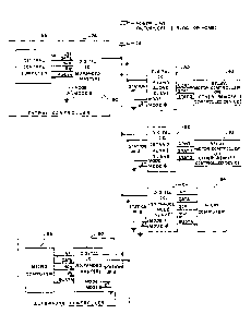
In FIG. 12 the main component parts of the
digital IC 80 are shown in block diagram form when
the device 80 is operated in the s~and alone slave
mode and 1~ ~rranged to receive a message transmitted
over the networlc 7~ which includes a shed load in-
. truction. The incoming message is amplified and
30 limited in the coupling networ~ 90, as will ~e de-
scribed in m~re detail hereinafter, and i5 applied to
the RX terminal (pin 6) of the digi'cal IC 80. It
will be understood that the incoming me~sage i a 33
bit mes~age signal having the format descri~ed in de-
35 tall heretofore in connection with Fig. 2. This in-
coming me~sage i demodulat~d in a digital demodu-
lator 150 whicn also includes the ~tart ~it d~tection
~Lz~
32 51930
and framing logic nece~sary to e~ta~lish the bit in-
terval~ of the incoming asynchronous message trans-
mitted to the device 80 over the network 7~. The
digital demodulator and its aecompanying framing
logic will be de cribed in more detail hereinafter in
connectlon with a description of the detailed ~chema-
tic diagram of the device 80 shown in FIGS. 18 to 33.
The output of the demodulator 150 i~ sup-
plied to a serial shift register indicated generally
at 152. The serial shift register 152 comprises a
series of 26 serially connected stage~ th~ fir~t 24 of
which are identified as a buffer and store bit~ ~3-
B26 tFi9. 2) o~ the received me~3age. The next ~tage
is the control ~it regi~ter U528 which ~tores the
15 control bit B2 (Fig. 2) of the re::eived message. The
final stage of the serial shift register 152 is a
start ~its registet V641 which s~ores ~its ~0 and Bl
(Fig. 2) of the received message. In this connection
it will ~e recalled that the two start bits B0 and Bl
of each message both have a logic value of al~ and
hence constitu'ce a carrier signal which extends over
two ~it interYals so that both bits may be registered
in the single reqi~ter U641. In thi~ connection it
should be not~d th~t all logic components having U
25 numbers re~er 'co th~ corresponding logic element
shown in detail in the overall schematic of the digi-
tal IC 80 hown in FIGS. 18 ~o 33. The serial shift
regi~ter 152 i3 loaded from the left by the demodu-
l~ted output of the demodul~tor 150 which i~ applied
to th~ data i~put of the register 152, this data ~e-
ing cloc~ed into th~ regi ~er 150 by means of ~uf fer
sbift clock pulseg (BS~FCLK~ developed by the demodu-
lator 150 at the end of each ~it interval in a manner
de~cribed in more detail hereinafter. Accordingly,
the incoming message i shif~ed through ~he register
:~ 152 until the start bit~ register U641 i~ set ~y the
two ~tar~ ~its B0 and ~1 to a logic "1~ value, In
~78~5~
33 51930
~hi connection it will ~e noted that the bits of the
inco~inq mes~age are stored in the ~uffer portion of
~he regi ter 152 in the manner shown in FIG. 2 with
the lea ~ significant bit ~3 stored in the register
next to the control bit register U528.
A~ the demodulated data ~its are thus ~eing
loaded into serial shift regi~er 152 tbey are also
simultan~ou~ly supplied to a BC~ error code computer
indicated generally at 154. More pasticularly, the
DEMOD output of the demodulator 150 is supplied
through a switch 156 to the input o~ the BC~ error
code computer 154 and the output of thi~ computer i~
connected to a recirculatinq input through the switch
158. The BCH error code computer 154 comp~i~e~ a
serie~ of 5 serially connected shift regi~ter stages
and when th~ switches 156 and 15~ are in the po~ition
shown in FIG. 12 ~he computer 154 computes a 5 ~it
ereor code ba~ed on the first 27 message nit3 which
it receives from the demodulator 150 as the e ~its
are being stored in the serial shift regi3ter 152.
The clock pulses on ~he BSHFCLK line, which
are u ed to advance ~he ~rial shi-ft regi ter 152,
are al~o upplied to a message bit counter 160. The
counter 160 i~ a ~ix stage counter which develops an
25 ou~pu~c on it~ end-of-word (EOW) output line when it
count~ up to 32. In this connection it will ~e
not~d ~h~t by u~ing two logic "1" start bits which
are counted ~s one, the total message length may be
counted by digital logic while providing increased
30 noi~ immun~ty ~y virtue of ~he longer s~art ~i~ in-
terval .
The message ~it counter 160 also sets a
latch al: the end of the 26th me~sage ~it and devel-
opes an enabling ~ignal on it~ GT26 (greater t~an 26)
35 output line. The GT26 ~ignal control~ ~che ~witches
156 and 158 ~o tha~c after th~ 26th m~ ge bit the
DE~OD output of the demodulator 150 i~ ~upplied to a
34 51930
BCH compara~or 162 to which comparator the output o~
the BC~ erro~ code computer 154 is also supplied. At
the ~ame time the ~witch 158 is opened by the GT 26
signal so that the BC~ error code computed in the com-
puter 154 re~ains fixed at a value corresponding tothe firs~ 26 bit~ of the received message. Since the
demodulator 150 continue~ to supply BSHFCLK pulse~ to
the computer 154, the BC~ erroc code develcped in the
compu~er 154 is then shifted out and compared ~it by
bit with the next 5 ~its o~ the received me~sage i.e.
B27-B31 ~Fig. 2) wh1ch con~ti~ute th* BCH error code
portion of the incoming received message and ar~ ~up-
pli~d to the other input of the BC~ comparator 1620
If all ~ive bits of the 8CH error code co~puted in
the computer 154 correspond with the f ive bit of the
BCH error code contained in ~its B2~-B31 of the re-
ceived mecsage the compasator 162 develops an output
on its ~CHOK output line.
The digital IC 80 also includes an address
decoder indicated generally at 164 which comprise~ a
series of 12 exclu ive OR gates and associated logic.
It will ~e recalled fro~ the previo~s description of
: FIG. 2 that ~its B11-~22 o~ a received mes~age con-
tain an address corresponding to the particular stand
alone slave with which the cen~ral controller wishes
to eommunica~e. Al~o, it will be recalled from the
preceed1ng de~cription of FIG. 10 that the address
~ele~t swit~hes 120 are connected to the addre~s pins
A0-All of the digital IC 80 in accordance with the
addre~ a~igned to each particula stand alone
sl~Ye, The addre~Y decoder 164 compares the ~etting
of the address select switche~ 120 with the address
stored in bit 811-B22 of the buffer portion of the
serial ~hift register 152. ~f the two addres~es co-
incide th~ de~oder 164 developes an outpu~ on its ad-
dre3s 0~ (~DDOK) output line.
51930
~ he digital IC ~0 also includes an instruc-
tion decoder 166 which decodes the outputc of the
buffer stages corre~ponding to bitJ B3-~6 (Fig. 2)
which contain the instruction which th~ addressed
stand alone slave i5 to execute. Assuming that ~its
B3-B5 all have a logic value of no~, a shed load in-
struction is decod~d, as shown in FIG. 3, and ~he in-
struction decoder 166 produces an output on i s shed
load line ~SHEDN).
As discussed generally heretofore, tn~ con-
~rol ~it B2 of a message intended for a ~tand alo~e
slave always ha~ a logic value of ~lw indicating that
~its ~3 B26 o~ this message include addres~ bit~ and
instruction bits which are to be compared and decoded
lS in the decoders 164, lS6 of the digital IC 80. When
the control bit register U528 in the serial shift
register 152 is set an enabling ~ignal is supplied
over the CONTROL output line o~ the register U528 to
the execute logic circuits 170. The BCHOK output
line of the comparator 162, the EOW output line of
the mes age bit counter 160 and the ADDOK output line
of the address decoder 164 are also supplied to the
execute logic circuit~ 170. Accordingly, when ~he
mes~age ~it counter 160 indicates that the end of the
message ha~ been reached, the comparator 162 indi-
cate~ that all b}t~ of the received BCH error code
agr~ed with the error code computed by the computer
154, the addre~s decoder 164 indicates ~hat the mes-
~age 1~ intended for this particular stand alone
slave, and the control bi~ register US28 i~ set, the
logic circui~s 170 develop an ou~pu~ signal on the
EXECUTE line which is anded with the SHEDN outpu~ of
the in-~truction decoder in the N~N~ gate U649 the
output of which is employed to reset a shed load
latch U651 and U6~2 so that the COUT output pin of
the dttigal IC ~0 goes to a logic value of ~0~ and
power is removed from the con~rolled devic~ 82 (Fig.
36 ~ 2S~19 30
1). The stand alone slave thus executes the instruc-
tiorl cpnt~in~d in the received me5sage to shed the
load of the controlled device 82. As discussed gen-
erally heretofore when power is applied to the digi-
5 tal IC 80 the shed load latch is ini tially reset ~ythe signal app~aring on ths PONN line ~o that the
COUT line goes high when ~5v. power is applied to ~he
device 80.
When the message ~it B6 (FigO 3) has a
10 logic value of "1" the stand alone slave not only
executes a ~hed load instruction in the manner de-
scribed in connection with ~IGo 12 but also is ar-
ranged to transmit a reply mes~age bac~ to the c~n-
tral con~roller as shown in FIG. 4. In this reply,
message bits B25 and B26 contain the two status in-
puts STATl and STAT2 which appear on pins 26 and 25,
respectively, of the digital IC ~0. Considered very
generally, this reply m~ssage is developed ~y shift-
ing out the data which has been stored in the serial
shift register 152 and employing this data to on-o~f
~ey a 115.2 kHz ~arrier which is then supplied to the
TX output pin of the device 80. HGwever, in accord-
anc~ with an impor~ant aspect of the disclosed
system, the statu~ signals appearing on the STAT 1
25 and STAT 2 input pins of the device 80, which repre-
sent the condition of the controlled relay, are no~
emplayed to set the status bits B~5 and B26 of the
reply me sage until a~ter 15 bit~ have been read out
of the ~erial shift regi~ter 152. This gives consid-
30 erabl~ time for the ~elay contacts to se~'cle down ~e-
fore their ~tatus is added ~o the reply message being
transmitted ~ack ~o the central con~roller.
I~ F1g. 13 the operation of the ~tand alone
~lave in formatting and transmitting ~uch a reply
me~s~ge ~ack to the central con~roller i~ shown in
block diagram form. R~ferring to thi~ figure, it i~
a~sumed that a message ha~ b~en re~eived f rom the
~7~S9
37 51g30
c~ntral co~troller and has been 5t~red in the serial
shlft register 152 in the manner descri~ed in detail
bergtofore in connection with Fig. 12. It i~ ~urther
a~umed that the control bit B2 of the rec~ived mes-
~ag~ has a logic value of nl~ and that the messagebit B6 stored in the ~uffer portion of th@ register
152 has a logic value ~1~ which instructs the stand
alone slave to transmit a reply meRsage ~ack to the
central controller. When ~he B6 ~it has a "1~ value
the in~truction decoder 166 produces an output ~ignal
on itq COM 3 output line. Also, at the end of the
recelved message the execute logic circuits 170 l~ee
Fig. 12) produce an EXECUTE ~gnal when the condi-
tion descriDed in detail heretofore in connection
with Fig. 12 occur. When an EXECUTE signal i~ pro-
duced a reply latc~ 172 provide3 an output which i5
employed to set a s~atus latch 174. The status latc.h
174 provldes a control signal to the status control
logic 176. However, the condition of the ~ta~us pin~
STAT 1 and ST~T 2 is not employed to set correspond-
ing stages of the buffer pDrtion of the serial shift
regi~ter 152 until after 15 ~its have ~een shifted
out of tbe register 152. At that ti~e the me~sage
bit cou~ter 160 provides ~n ou~put on its "15~ output
line whi~h is employed in the status con~rol logic
176 to ~et the corresponding stages Or ~he ~uffer
portion o~ the regi~er 152, ~hese stage correspond
ing to the location of bits B25 and B26 in the reply
~es3ag~ after 15 bit have been shifted out of ~he
r~gi~ter 152.
Con~idering now the manner in which the re-
ceived me~sage which ha~ been stored in the serial
shift regis~er 152 i5 shifted out to form a reply
~e~age, it will ~e re~alled that a me~age which is
tran~mitted over the network 78 require~ two start
bit3 having a logic value sf ~ owever, wh~n the
mes~age was received i~ was initially detected by de-
38 51930
~ecting the pre ~nce of carrier on the network 7~ ~or
a dura~ion o~ 2 bits and, hence, the two start bits
of the received m~ age are stored as a single ~it in
the ~tart bit~ register U641. When a reply mescage
i~ to be tran~mitted over the networ~ it is necessary
to provide a modulated carrier of two ~itC duration
in re~po~se to the single start ~it stored in the re-
gi~ter U641. To accomplish thi , a tran~mit strobe
signal ~TXST~) i3 derived from the reply latcb 172
and is coupled through the N3R ga~e U601 to reset a
one ~it delay fl~p-flop 178 whicb ~as it~ D inpu~
connected to the five volt supply Vdd. As a re-~ult
the QN output o~ the flip flop 178 i~ inverted to
provid~ a transmit stro~e A tTXSTBA) signal which
se~s a transmi~ con~rol latch 180~ When ~he latch
180 i~ et it provides a tran mit on (TXO~N~ signal
which is employed ~o relea~e the framing counter in
the demodulator 150 so that they ~egin to provide
BSHFCL~ pulse~ at one bit intervals.
For the first 26 ~it~ of ~he reply message
th~ output of the ~tart bi~ register U641 is con-
nected throuigh a ~witch 190 to a ~-rans~it flip-flop
182 which 1~ al~o set ~y the TXSTB~ ~ignal and is
held in a ~et cond~tion qo that it does not respond
to the fir~t BSH~CLR pul~e which is applied to its
clo~k $nput. At the ~ame time the QN output of the
one bit del~y flip-flop 17S i~ com~i~ed with the
f ir~t BS~FC~ puls~ in the NAND g3te U668 so as to
provide a ~gnal which ~et~ a transmit enable latch
18~. When ~he ~ransmit ena~le latch l~ is set it
provide~ an enabling ~ignal to the modulator 186 to
which is al30 supplied a ~arsier signal having a fre-
quency of 115.2 ~z. from the digital demodulator
150. When the tran~mit flip flop 1~2 is initially
set by the TXST~ line going low, it provides a 1 on
it-~ Q output ~o the modula~or 186. Accordingly, when
the ~rans~it ena~le latch 1~4 provide~ an ena~ g
39 51930
3ignal to the modulator 186 a carrier output i5 SUp-
plied to the TX output pin of the device 80 and is
suppli~d to the networ~ 7B. During this initial
transmi~ion of carrier during ~he first start bit
interval the data in the serial shift register 152 is
not hifted out ~ecause 8SHFCLX pulse~ to the cloc~
input of the register 152 are ~locked by the ~AND
gate U697. The NAN~ gate U697 ha~ as its second input
a signal from the GT26N ou~put line of the ~es~age ~it
counter 160 which i~ high until 26 ~its h~ve been
shifted out o~ the register 152. However, a th~rd
input to the NAND gate V697 i~ the TXSTBA line which
went low when the 1 bit delay flip-flop 178 wa~ re-
set. Accordingly, the first BS~FCLR pulse i~ not ap-
plied to the cloc~ input of the regl~ter 152 al~houghthis pulse does set the trans~it ENAB~E latch 184 and
enable carrier output to be suppli~d to the TX output
pin for the first bit interval. ~owever, a ~ho~t in-
terval after the first BSHFCLK pulse, a delayed shift
20 cloc~ pulse (DSHFHCLK), which is also developed in
the framing logic of the dem~dulator 150, i~ supplied
to ~he clock input of the 1 ~it d~;ay flip-flop 178
so 'chat the TXSTBA line goes high shortly a~ter the
~ir~t 8SHECLR pulse occur~. When the TXS'rBA line
25 goe~ high the BSHEY:LR pulses pa~s through the NAND
gate U697 and shif t data out of the register 152 and
'che ~e~l~lly connected trarlsmit ~lip-flop 1~2 to the
modulator 186 ~o that the ~ gle tart ~it ~ored in
the regi~ter U641 and the remaining ~it~ B2-B26 Of
30 the reG~ived message con~rol the modulation of the
carr~ er supplied to th~ 'rx outpu~ pin. In thi~
connection it will be noted 'cha'c th~ BSHFCLR pulses
are al30 ~upplied 'co the clock input of th~ trarl~mit
flip-flop 182 ~o a to permit the ~rial shiflt of
35 da~ca to the TX ou~cpu~ pin. However, a3 di~cus~ed
~b~ve, when the TXSTaA llne i~ low 1~ hold~ ~he flip-
~0 5 l9 30
~lop 18~ set so that it does no'c respond to the f irstBSHFCLR pulse.
Considering now the man..er in which the
STAT 1 and STAT 2 status signals from the controlled
device are ad~ed to the reply message, it will be re-
called that the ~uffer stag~s are not set in accord-
ance wi~h the signals on the STAT 1 and STA~ 2 pins
until 1~ ~its have ~een ~ni~ted out of the regiseer
152 in order to allow time for the relay contacts of
the controlled device to assume a final position. It
will also be recalled that the B25 and B26 bit~ of
the received message are reserved for status ~its to
be added in a reply message so that the last active
bit in the received mes age is ~24. When the B24 bit
has been shifted 15 times it appears in the B9 stage
of the buffer portion of the erial shift register
152. Accordingly, the conditions of the tatus pins
STAT 1 and STAT 2 can be set into the B10 and Bll
~tages of the buffer after the 15th shift of data in
the regis~er 152. To this end, the mes~age bit
coun~er 160 develops a signal on the ~15~ output line
which is sent to the status control~logic 176. This
logic was ~na~led when the status latch 174 was set
in respon~e to a CO~ 3 siqnal inàicating ~hat the
25 reply was request~d. Accordingly, tne status control
logic then re pc>nds to the "15" sig~al by setting
th~ BlO a~d E~ tage~ in ac~ordance with ~he poten-
ials on the Sq~AT 1 and STAT 2 pins. In this connec-
tion it will be under~tood thae the B10 and Bll
39 ~tage~ of th~ buf fer initially contained part of the
addre~ in the rec~ived m~ssage. However, after the
receiv~d message has been shifted 15 bits during
transmi~sion of the r~ply message the stages BlO and
~11 are f r~e to ~e set in accordance with the s~a~cus
pin~ STAT 1 and STAT 2 and thls statu-~ will be t~ans~
mitted out as a part of ehe r~ply mes age in tbe ~25
and ~26 bit po~itions.
~1 51930
A~ discussed generally heretofore, it i5
neoe~ ry to compute a new BCH erro~ code for the re-
ply meQsage which is transmitted back to the central
controll~r du~ to the fact that the status bits B25
and B26 may now contain status information whe~e ~hey
were not used in the received ~eScage. ~ soon as
the transmit control latch 1 0 i5 set the TXONN sig-
nal controls a switch U758 so that th~ D~MOD output
of the demodula~or 50 i9 removed from the data input
of the BC~ error code computer lS4 and the ouptut of.
the serial shift register 152 i~ connQcted to this
input through the switch 156. ~owever, during the
initial 1 ~it delay of the flip flop 178 BS~FC~R
pulses are blocked from the cloc~ input of the com-
parator 154 ~y the NAND gate U672 the other input of
which is the TXSTBA line which i~ low for th~ first
start ~it. After the first BS~FCLR pulse tbe TXSTBA
line goes high and succeeding BSHFCLK pulses are 3up-
plied to the computer 154. The two ~tart ~its of the
transmitt~d message are thu~ treated a~ one ~it ~y
the computer 154 in the same ~anner as the two start
bittivs of a received message are dec~ded as one ~it for
the register U641.
As the data stored in the regi~ter 152 is
shifted ou~ to the transmit flip-flop 182, this data
is also supplied to the data input of th~ ~CH error
oode computer 154 through the switch 15fi. Also, the
recirculat~g input of the compu~er 154 is connected
through the swiech 158, as descri~ed here~ofore in
connection ~ith Fig. 12. Ac~ordingly, a~ the 26
~it~ ~tored in the register 152 are shifted out of
thi~ register, the computer 154 is computing a new
BC~ erro~ code which will ta~e into account the
status information in bi~ B25 and ~26 thereof.
After the 26th bit ha3 been 3hifted out of the reg~s-
ter 152 a new five bit error code i~ th~n pre~ent in
the co~puter 154. When the mes~a~e bi~ counter 160
42 519 30
produce~ an output on the ~T26 line the switches 156
ahd 158 ar~ opened while at the ~ame time the output
of t~e compu~er 154 is connected through the switch
190 to ~che lnpu~ of the transmit flip-flop 182 in
S place of the output f~om the ~erial shift register
152. Since B5E~CLR puls~c~ are ~till applied to both
the BCH er~or code computer 154 and the transmit
flip-flop 182 the five ~it error code developed in
the computer 154 is succes~ively cloc~ed throu~h the
transmit flip-flop 182 to th~ modulator 186 so a~ to
con~titute the BCE~ error code portion of tbe trans-
mitted reply messag~.
When the switch 156 i~ opened af t~r the
26th bit, a zero is applied to the data input of the
BCH error code computer 154 30 that as the f ive ~it
error code is shifted out of the BCH error code
computer 154 the shift regi~ter stage~ are bac~
f illed with zeroe After th~ f ive error cod~ bits
have been shi f tedl out, ~he next BS~FCLK pul~e clocks a
zero out of t~e compulter 154 and 'chrough the l:ransmi~c
flip-flop 182 to the modulator 186 to corl~titut~ the
~32 top bi'c which ha~ a logic va~ue of " 9" . This
comple~e~ tran~mis ion of the 33 bit me~age on~co the
networ k 7 R .
When the me~sage counl:er 160 has counted to
32 bit~ it~ EO~7 line i9 supplied to a "ran~it of f
flip flop 192 so th~t a transmi~ off signal (TXOFFN)
i~ dev~loped by the flip-flop 192. The TXO~FN signal
i~ e~oployed to re~et the ~ta~cu~ latch 174 and tne
tr~n~mlS control latch 180. Wherl the transmit
control latch 180 i ~ re~et it~ $XONN ou'cput line re-
~t3 the tran~mit ~NABLE latch 184~ The reply latch
172 iR r~et by timing pUlSe3 STBAD developed in the
fra~ing logic of th~ de~odulator 150, ~ w~ e
d~cribed in more detail her~inafter.
~;~7~
'~3 51930
~x anded Slave Mode
b
In Fig. 14 there is shown a block diagram
o the digital IC 80 when operated in an expande
slave mode and showing the operation of the device 80
5 in r~pon~e ~o an enable inter~ace instruction. It
will b~ rec~ d from the previous de~cription that
in 'ch~ expanded mode, pin 24 (DATA~ o~ th~ di~i'cal IC
is used as a bi-directional ~r ial data line by mean
of wh$ch data stored in th~ serial Yhift register 152
10 may be read out by an assbciated ~icrocomputer, ~uch
a~ ~he microcomputer 84 ~Fig. 1), or data from the
mi crocomputer can be loaded into the r~gi~ter 152 .
Also, pin 26 of the device 80 ~ct~ a~ a ~erial clock
(SCg) input by means of which erial cloclt pul~es
15 supplied from the associatea microcomputer 8~ may ~e
connec~ced to th~ cloc~ input of the r@gi5t~r 152 to
control the ~hift of data fro~n thi~ register onto t~ e
data output pin 24 or the cloc~ing of dat~ pla~ed on
'che DATA pin into the register 152. Also, pin 2~ of
20 the device 80 ~RW) is connected as a read-write
control line wbich may be controlled by the
a~soci~ted microcomputer 84 to co~ltrol eith2r the
reading of data from the regist~ 152 or the writing
of data in~o thi~ regi~ter from the microcomputer ~40
25 The RW line is also used by ~che microcomputec 84 to
force the digit~l IC 80 to ~ran . mit the data presen~
in i~ regi3ter lS2 onto 'che network 7B ir th~ 33 ~it
~e~age forn~at of thi~ network~ Pin 9 of the device
80 function~ a~ an interrupt line (INT~ to the
30 la~croce~puter 84 in the expanded mo~e and ~upplies an
inter~upt ~ignal in respons~ to an ena~1~ $nterface
in~truction which informs the micro 84 that a m~s~age
intend~d or lt ha~ ~een s~cored in the r~gl~t~r 152.
An inte~upt ~ignal i~ al30 produced on the INT line
35 afer the devlce 80 ~a~ tran~mitted da'ca lo~d~d into
the reg~ t~r 152 onto the networkl, P~n 8 of the d~-
vice 80 Ruppli~s a busy ~ignal (BUSY~) to the a~so-
1~!~3
44 51930
cia~ed ~icro 84 whenever a mes5age is being received
by the.device 80 or a me~sage is bei~g transmitted ~y
thi~ devlce onto the network 78.
It will ~e understood that the block dia-
gram of Fig, 14 ~ncluda only the circuit component
and logio ga~e~ which are involved in ~etting up an
interface with the a~ociated micro 84 and th~ bi-
direc~ion~l trans~ission of data and control ~ignals
between the micro 84 and the device 80. In Fig. 14
it is assumed that a mes~age has been rece~ved ~rom
the cent~al cont~oller which cont inR an instruction
to establish an interface ~i~h the as~ociated micrv~
computer 84 in bit3 ~3-BS of the-me~age and that the
instruction decoder 166 has deooded thi~ instruction
~y producing an output on it~ enable interface output
line ~EINTN). Also, when the device 80 i op~rating
in a~ expanded lave mode pins 1 and 27 are grounded
and the expanded mode line EMN is high.
In the expanded mode of opsration o~ the
digital device 80, a serial statu3 r~gi~ter 200 i~
employed wbich include~ a BCH error registe~ U642 and
an RX/TX regi~er U644. The ~CH er~o~ regi~t~r U642
i5 serially connected to the output of th~ control
~it regi~ter U52B in the seri~l snift regist2r 152
ov~r the CONTROL li~e. The RX~TX register V644 is
serially conn~cted to the output of ~he BCH error re-
gi3ter U542 and the output of the regi~ter 644 i5
~upplled throug~ ~n inverting tri-state ou put clrcuit
U762 to the bi-directional serial DATA pin 24.
~ 30 I~ will be recalled fro~ the previou~ di~
cu~lon of Fig. 12 th~t when the digital device 80
recsives a me~sage ~rcm the centr~l con~roller which
includa~ an instruction it will not execute that in-
struction unless the BCH comparator 162 lFig. 12~
provid~ a BCHOK output whlch indicates th~t ~ach bit
o~ the BC~ error oode ~n the re~e$ved m~ g~ co~-
pare~ equally with the BCH error cod~ ~o~put~d ln the
~ ~7 ~5 3
51930
device 80. The BC8 error register U642 is ~et or re-
~t in . accord3nce with the BCHOR output from the BCH
comparator 162. The BCH error regi;ter U64~ is reset
wh~n the init~al me~ag~ i8 receiv~d reql~es'cing ~hat
5 the in~;erface b~ established ~ecau~e this in3truction
would not have been ex~cu~d if it wa~ not error-
free. However, once this interface has ~een set up
the central controller may send additional mesqages
to the microcompuSer 84. l:uring receipt of each of
10 the e additional messag*s the E~CH co~parator 162 com-
pare~ the E3C~ error code cont ined in the c~ceived
mes~age with the 3CH erro~ code comput~d ~y the com
puter lS4 and will indicate an e~ror ~y bolding ~che
BCHOK line low if all ~ of the two codes are not
15 the same. If the BC~OK line is low the BC~ error
registe~ IJ642 i~ set. Howeves, ~ince the interfac~
has already ~een set up, this second me~age tored
in the regie~ter 152, which contains an error, may
read out by the microco;nputer 84 ~y succes~ively
20 clocking the SCK line and reading the DATA line. I'he
pre~ence of a logic "1" in the BCH error register
po ition ~cond ~it) of the data- read olat ~y 'che
microcomputer 84 indica~e~ to the microcompu~er 84
that an error in tran~mi~sion has occurred and that
25 the microco~pu~r may wiqh to as~ the central con-
l:roller ~ repeat the m@~age.
~ rh~ RX~TX regi 'c2r U 64~ is ~mployed to in-
dic~te to ~h~ mlGrocomputer 8~ whether or not the
~e2ri~1 ~bift regi3ter 152 i~ lo~ded or empty when it
30 recel~ an interrupt signal on the INT lin@. If the
regi~ter 152 ha~ been load~d with a received me~sage
~rolR th~ central con~roller ~che RX/TX register U644
~ e~. When the micro re~d ou~: the dat3 ~tor~d in
the regi~ter 152, ~h~ serial shif~ register lS~ and
35 the ~erial statu regiYter 200 ~re bac~t f illed ~ h
zeroe~ ~o that when ~he readout i~ complet~ly ~ zero
will ~e stored in the RX/TX ragi~ter U644. Whan data
~7~
46 ~1930
i~ then loaded into the register 152 and tran~mitted
out to the network this ~ero remai~s stored in the
RX/TX register since it is not used during transmis-
Rion. Accordingly, when an interrupt is produced on
the INT lin~ after the message is transmitted, the
RX/TX r~gi~er U644 remain~ at zero o as to the in-
dicate to thQ microcomputer that the message ha3 been
sent and the r2gi~ter 152 i~ empty.
When the digital IC 80 i~ arranged to re-
ceive a me~sage from the network 78, the ~witches
U759 and U760 have the po~ition ~hown in Fig. 14 ~o
that the output of the demodulator 150 ls ~uppli~d to
the data input of the serial shift regi~ter 15~ and
the received message may ~e clocked into regi~ter 152
~y mean~ of the BS~FC~K pul~es applied to the cloc~
input uf the register 152. However, as soon a~ an
enable interf ace command has been executed in the IC
80 control of the register 152 switches to the a so
ciated microcomputer 84 by actuating the ~witches
U759 and U?60 to the opposite po ition. Thi~ insures
that data which ha~ ~een stored in the regisSer 152
during the r~ceived message is preserve~ for tran~-
mi~ ion to the microcomputer ~4. It is important to
switch control of the regis~er 1~2 to the microcompu-
~er 84 immedia~ely because the micro might not be
a~le to re~pond immediately to its interrupt on the
INT line and an lncoming message might write over the
d~ta in the register 152 before ~he micro reads out
thl~ d~ta.
- 30 Wbil~ the int2rface is esta~lished to the
microcomputer 84 no more network transmi~io~ will
~e demodulated and placed in ~he serial shift regis-
t~r 152 until the microco~puter 84 relinqui3he~ con-
trol. Howev~r, after oontrol i~ hifted to the
microco~puter 84, the digi~al demodula~or 150 conti-
nue~ ~o demodulate network mes~ages and when ~ net-
wor~ mes age is received produc~s ~ signal on its
~;~7~5.~
47 51930
RXWDETN s)utput line. This ~ignal i5 transmitted
t~rough th~ NP.ND gate U671. The o~ltput of the NAND
9~t~ U671 is inverted to produce a BUSYN output
sign~l to the ~550ciat . d microcomputer 84 . The
5 MiCrOCOmplJt*r 84 iS thus informed that the device 80
ha~ dete~ted ~ctivity on the networ~ 78. This
ac$ivity migh~c ~e that the central controller is at-
temptir,g to communicate with th~ microcomput~r
through the ena~led slave mode digital IC 80. When
10 the digital IC ~0 i9 transmitting a message back to
the central controlle- over the networ~, as de cri~e~
heretofore, the TXONN ~ignal developed ~y th~ tr~ns-
mit control latch 180 (Fig. 13) al o ~uppli~s an ac-
tive low sigr~al to the Busy~a output pin to in~orm the
15 microcomputer 84 tnat a me sage is being transmitted
by the digital IC 80 to the central controller over
the ne twor k ~ 8 .
Considering now in more detail the manner
in which control of the regi~ter 152 is shifted from
20 the n~two~k to the microcomputer 84, when the ena~le
interfac@ command is decoded by tbe instruction de-
coder 166 it produce an EINTN ou~u~c which se~s an
ena~le interface latch 202. The low output of the
latch 202 i~ co~bined with ~he master slave signal
25 EMN, which is high in the expanded slaYe mode, in the
MAND gate U749 c- a3 to provide an active high signal
on the ENA3~LlS output of the NAND gate U749 which is
one input of the NAND gate U686. A ~ning that 'che
oth~r inpug o~ the NAND gate U686 is al50 a 1, the
30 outpue of US86 goes low which i~ inver~ed in ~he in-
verter U736 ~o ~hat the UPSi~N line goe~ high. The
UPSLN lin~ is employed to control the switches U75~
and V760 and when it i~ high switches th~ data input
of the regis~er 152 to the ~i-direetional ~erial DP~TA
35 lin~ through invel ter U547 and the cloc~ input of the
regi~ter 15~ to ~he seri~l cloc~ SCR lineO More p~r-
ticularly, the UPSLN line directly con~rols switch
48 51930
U760 3c: th~t the SCX serial clock line is connected
l:O the cloc~ input of th@ regi~ter 152~ Also, the ~5
UPSL~3 line through the inverter U547 is one inpu~ of
the ~OR ga1:e U597 the other input of which is the RW
5 line which is normally high due to an internal pull
up re3is~ r in ~he digital IC 80. Accordingly, a
high orl the UPSLN line cau~es the switch U75~ to dis-
connect the demod output of the modula~cor 150 from
the data input of the regl~tec 152 only when the RW
10 line is low.
When the microcomputer 84 wishe~ to read
the data ~tored in the serial ~hift register 152 it
does ~o ~y providing serial cloc~ pul~es to the SCX
line. At the same l:ime the ~W line i~ high which
15 controls the tri-state output circuit U762 to corlnect
the output of the RX/TX register V644 to ~he ~i-
di r ect ional DATA l i ne . Accor di ngly th e DATA pin wi ll
contain the ~kate of the RX/TX regicter U7644 which
e~n ~e read by the microcomputer 84. When the UPSLN
20 line i~ high and the RW line i~ also high the output
of the NAND gate U683 i~ low wh~ch is inverted by the
inverter U~00 and applied as one input to the NAND
gate U801 the other input o~ which is the SCR line.
The output of th~ NAND gate U~01 is inverted ~y
25 inverter U802 and i5 supplied to the clock irlputs of
the BC}~ ~ror r~gi~ter U642 and th0 RX/TX regis'cer
U644 ~o th~t the~e registers are also shifted ~y
pul~e~ produced by ~he micro on the SCE~ lin~.
Accordirlgly, when the micro clocks the SCR pin once
30 all of the data in the serial shift register 152 and
the ~erlally connected 3erial tatu3 register ~00 is
~hifted to the right SQ that ~he sta~e of the BCH er-
ror register U642 will b~2 present a~ the DATA pin.
The T~icro c~n ~hen read the DATA pin again to o~tain
35 the . tate of thl~ register. Th~ clocking and read-
ing proce~s continue~ until tSle ~icro ha~ r~ad out of
the DATA pin all of the dat~ in tbe ~rial ~hift
49 51930 ~
regi~ter 152 and the serial status register 200. In
~hi~ connection it will be noted that the start bit
regi~t~ U641 is ~ypassed during the readout opera-
tion ~ince it~ information is used only in transmi~-
ting a message to the network. As indicated a~ove,the stages of the cerial s~atu~ register 200 are in-
cluded in the chain of data which may ~e shifted out
to the microcomputer 84 becau~e these stages contain
information which is useful to the microcomputer ~4.
It will also ~e noted that when an ena~le
inter~ace signal is produced and the UPSLN line is
high, the RW line is also high wh$ch produce~ a zero
on the output of U683. The fact that both th~ UPSLN
line and the RW line are high forces switch U759 to
the DEMOD position. However, 3ince the output o~
U683 is low the data input to the serial shift r~gis-
t~r lS2 will always ~é logic zeros. Accordingly, as
data is ~eing read out of the register U644 on tbe
DArA pin 24 the register 152 and the serial ~tatus
register 200 are being ~ac~ filled with zeros. After
the entire con~ents of these regist2rs ha~ ~een read
out ~he RX/TX register U644 contain~ a zero so that a
zero appears on the DATA pin thereafter. ~s i~dicat-
ed a~ove, when the micro receiYes a second interrupt
on the INT line after a message has been transmi~ted
the micro can read the DAT~ pin and verify that the
: ~e~s~ge has ~een ent.
Con idering now the manner in which the
se~g~ of the ~erial status register 200 are set at
th2 end of either a received mes~ag~ or a transmitted
m~sage to provide the a~ove-de~cribed information to
the micro, at th~ end of a received m~sage the mes-
sage bit counter 160 (Fig. 12) produce~ ~n ~OW 9ig-
~al whlch is co~ined with DS~FCLR pulses from the
digi~al demodula~r 150 in the NAND gate U~7 ~Fig.
14) to provide a statu~ trobe ~ignal STSTB. The
: STSTB signal is com~ined with the ~CHOK ~ignal in the
50 51930
NAND gate U660 so that the BCH error regi ter U642 is
reset i the r~ceived message was error free. The
BC~OR signal is inverted in the inverter U555 whos
output is also com~ined with the STSTB signal in the
NAND ga~e U65~ so that the ~CH error registe~ U642 is
set if there was an error in the received message.
The STSTB signal is also comDined with the E~ABLE
signal in the NAND gate U658 the output of which is
supplied to one input of a NAND ga~e U756 the other
input of which is the TXONN line which is high when
the device 80 is not transmitting a me~age. Accor-
dingly, the RX/TX registee U644 is s~t at the end of
a received message.
When the device ao transmits a message to
-15 the network the TXONN line is low so that at the end
of such transmission the STSTB signal does not set
the register U644. ~owever, as indicated a~ove, ~he
register U644 is ~ac~ filled with a zero as data is
read out o~ the register 152. ~ccordinglyO the micro
can read the DATA pin, to which the ou~put of the
regi~tar U644 is connected, and de~ermine that a mes-
sage has been transmitted to ~he- network and the
register 152 is empty. The register U644 is rese~
w~en power is applied to the device ~0 and when the
interface is disa~lad and the ENABLE signal disap-
pear~. Th~s reset i~ accomplished through the ~IAND
gate U657 and inverter U725 which togethe~ acl: as an
AND gate the inputs of which are the PONN signal
and the ~NABLE s ignal .
After the micro has read out 'che data stor-
ed in the serial shift reg1ster 152 and the status
regis'cer 200 it can either switch control ~ack 'co the
: networi~ immediately or it can load data into the ser-
ial ~hif'c regisi:er 152 and then command the device 80
to ~ransmiS the data loaded into the regi~ter 152 on
to the network in a 33 bit ~e~age having ~he aDove
descri~ed network ~ormat. The micro switcbe~ control
~Z~
51 51930
back to the netwoek im~ediately by pulling the RW
li~e low and the~ high. However, the low to high
transition on the RW lin~, which is performe~ ~y the
microco~puter 84, occurs a ynchronously with respect
~o the framing logic in the demodulator 150. Accor-
dingly, i~ is impor~ant to make sure that the device
80 sees the zero ~o one transition which the micro-
computer 84 places on the RW line, This transition
is detected by a digital one ho~ 204 the two stages
of which are clocked ~y the STBDD timing pulse~ from
the framing logic in the demodulator 150. The ~tages
of the one shot 204 are re~et ~y the RW line so that
during the period when the RW line i~ held l~w by the
microcomputer 84 the output line RWR of the one shot
204 remains high. However, upon the ze~o to one
transition on the RW line the digital one shot 204 is
permitted to respond to the ST~DD pul~es and produces
an output pulse o~ the RWR line of guarante~d minimum
pulse width due to the fact that it is derived from
the framing logic timing pulses in the demodulator
150. T~e RWR line thus goes low for a fixed interval
of time in re~ponse to a zero to bne transition on
the RW line.
When the RWR line goes low it sets a buffer
control latch 206 the outpu~ of which is connected to
one input of th~ NAND ga~e U753. The other input of
the ~AN~ ga~ i5 the RW line. Accordingly, after the
zero to 1 ~ran~ition on the RW line this line is high
~o that the output of th~ NAND ga~e U753 is no longer
a ~ nd the UP5LN line goes from high to low. When
tbis occurs the ~witches ~759 and U760 are returned
to the position~ shown in Fig. 14 so that ~uffer con-
trol t~ shifted fr~m the micro ~ack to the networ~.
Con ideri~g now the situation where the
micro wi~he~ to load data into the 3erial shift
regi3ter 152 and then command ~h~ device 80 to ~rans
mit ~he da~a in the regi~ter 1S2 onto the networ~,
52 519 30
~he micro f irst pu115 the R~7 line low which ena~les
data to ~e transmitted from th~ DATA line through the
NOR gate U5~3, the ~wltch U75~, the NAND gate U~2
and the lnverter U730 to the data input of 'che regis-
5 ter 152. A~ sta~ced previou~ly, a high on the UPSLNline has also caused th~ switch U760 /:o connect the
SCK serial clock line to the clock input o~ the
register 152 . Data f rom the micro may now be placed
on the DATA pin and clocked in~o th~ register 152 by
10 the positive clock edge~ of the SCK clock pulses.
The data entering the regi~ter 152 begin~ with a
control bi~ having a logic value of "0~ ~ollowed ~y
the least significant bit of the ~uffer b~it~ B3 826
and enda up wieh the most signif icant bit of the
lS ~uffer bits. It should ~e no~ed that the micro does
not load the s~art ~its regis~er U641.
After this data has been lo~ded into the
register 152 the micro pulls the RW pin higb. The
low to high transition on the ~W line af ~er SCK
20 pulses have ~een supplied to the SCK line is inter-
preted ~y the device 8û as meaning that data ha~ been
loaded into the register 152 and- ~;hat this data
should now be tran~mitt~d ou~ to the networ~ in the
33 ~it messag~ form~t of the networ~. To detect this
25 condition a transmit detect 1ip f lop 20~ i~ employ-
ed. Ms~re particularly, th~ cloc~ pulses developed on
the SCK line ~y the microcomputer 84, identified as
BSlSRCR pul~e~ are applied to the cloc~ input of the
flip-flop 208 and the RW line i~ connected to its D
30 input. When ~he RW line is low and a BSERCR pulse is
tran~mitted over the SCK line from 'che microcomputer
84 the Q outpu~c line of the flip-flop 208 goes low.
This output i5 supplied to the NOR gate U628 the
other input o~ which i~ ~he RWR 1 ine . Ac~ordingly,
35 when the RW lire is again pulL~d hi~h at the end of
trarl~mi~sisn of data into the regl~te~ 152 the RWR
line goss low so tha~c the output of the NOR gate U628
53 51930 ~ ~ 7
goe~ high~ Thi~ output is supplied as one input to a
N~R gate U601 and pas~es through this gat~ so as to
provide a low on the TXSTB line. A low on the TXSTB
line cause~ ~he device 80 to transmit the data stored
in the serial ~hift register 152 onto the network in
the 33 bit n~twork format in ~xactly the same manner
as descri~ed in detail here~ofore in conn~c~ion with
Fig. 13 wherein the device 80 ~ransmitted a reply
message bac~ to the central controller. However,
since the micro does not load da~a into the start
bits regis~er U641, it is neces-~ary to set this
regi ter before message is transmitted. Thi~ i.
accompli3hed ~y the TXSTBA lin~ which goes low at the
beginning of a transmitted message and sets the
registe~ ~t2ge U641 as shown in Fig. 13.
Accordingly, when the TXSTBA line goe~ high at the
end of the 1 ~it delay provided Dy the flip-flop 178,
the start bits register U641 is set and its logic X1~
can ~e shii~ted out to ~orm the second half of the two
~it start signal of the tran~mitted message as
describ~d previously.
~ hen the transmit ena~le latch 1~4 (Fig.
133 is ~et at the start of transmission of this m~s-
sage, th~ output of the NAND gate U66~ (Fig. 13) is
25 employed ~o ~e'~ the transmit de~ec'c flip flop 20~
through the NAND gate U664 the other inputs of which
ar~ the ~ower on Yignal PONN and the ENABLE signal.
When an STSTE; ~ignal is produced at the end of this
transmitted me~sage in re ponse to the delayed clock
30 pul~ DSHFCLK the TXONN line is low so that the out-
p~t of a NAND gate U687, to which these ~wo signal3
are input~ced, remains high leavin~ the ~uf fer control
latch 2û6 set. Thi~ mean3 that buf fer control, whict
was switched ~o ~he network at the ~eginning of trans-
mi ~ion, re~ains that way.
In order to signal the a~sociated microcompu~er 84 that an in~erface is ~eing ~et up ~etween
~7E~5~
54 51930
the expanded slave mode device 80 and the micro so
that ~wo-way data tran5mi~sion over the networ~ is
po~sible, the device 80 produces a high on the INT
pin 9 as ~oon as an ena~le interface instruction is
s decoded ~y th~ decoder 166. More par'cicularly, when
the RX/TX regis~er U644 i~ set at the end o a re-
ceived message containing the enable interf a~e in-
struction, as descri~ed previously, the output of the
NAND gate U756 is supplied as one inpu~c to the NAND
gate U10Qû 'che other input of which i~ 'che TXONN
line. Since the TXON~ lin~ i~ high exc~pt during
transmission a clock pulse is supplied to the int~r-
rupt flip-flop 210, al~o identified as U643. The D
line of the ~lip-~lop 210 i connected to the 5 volt
supply so ~chat when this flip-flop receiv~s a cloclt
pulse its QN output qoes low, which i inverted and
supplied to the INT pin 9 of the device 80. This
signals the associated microcomputer that an intsr-
face has ~een esta~lished ~etween it and the expanded
slave device 80 so tha~ the micro may read the d~t~
s~cored in the serial shift register 152 from the DATA
pin and load data into this regi~ter in the ~anner
described in detail heretofore. As ~oon aa the micro
produces the f irst pulse on ~he SCK line, either in
reading data ~rom ttl~ regist~r 152 or writing data
ir.to the rsgister 152, this SCR pulse re3e'cs the
interrupt flip ~lop 210 and remove~ the irl'cerrup'c
sign~l ~rom the INT lirl~. More particularly, this
SCR pul~e is supplied to one input of a NOR gate
U1002 th~ other input of which is the outpu~ of a
~lAND gate U657. The output of the NAND g~te U651 is
high when the in~cerface is ena~led and power is on
t:he device 80 so the f ir t SC~ pulse re~et~ the in-
terrupt f lip f lop 21Qo
If the micro loads the 3erial ~hift regi~-
ter 152 and ins~ruc'cs the expand~d ~lave device 80 to
transmit this message ~ack to the networ~ the TXONN
51930 i27E~
lin~ goe~ low durin~ such transmission, as described
in detail here~oore in connection with Fig. 13.
During such transmission the NAND gates U756 and
U1000 are blocked so that th~ RX/TX register U644 is
no~ 3et at the end of ~he transmi~ed message. How-
ever, when the TXONN line goes high a~ain after the
message ha~ been ~ransmitted ~he interrupt flip flop
210 is again cloc~ed so that a signal is produced on
the INT pin thus signalling the micro that transmis-
sion of a message ~ac~ to the central controller hasbeen completed. The ~aet that transmis3ion ba~ been
completed can be verified by the micro by reading the
DATA pin which is tied to the output of the RX/TX
. register U644 and would show a wO~ stored in this re-
gister. In this connection it will be noted ehat the
micro can read the DATA pin any time that ~he RW line
i5 high to enable the tristate output U762, even
though control of the register 152 has been shifted
back to ~he network. Cloc~ing of the interrupt flip-
flop 210 is timed to coincide with the trailing edgeof ~he ~USYN signal on pin 9 80 tha~ the INT line goes
higb at the ~ame time that the BUSYN-line goes high.
While th microcomputer 84 may be program-
med in any ~uita~le manner ~o receive data from and
25 transmit data to the expanded mode slave digital IC
80, in FIG. 15 there is shown a general or high level
flow chart for the microcomputer ~4 ~y means of which
it may re~pond to the interface and estahlish bi-
direc'cional communication with and data 'cransmission
30 to th~ network 7~ through the digital IC 30. Refer-
ring to thi~ ~igure, it is as~umed that the associ-
at~d digital XC RO ha~ received a me~sage which in-
cludeR an ena~le interface command ~ut has s~ot yet
produced an interrupt on the INT line. Under the e
35 condition~ ~che RW line i~ high and the SCK line is
low, a~ indicaeed by tbe main micro program bloc~
212. As sOOJI as an int~rrupt occ:ur~ on the INT line
56 51930 ~7~5~
the micro reads the DATA line, as indicated by the
block -213 ln the flow chart of Fig. 15. As de~cribed
gen~r~lly heretofore, the RX/TX register U644 is set
at the end of a received message which includes an
enable interface command so that the DATA line, under
these conditions i~ high. Accordingly, the output of
the deci3ion ~loc~ 214 i~ ~ES and the micro then
read~ the con~ents of the register 152 in the digital
IC ~0 ~ as indicated by the process block 215 . As de-
10 scribed generally heretofore, the ~ioro performs thisread out by cloc~ing th~ SCR line 27 tl~es and read-
ing the DATA line on the leading edge of ~ach SCX
pulse. After the 27th SCR pulse a zero will b~
stored in the RX/TX regist~r U644, as described
heretofore in connection with Fig. 14.
After it has read the contents of the re-
gister 152 the micro has to decide whether it wi~hes
to reply back to the central controller or whether it
wishes to swi~ch control of the register 152 ~ack to
20 the network without a reply, as indicated by the de-
cision bloc~ 216 in Fig. 15. As~uming f irst that the
micro wishe~ to switch control ba~c to the networlt
without a reply, as indicated ~y ~che process bloc~
217, the ~icro accomplishes this by holding the SCR
line low and pulling the RW line low and then ~ack
high. When control is switched ~ack to the network,
the progra~ returns to the main .~icro program to
await th~ occurrence of another interrupt on the INT
line in response to a message from the central con-
troll~r. In this connection it will ~e r~called that
a~ ~oon a the micro sends one pulse over the SC~
line to read out the content~ o~ the regis~er 152 the
interrupt FF US43 is re ~t and ~he INT pin goe low
again.
After reading the contents of the register
152, the microcomputer 84 may wi~b to reply tO the
cen~ral controller by loading data into the register
57 51930
152 and cow~anding the digital IC 80 to transmit a 33
b-it ~essag~ ~ignal to the network including this
d~ta. Und~r such conditions the cutput of ~he deci-
~ion block 216 1~ YES and ths microcomputer 84 can
load data into the register 152 as indicated by the
proces~ bloc~ 219. As de~cribed heretofore, the
micro load~ data into the register 152 by pulling the
RW line low and then serially placing data bits on
the DAT~ line and clocking each bit into the regis~er
152 by the positive clock edges of 5CK pulse~ it
places on the SCR line. The data entering the chip
begins with the control bit, followed by the least
significant ~it of the buf fer b~ts a~d end~ up with
the most signiicant bit of the ~uffer bits. The SCR
line is ~hus cloc~ed 2S time to load the regis~er
152.
After tbe register 152 is loaded the micro
reads the BUSYN line to determine whether it is high
or low, as indicated by the decision block 220. It
will be recalled that the BUSYN line goes low if a
me~age on the networ~ i~ demodulated by the digital
demodulator portion of the digital ~C 80 eYen though
control of the regi~ter 152 has been shifted to ~he
micro computer 84. Al~o, a burst of noise ~ay be in-
terpreted by tbe demodulator 150 as an incoming
signal. Under the~e condition~ the mic~ocomputer 84
~hould not command the IC ~0 to transmit a message
onto the networlc. If the E~USYN line is high the
~icro then gives a transmit command to the digital IC
80, ~ ind~cate~ by the process ~loc~ 221. As de-
scri~d heretofore, thiQ command is perform~d by pul-
ling l:he R~ line high af ter it has been held low dur-
ing the loading of data in~o the digital IC 80. Con-
trol is then re~urned to the main micro program, as
indlcated in Fig. 15.
After the digital IC 80 haY transmit~ed the
data which has ~een loaded lnto the regi ~r 152 onto
~78~.5~
58 51930
th@ network 78 it produces an interrupt high on the
INT line at the end of the transmitted message. In
re pon~e to this interrupt the data line is again
read by the micro a~ indicated by the block 213.
However~ at the end o~ a trans~itted message the data
line i~ no longer high since the RX/TX regi~t~r U644
contains a zero a~ th~ end of a transmitted message, as
described heretofore. Accordingly, the output of the
decision ~loc~ 214 is negative and the program pro-
ceeds to the decision blOCk 222 to dete mine whe~herfurther transmis~ion is required from the mic~oco~pu-
ter 84 to tne central controller. If ~uch tr~nsmis-
sion i. required, further data is loaded into the re~
gister 152, as indicated ~y the bloc~ 219. o~ the
other hand~ if ~o further tran mi~sion is required
the INT line is reset as indicated by the process
~lock 222. As descri~ed generally heretofore, thi~
is accomplished ~y holding the RW line high whil~ ap
plying one SCK pulse to the SCK line. This single
20 SCR pul~e reset~ ~che in'cerrupt flip flop 210 (FIG.
14) and remove~ the interrupt signal ~rom the INT
line.
It will thus ~e seen ~hat the present com-
munication ~y tem provides an extremely flexible ar-
25 rangement for ~idirectional communication between thecentral oontLoller and the microcomputer 8da through
the digital IC 0. After the in~erface is set up the
~icro read~ the message transmitted from the central
controller to the IC ~0 and can either switch control
30 ~aclc to the central controller to receive another
m~ag~ or may transmi t a message of its own to the
central controller. Furthermore, ~he micro can send
a s~rie~ o~ messages to the central oontroller ~y
succe~sively loading data into the regisS@r 152 and
35 commanding the digital IC 80 to tran~mit this data
back to the central controller, a3 indicated by
bloc~s 219, 220 and 221 in Fig . 15 . I n ~chis connec-
~27~
59 51930
tion it will be unders~ood that after the interface
i~ initlally set up in the fir~t message transmitted
by the c~ntral controller, subsequent messages from
thiR central controller to the micro u~e all 24 ~uf-
fer ~it~ a~ da~a ~its and the control ~it is a n o~ .
All other devices ao on the same network, whether in
~he stand alone slave mode or the expanded mod~, will
interpret such a message as not intended for them due
to the fact that the control bi~ is re~et, even
though the data transmitted may hav~ a pattern cor-
responding t~ the address of o~e of these other de
vices ~0. The transmis~ion of data bac~ and forth
~etween the central controller and th~ m$crocomputer
~4 continues until the central controller di~a~lec
lS the interface.
The interface may ~e disa~led by a direct
disable in~erface instruction ~o the device 80 a~so-
ciated with the microcomputer, i~ which case the mes-
sage transmit~ed by the central controller will have
a control ~it set ~Wl") and will have address ~its
corresponding to the address of this device 80. The
device 80 will respond to the disa~le interface in-
struction by resetting the enable interface latch 202
(Fig. 14). In the alternative, the cent~al control-
ler can disable the interface implicitly by si~plytransmitting a me~saqe over the network which is ad-
dres~ed to another a.gital IC RO in which the control
bit i ~et. The interfased digital IC 80 will also
receive this message ~ut will recognize the occur-
rence of a control bit of "1~ ~ogether with anaddre~ which i~ not its own and will di~a~le the in-
terf~ce in re~pons~ to tr~s condition, as will ~e
de~cri~ed in more de~ail hereinafter. However, in
th~ exp~nded slave mode ~bi~ implicit mode of disa~l-
ing the interfac~ will not ~e eff~ctive if a acHerror i~ detected in the r~ce$ved me~sage. Thi~ is
:~ done becau~e the received mes~age might have been in-
~;~78~9
6C ~1930
tended for the interfaced microcomputer but a noise
impul~e cau~ed th~ control bit to be demodulated as a ~e
~l~ instead of a zero. Under these conditions, the
BCHOK line will no~ go high at the end of th~ receiv-
ed me3sage and thi~ condition is used to main~ain theinter~ace, as will ~e de~crihed in more detail here-
inafter.
As discussed generally heretofore, the
digital IC ~0 may aL o be pin configured to operate
in an expanded master mode as indica~ed at station ~4
in FIG. 1. In the expanded master mode the device 8-0
is permanently inter~aced with a microcomputer 86 so
that ~he microcomputer ~6 can operate as an al~ernate
controller and can send she~ and restore load ~ignals
to any of the stand alone slaves 80 of the
communication networ~ if the central controller 76 i~
inactive and does not place any messages on the
network. This interface is permanently esta~lished
when the MODEl pin l o~ the device 80 a~ station ~4
is ungrounded, as shown in Fig. 1, ~o that the EMN
line in Fig. 14 is always low and ~he ENABLE line is
always held high through the NAND gate U749. The
expanded master device 80 at station #4 should have an
address wbich is dlff~rent from ~he address of any o~
the other devices 80 on the line 78 so as to permit
the centsal controller to communica~e with the
~icrocomputer 86.
The microcomputer 86 can also establish
co~munication over the power line 7~ with the
~icrocomputer 84 through the expanded slave IC device
at station ~3. To esta~lish such two way
communiration, the microcompute~ 86 merely t~ansmits
data ~o the exp~nded master device 80 over the
bidirectional DATA line which data includes the
addres~ of the expanded ~lave device ~0 a~ 3tation ~3
and an enable interface instruction. The expand~d
61 51930 ~
master 80 includ~s this data in a 33 bit message
formatted in accordance with the protocol required by
the c~mmunication networ~ and transmits this message
ov2r the power line 78 to the expanded slave 80 at
station $3. The expanded slave 80 at this station
responds ~o the enable interface instruction by
establishiny the above de~cri~ed interface with the
microcomputer 84 after which the bidirectional ex-
change of data ~etween the microcomputers ~4 and 86
10 i5 made possi~le in the manner descri~ed in detaii
heretofore.
A digital IC ~0 which is pin configured to
opera~e in the expanded master mode i3. also u~ed as
an interface between the central control computer 88,
which may comprise any microcomputer or main frame
computer~ which is employed to con~rol the rsmote
stations connected to the central con~roller 76 over
the power line 78. The expanded master device 80
ass~ciated with the central controller 76 should also
have an address assigned to it which is different
~rom the address assigned to any of the other digital
IC's on the line 78, including the .~igital IC ~0 at
station ~4 as~ociated with the microcomputer 86.
This i5 true even though the interface to the central
control computer 8~ is always ena~led as discussed
previously in connection with the expanded ma ter de-
vlc~ ~0 a~ stzltion # 4 .
Sin~e the expanded mast~r digital IC' s ~0
a~oci;~ted with the central computer 88 and the
30 microcomputer 86 each produce~ a BUSYN s ignal when-
ever it i~ receiving a Ille55a9e from the n~twork, the
pre~en~ly descri~ed communica~cions and control system
permit~ the use of multiple mas~ers on ~he a~8 net-
work line. If, for example, the mlcrocomputer 86
wishe~ to send a message ~o any o~her point in the
sy3te~, including the central controller 76, the
microcomputer 86 can monitor it BU5YN lin~ to see if
62 51930 ~Z7~S~
any me~sage is on the networ~ at that time. In the
same manner, th~ central controller ~6 can monitor
it3 ~USYN line before sending a message to be sure
th~ microcomput~r 86 is not sending or receiving a
S message at that t}me.
CQ9~1i~y~
As will be recalled from the preceeding
general discuqsion; the coupling networ~ 90 provides
bidirec~ional coupling between the network 78 and the
digit~l IC 40 which is tuned to the carrier frequ~ncy
of 115.2kHz. The coupling network 90 also provides
amplification of the received signal and limits thi
signal in both the positive and negative directions
to five volts peak to peak ~efore it is applied to
the RX input terminal of the device ~0~ The coupling
network 90 also couples the transmi~ter output termi-
nal TX to the power line and drives it with suffi-
cient power to provide a signal of 1 volt run~ ampli-
tude on the power line 7~ when the device 80 is
transmitting a message onto the networ~.
In FIG. 16 a coupling network 90 is shown
which is particularly suita~le .for applications
wherein the device 80 is to be associated wi~h a con-
trolled unit, ~uch as a hot water hea~er or ~reezer,
in a residence. In such applications a +SV supply
for the device 80 i~ not usually available and the
eoupllng network 90 of FIG. 16 is arranged to func-
tion from the convention 1 power line and develop a
~uit~bl~ power upply fo~ the device 80. Referring
to thi~ ~igure, the power lines 230 and 232, which
may be a 240 volt ~C lin2, supply power to a load
234~ wh~ch may comprise a hot water heater or free~er
in a residence, through 1 power relay indicatea
g~n~r~lly at 236 wnlch ha~ the normally closed power
relay contacts 23~ and 240. A protective device 242
i connected ~etween the power line 232 and n~utral,
thi~ voltage normally being 120 volts AC. A fulL
63 519 30
wave rectif ier 244 rectif ies the AC voltage on the
llne 232 and the output of the rectif ier 244 is
conne~ed through a diode 250, a resistor 248 and a
f il'cer capacitor 246 to ground ~o that a DC vol~age of
s approximat~ly lS0 volts is developed acro3s the
capacitor 246.
In order to provide a suita~le voltage
level or en*rgi2ing the device 80, the voltage ac-
ross the capacitor 246 is connected through a resis-
tor 252 to a Zener diode 254 ac~oss which a voltage
of + lO V. is developed, a capacitor 256 bel~g con-
nec~ced across the Zener diode 2s4 to provide addi~
tional filtering. A voltage regulator, indicat~d
generally at 258, is connected across the zener diode
254 and is arranged to developed a regulated +5 volts
at its output which is connected to the V~dd pin 28 of
the device 80. The voltage regulator 25~ may, for
example, compr i s e a type LM3 o g reg ulato r nLanuf actur ed
by National Semiconductor Inc.
A transfo~mer 260 i empls~yed to provide
~idirectional coupling between the networ~ 78 and the
device 80. The transformer 260 ilicludes a primary
winding 262 and a econdary winding 264, ~he primary
winding 262 bei~g connected in series with a eapaci-
~ 25 tor 266 b~tween the power line 232 and neutral. The
; two windings 262 and 264 of the trans~orm~r 260 are
decoupl~d ~o as to permi~ the winding 262 to func-
tion ~s a par~ of a tuned resonant circuit which in-
clude~ the capacitor 266, thi~ resonant circuit being
tun~d to the carrier ~reque~cy of 115.2 kHz. More
particularly, s ~hown in FIG. 16A the core ~tructure
of the transformer 260 is formed by two sets of op-
posed E haped ferrite core ~ectio~3 268 and 270
oppos~d E shaped ferrite oore seG~ions 268 and 270
the opp~sed legs of which are eparated ~y a small
air gap. Pre~era~ly; ~he~e core ~ec~ions ar~ ~ade of
;; type 814E25U/3E2A ferrite material ma~e by the Ferrox
~s~
64 51930
Cube Corp. The winding 262 is wound on the opposed
upper leg portion~ 272 of the sections 268 and 270
and the winding 264 i wound on the bottom leg sec-
tion~ 27~. The winding~ 262 and 264 are thus de-
S coupled by the magnetic shunt ormed ~y the opposedcenter leg~ of the core ~ections 268 and 270 so as to
provide su~stantial decoupling ~etween these wind-
ings. The winding 262 has an inductance of 0.2 mil-
lihenries and con~ists of 100 turns of AWG~36 wire.
The winding 264 has an inductance o~ 7.2 millihenries
and consists of 600 turns of AWG$40 wire. The turns
ratio ~etween the primary winding 262 and the ~econ-
dary 264 is thus 1:6. The air gaps ~*twee~ the
opposed legs of the core sections 26~, 270 are pre-
fera~ly 63 mils.
The upper end of the winding 264 is con-
nected to the 150 volt potentlal developed acros~ the
capacitor 246 and the bottom end of this winding i5
connected to the collector of a high voltage NP~
20 transistor 280 the emitter of which is connected to
ground through a small resistor 282. Prefera~ly, the
tran~istor 2~0 is a type MJE 13003 which is man~fac-
tured by Motorola Inc. In the alternative, a higb
voltage FET type IR720 manufactured ~y International
25 Rectif ier Co . may ~e employed as the transistor 2~0.
The botto~ end of the ~inding 264 is also connected
through a capaCitor 284 and a pait o~ reversely con-
nes:t~d diodes 286, 288 to ground.
When a modulated carrier message is trans-
30 miLt'ced over the power line 232 to the remote locationof the device 80, the on-ofE ~eyed carrier signal may
have an amplitude in ~he millivolt range if th mes-
sage has been tran mi~ed a substantial distance over
th~ power line. The winding 262 and capacitor 266 of
35 th~ coupling networ~ ~0 ac~ as a f irst resonan~ cir-
cuit w~ich is tun~d to the carri~r frequency of 115~2
IcE~z and has a Q of approxima~ely 40. The winding 264
~;~ 78~59
65 51930
and the capaci'cor 2~4 also act as a resonant circuit
which i~ tuned to the carrier frequency. Pre~era~ly,
the capaci~or 266 is a polypropylene 400 V. capacitor
having a capacitance of 0.01 microfarads. The capa-
5i'cor 284 preferably has a value of 270 picofarads.
If the signal on the line 232 has an a~plitude of 10
millivol~s, for example, approxima~ely Q times the
inpu~ voltage will be developed acros~ the winding
262 i.e. a signal of 400 millivolts amplitude. The
signal developed across the winding 264 i~ increased
by a ~actor of 6 du~ to the turns ratio of the trans-
for~er 260, and is coupled through the capaoitor 284
to a filter network which include5 the erie~ re~is-
tors 2~0, 292, and 2~4. A shun~ resistor 296 is con-
nected between the resistors 2~b and 2Y2 and ground
and a small capacitor 298, which pref~ra~ly has a
value of 100 picofarads, is connected between the
junction of the resistors 292 and 294 and ground.
The output o~ this filter circuit is sup-
plied to one input o~ a comparator 300 the other in-
put of which is connected to ground. The comparator
300 may, for example, comprise one seotio~ of a yuad
comparator commercial type LM239 manufactured by
National Semiconduc'cor, Inc~ The compara~or is
:~ 2S energized from the + 10 V. supply developed across
the Zener diode 254 and its output is supplied to the
RX pin 6 of the device 80. This outpu~ is al~o con-
nect~d through the re~is~or 302 to the f ive volt out-
put of the regulator 25~. A small amount of positive
feedback i~ provided for the comparator 300 by means
of the resistor 304 which is connec~ed between the
output of the comparator 300 and the plus input ter-
minal thereof, the re~i3~0r 304 preferrably having a
value of 10 megohms. The slight positive feeà~ac~
provided by the resistor 304 create~ a s~ll dead
band a~ the input of the comp~rator 300 ~o tha~ a
signal of approximately 5 millivolts iS required to
66 51930
develop a signal in the output and noise voltages
b~low ~hi~ lev~l will not ~e reproduced in ~he output
of the co~parator 300. However, when the incoming
signal excecd a five millivolt level it is greatly
ampl~ied, due ~o the ex~remely high gain of the com-
parator 300 so that an amplified carrier signal of
five volts amplitude is developed across the resistor
302 and is applied to th~ ~% input terminal o~ the
device 80.
Considering now the operation of the coupl-
in~ netwo~k 90 during the trans~ission of a ~e~sage
from the device 80 to the network, the modula~ed car-
rier signal which is developed on the TX pin 10 o~
the device 80 is coupled through a capacitor 306 to
15 the ~a~e of the transi~tor 2~0. This ~ase is also
connected through a diode 308 to ground and through a
resis~or 310 to ground. The transis~or 280 i5 a high
vol~age NPN transistor so that the collector of this
transistor can ~e connected through the transformer
winding 264 to the lS0 volt supply appearing across
the capacitor 246. The capacitor 306 is provided to
couple the TX output of the device ~0 to the base of
the transistor 280 ~ecauqe when power is applied to
the device 80 .he TX ou~put pin 10 assumes a f ive
volt poten~ial which would destroy the transistor 280
if the capacltor 306 were not provided.
~ 2~e tranqistor 280 is turned on and of ~ t~y
the roodulated carrier signal which is coupled to the
~e of thi~ transistor through the capacitor 306 and
h~nce develops a voltage of approximately 150 volts
acro~s the winding 264 during the carrier on portions
of the transmitted message~ When the transistor 280
i~ turned of f there is a sub~tantial current b~ing
draws through the winding 264, whicb cannot change
35 insl:antaneously, so tha~ a large bac~ EMF pul~e i5
also develop~d across the winding 264. The reversely
connect~d diodes 2~6 and 2~ pro~cec~c the receiver in-
9~7~551
67 51930
put circuitry in both polarities from the high vol-
~ag8 p.ul~es which are developed across the winding
264 during the transmit mode. H~ever, it will be
under~tood Shat the diodes 286 and 288 do not conduct
for small amplitude signals and hence the receiYed
carrier signal may be coupled through the cap~citor
284 ~o the comparator 300 without interference ~rom
the diodes 286 and 288.
The large carrier voltage developed acr~ss
the winding 264 is stepped dawn in the tran~former
2~0 and drives the power line 232 ~o that the 33 bit
message developed ~y the device 80 may be tran~m~tted
ove~ a substantial distance to t~e central control-
ler. At the carrier frequency the power line 232
will have a very low impedance of approximately 10
ohms ~hereas the reactance of the capacitor 266 is
about 300 ot~ns at the carrier frequency. Ac~ording-
ly, the power line is essentially driven in a current
mode.
Considering now the manner in wh~ch the de-
vice 80 con~rols the relay 236 and its associated
loaà 234 in response to a shed loa~ instruction~ the
relay 236 ia provided with a high current c~il 320
which controls the high current relay contacts 238,
240, the coil 320 ~eing connecl:ed in series with the
normally clo~ed contac~ 322 and an SCR 324 to
ground~ Th~ other side of the relay coil 320 is con-
nected to the unfiltered full wave rectified output
of the rectif iee 244 . A rela~ively low current hold-
ing coil 326 is alscs connected from this point to the
drai~ elec~rode of an FET 32~ the source o~ which is
connected throug~ the resistor 330 to ground. The
COUT pln 8 of the device 80 is connected to th~ g~te
electrode o~ an FET 332 the drain electrode of which
i~ connected ~o ~he +5 VO supply through th~ r~ toc
334 and the source is connected to ground. The drain
~2~
68 51930
of the FET 30urce is connectea to the gate of the FET
328.
When powe~ is applied to the device 80 the
COUT pin goes high which causes the FET 332 to con-
5 duct and the voltage developed across the resistor
334 holds ~he FET 328 nonconductive. Accordingly,
there is no current ~low throuqh the resistor 330 ~nd
the SCR 324 is held of f . When a shed load instruc-
tios~ is ~eceived ~y the device 80 the COUT line goes
10 low which turns o~f the FET 332 and cauRes the FET
328 to conduc~c . Ttle voll:a~e produced across ehe re-
sistor 330 turn~ on the 5CR 324 so that the relay
coil 320 is energi zed and open~ the main relay con-
tac~s 23~ and 240. At the same time, 'che normally
closed contacts 322 in series with ~I:he coil 320 are
opened. However, since the FET 328 is conducting the
relay coil 326 is energized and holds the contacts
238, 240 and 322 open. Howev~r, the coil 326 has an
impedanee suDstantially greater than the coil 320 so
tha~ only a small current is required to hold the
contacts of the relay 236 open. When a restore load
instruction is received by the device 80, the COUT
line agai~ goes high and the FET is rendered noncon-
ductive so that the coil 326 is no longer energized
and the normally closed con~acts of tne relay 236 are
again cïo~ed. Since the relay 236 h2~s no auxiliary
contaot~ to provide status feed~ac~, the STA~l and
STAT2 pln~ 26 and ~5 are connected bac~ to the COUT
pin 8 of the device 80.
If it is desired to have a varia~le time
out eature, as discussed in d~tail heretofore in
connection with Fig. 11, the TOUT pin 9 a~d the TIMR
pin 24 of ~he device 80 in Fig. 16 m~y be connected
in the manner shown in Fig. 11 to provide a va~ia~le
time ou~ feature in association with the xelay 236.
It will be under~tood that ~he coupling
network ~0 can be of very ~mall phy~ical ~ize due ~o
~27~æ~
69 51930
the fact that the coupling transformer 260 is rela-
t~ively small~ Th~ coupling networ~ 90, the device 80
and the control devices 332, 32~ and 324 may all be
located on a small circuit ~oard which can b~ ~ounted
within the housing of the relay 236 so as to provide
an ~ddressable relay in a simple and economical man-
ner. Furthermore, existing relays can b~ conv~rted
into addressa~l~ relays ~y simply installing such a
~oard and ma~ing appropriate connections to the power
line.
It will ~e apprecia~ed thak in many in-
stances the controlled device as30ciated with the
digital IC 80 will have a low voltage D.C. power ~up-
ply which is provided for other logic circuit in the
controlled deviceO In such instance, the coupling
network of Fig. 16 can be modified as shown in Fig.
17 to operate directly from a low voltage D.C. power
source. Referr ing to this figure, only the por~ion~
of the network o Fig. 16 are shown which are chang-
ed from the arrangement of Fig. 16. Specifically,
~he upper end of the winding 264 is connect~d to a
+24 volt supply (assumed to ~e ayaila~le from the
controlled devic~) and the bottom end of the winding
264 is connected through a resistor 340 to the drain
electrode of an FET 342 the source of which is con-
nec~ed ~o g~ound. Prefera~ly the FET is a power FET
commercial typ~ 2N6660. The gate of ~he FET 342 i5
connect~d to ground through the diode 308 and through
the c~pacitor 306 to the TX terminal of the device
80. ~he drain of the ~ET 342 is also coupled through
a diode 344 and a resi~tor 346 to a light emit~ing
diode 34~. In the circuit of Fig. 17 the voltage
r~gulator 258 and comparator 300 are of a suitable
commercial type ~o be energized direc~ly from the ~24
V. upply. Since a lower D.C. voltage i~ availa~le
in the circuit of Fig. 17 ~oth of the windings 26?
and ~64 of the transformer 260 of ~ig. 1~ have the
70 51930
same number of turnsl i.e. 100 turns of AWG ~36 wire,
and the capaci~orC 266 and 284 are both 0.01 ufd.
capaci tor 5 .
In operation, the circuit of Fig. 17 re-
ceives an on-off modulated carrier signal from the
power line 78 which i3 coupled through ~he transform-
er 260 WithoUt step up because b~th winding 262 and
264 hav~ the sam@ num~er of turrs. The signal deve~
loped across the winding 264 i~ coupled throu~h the
capacitor 2~4 and the input filter ~nd co~parator
300, as descri~d in connection with F~g~ 16, to the
RX terminal o~ the device 80. In the transmit ~ode
the modula~ed ~arrier signal on the TX terminal is
supplied through the capacitor 306 to the gate of the
FET 342 so as to turn this device on and off which
produces a modulated carrier current in ~he
transformer winding 264 which i~ tr~n~mit~ed to the
power line 78. Since the windings 262 and 264 have
tbe same num~er of turns in the em~odiment of Fig. 17
there is no stsp down of the transmitted signal in
passing through the trans~ormer and hence the level
of the ~ransmi~ted message in the power line 7~ is
a~out the ~ame a the em~odiment of Fig. 1~ even
though the 24 V. supply is approximately one ~ixth of
the +150 V. supply in ~he em~odiment of Fig. 16.
The LED 34g will i~dicate the periods during whicn
the devlc~ 80 is transmitting a message to the
n~twor~ 78.
Fig~. 18 to 33, inclusive, whe~ arranged in
the manner shown in Fig. 34, compris~ a detail~d
~chema~lc diagram of the digital IC 80 descri~ed
generally heretofore. Generally speaking, in this
schematic diagram the logic sig~als which are deve-
lop~d at the outpu~s of various pOrtiOh~ of the
schematic are given a lett~r a~brevia~lon which ends
with "N" whenever that particular signal i5 an active
71 S1930
low output, Otherwise the signal is active high.
DiaitaL Demodulator 150
Con~idering now in more detail the digital
receiver-de~odulator 150 and its associated .~tart ~it
detection and framing logic, it should firs~ be
pointed ou~ that while this demodulator i~ particu-
larly ~uita~le for demodulating power line carrier
information in high noise environment and lends it-
self to implementation in digital large-scale inte-
gration circuitry, such as the device 80, thi~ de-
modulator i~ o~ broad general applicatlon and can ~e
u~ed wherever it is required to demodulate ASK
modulated ~inary data. The demodulator may De u ed
~y itself since it is readily implemented in digital
logic or may be used as a part of a larger system as
in the digital IC 80.
A~ discussed gen~rally heretofore, the re-
ceiver-demodulator 150 i~ arranged to demodulate data
transmitted over a power line. Power line carrier
signals are af~ecte~ ~y three types o~ noise:
Gaussian noise, coherent signals, and impulsive
noise. The carrier signal plus nois-e is fed into tne
digital demodllla'cor 150 through the coupling networ~
~0 which includes an input filter which couples the
device 80 to the power line 7~, as descri~ed in de-
tail hereto~ore in connec~ion with Fig. 16. This in-
put filter produces oscillations (ringing) in re-
spon~e to t~e impulsive noise inputs. On the one
hand it is desirable to reduce the noise power ~and-
w1dth of the input filter, i.e. high Q, while ~t the~ame time there is a need for a rela~ive low Q input
filter to reduce the ring down time associated with
inpul ive noise. The iltering action of the digital
demodulator 150 at~empts to reconclle these two con-
flicting require~ents.
As discussed generally heretofore, the car-
rier modulation ~ystem employed in the digital IC 80
72 51930
is on-off ~eying of a carrier frequency of 115.2kHz
a~ 300 baud. This modulation sy te~ was chosen in
preference to phase shift modula'ion at the da~a
rates requi~ed because o~ the significant pha~e dis-
s turbances a~sociated with the power line 78. Thecarrier frequency of 115.2~% is chosen ba~ed upon
spectural analyses of typical power line systems and
the 300 baud bit r~te i~ chosen to provide maximum
th~oughput with acceptable eEror sates.
The general ~ppro~Gh in the digital demodu-
lator 150 is to requi~e phase coherence in the ~hort
term i.e. over one and a half carrier cycle~, for
~requency detection, and to sen~e continued pha~e
coherence in the longer term i.e., l/6th of a ~it, or
lS 64 carrier cycles at 300 ~aud, to discriminate
against impulsive noise. Impulsive noise also pro-
duces frequency information tha~ is coherent in the
short term but is not perfectly coherent in the
longer term. The reason that the longer term is not
extended to an enti~e ~it or a longer fraction of a
bit is that the power line produce~ phase discontinu-
itie~ that are significant over the ~ime interval in-
volved. An example of a phase discontinuity ~eing
produced on the power line is a line impedanee dis-
25 turbance caus~d ~y rectif iers ~eginning to conduct orending conduction in a~sociation with a capacitative
input f ilter 0 The~e phase di scontinui ties are de -
tected and lead to bit errors~ By choosing the in-
tegration time of l/6th of a ~it, each phase distur-
30 bance ~an lead only to a d~gradation of 1j6th of abit .
The digital demodulator 150 thus senses
~oth frequency and phase o~ an incoming 5 ignal over a
l/6eh-of a bit interval ~approximately 556 micro-
~econd~ at 300 baud). If the input frequency ls cor-
rect and maintains phas~ coherence for a~ lea~t tbree
fourths of the l/6th ~it interv~l, a counter is
73 51~30 ~5~
increment~d. After six of these 1-6th ~it intervals
are proce~ed, the counter contents are examined. If
the counter counts up to four or more (assuming that
it started out at 0), the demodulator outputs a
demodulated logic 1. If the countez contents are
less than 4, the demodulator outputs a demodulated
logic 0.
Referring first to the bloc~ diagram of the
digital demodulator 150 shown in FIG. 35, an oscil-
lator and timing subsystem 400 i~ employed to pro~vide all of the timing signals and strobes ~or the
other portions of the demodulator 150. A 3.6864 MHz
_0.015~ oscillator is employed to drive these ti~ing
circuits. Th~ carrier input ~ignal which iQ Ullpli-
15 f ied and limited in the coupling network y10 and isapplied to the RX input terminal of the device 80, is
inputted to a pair of carrier confirmation circuits
402 and 404, these circuits wor~ing Y0 out of phase
with respect to ew h other. Each of the carrier con-
~0 firmation circuits 402 and 404 examines the input
~ign21 and determin~s if it is within an acceptable
band of frequencies centered aaout tne carrier. This
i~ done on a cycle by cycle basis. Each carrier con~
firmation circu~ has two outputs. One outp~ pro-
duces a pul~e if the signal is within the pass ~and
and the sa~pled pha~e of the input signal is a logic
1. ~he oth~r produces a pulse if the signal is wi~h-
Ln the pa . barld and the sar~pled phase of the input
~ig~ a logic 0. The four outputs of the carrier
con1rmati~n circuits 402 and 404 are used a~ clock
input~ to a ~eries of four ph~e counters 406, 408,
410, 412 which ~re reset every 1-6th of a ~it. At
300 baud each ~it contain~ 384 cyole. of the 115.21cHz
carrier,. There~ore, a sixth o a ~it contain~ 64
carri~r cycles. Should 2ny one of the pha~e counters
406-412 count up to 48 or mor~, ~here~y i~dioa~ing
phase conerence over ~hree fourths of the 3ixth bit
~:7~
74 51930
interval, a logic 1 is produced at the output of a
four input OR gate U166, the our inputs of which are
th~ outputs of the phase counter 406-412.
The output of the OR gate U166 i~ connected
to the start bit detection and framing logic indicat-
ed generally at 414, Con id~eed generally, the first
logic 1 input to the cir~uit 414 triggers the start
~it detector. The start bit detector then release~
the reset on a counter and increment~ it at intervals
of one sixth o~ a bit. This counter then counts 11
more sixth bit inte~vals. At the end of each sixth
bit interval the output of the OR ~ate U166 is
stro~ed and causes this sa~ counte~ to i~cre~ent if
it is a logic 1. At the end of the 12th interval,
the counter is examined. If tha counter contents are
8 or more, two valid start bits are a~su~ed. The
counter then resets and six one-sixth ~it interval~
are counted off. At the end of each interval aqain
the output of the OR gate U166 is strobed and incre-
ments the counter if it is a logic 1. The counter isexamined at the end of eac~ six one-aixth bit inter-
vals. If the counter indicates 4 ~r more a demodu-
lated logic 1 i5 provided on the demod output line.
If the counter indicates leqs than 4 a logic zero is
25 demodulated. This process is repeated 30 more times
to yield a complete word of 32 bits ~ including the
two start ~its). If in the ~eginning the counter
doe~ not count up to eight over a two bit interval,
the ~art bit logic 414 resets itself and loo~s fo~
the next logic 1 ou~ of the OR gate U166.
Con idering now in more detail the ~arrier
confirmation circuits 402 and 404, each of th~se ci~-
cuit sample~ the carrier input at twice the carrier
;; frequency of 115.2kHz. The only difference between
the two CiECUi~S i~ in the phase of the ~ampling, the
circuit 4n2 sampling 90 out of pha e with re3pect to
circuit 404. Referring to Fig. 36, the 0 stro~e
Sl9 30 ~L27~3S~9
s~snpl~s o the carrier conf irmation circuit 402 are
indicated by the downwardly directed acrows relative
to 'che incoming carrier and the 90 stro~e samples of
the carrier c:onfirm~tion circuit 402 are indicated ~y
5 the upwardly dlrected arrows. It can be seen from
Fig. 36 tha~ ~ecause of the qu~drature sampling of
the circuits 402 and 404 the uncer~ainty of sampling
the carrier input signal around its edges is elimi-
nated ~ecause if one of the circuits 402 or 404 is
10 sampling the carrier ~ignal in the arca of transition
from high to low the other circuit is sampling the
carrier signal in the middle of the square wave car-
rier input. Accordingly, ~y simultaneously counting
the outputs of botb o~ the carrier conf irmation cir-
cuits 402 and 404 one can be sure that one of them is
sampling the incoming carrier square w~ve signal away
f rom i ts edges.
Each of the circuits 402 and 404 stores itsthree most recent samples, each sample representing a
20 half cycle strobe of the incoming carrier. After
every other sample the circuit will produce a pulse
on one of two outpu~cs provided the ~. hree storea sam
_ples form a on~ 2ero-one or a zero-one-zero pattern.
The pul e will appear at one output if the most re-
25 cent sample is a logic 1 and will appear at the o~cherif th~ mo~t recert ~ample i~ a logic 0. It can thus
~e s~en that an OUtpl~t pulse will occur on one output
on ~ach of the CLCCUi~:5 402 or 404 every 8 . 68 micro-
second~ ~hould the alternating pa~tern of half cycle
30 samples continue. By requiring 3 consecutlve samples
o~ the input to ~e opposite in phase, the demodulator
150 places a more strict criterion on acceptance of
an input a5 the val id ca~r ier ignal than would a
c~reuit whlch looks only at the two most recent half
35 cycle sa~ples. Thie~ technique of requiring three
consecu~ive sample3 of tll~ input to b~ sppo~ite in
phas~ has ~Ren found ~o ~e very ef fective in re ject-
76 51930
ing nol~e in the intervals with no signal present and
the carrier confirm~tion circuits 40~ and 404 are ef-
fective in rejecting all ~requencies except the odd
harmonic mult~ples of ~he carrier frequancy.
Consldering now the details of the carrier
confirma~ion circuLts 402 and 404, and referring to
Figs. 18 and 19 wherein these circuit~ are shown in
the detailed schema~ic diagram of th~ device 80, the
3.6864MHz oscillator si~nal which is developed ~y the
crystal oscillator connected to pins 3 and 4 of the
d~vice 80 is dlvided down ln the d$vider stageg U102
and U103 so as co provide a 921.6kH~ signal whlch is
used to clock a two stage Johnson counter comprising
the stages U104 U105. The Q and QN output~ of the
stage U105 comprise oppositely phased ~quare waves of
a frequency twice the carrier ~requency of 115~2kHz~
These outputs are supplied through the inverters Ul~
and U40 to act as clock signals for the carrier con-
firmation circuits 402 and 404. However, the c$rcuit
402 is cloc~ed when U18 goes po~i~ive and U40 goes
negative wheeeas the circuit 404 is clocked wh~n U18
yoe~ negative and U40 goes positive so that the cir-
cuits 402 and 404 s~robe ~he incoming carrier 90
apart on the carrier wave.
In order to provide a circuit which stores
the 3 mo~t r@cent samples of the incoming carrier a
two stage ~hift register is cloc~ed at twice carrier
frequency. Thus, considering the carrisr confirma-
tion ci~cuit 402, the shit register stages U113 and
U114 are cloc~ed at twice the carrier frequency, as
de~cribed heretofore, the output of each stage ~eing
exclu~ive~y ORd wi~h i~q input ~y means of the ex-
clusive OR gates UI33 and U134, respectively. The
exclusive~OR outputs of the gates 133 and 134 are
~nded in the NAND gate U137 the output of which is
inver~ed in the . irlverter U35 and applied ~o ~he D
input o a register stage U115. The ~ncoming carrier
77 51930
on the RX pin 6 i~ applied through the inverter U25,
the Nt~ND ga~e U139, and the inver~ers U16 and U39 to
the D inpu'c of the f irst register stage U113 . The
~ther input o~ the NAND ga~e U139 is ~ont~olled by
the TXONN signal so that no carrier input i3 ~upplied
to the carrier confirmation circuits 402 and 404
while the device 80 is transmitt$ngO
Assuming that a or!e-zero-one pattern exists
on the D input to shift regi ter stage 113, the Q
output o this stag~ and the Q output of register
stage U114, this mean3 that the past ample, which is
zero, is stored in U113 and the sampl~ ~e~ore that,
which i~ a one, i$ stored in U114. ~owever, the pre-
sent sample on the D input of U113 has not yet ~een
store~. Under these conditions, the output~ o~ the
exclusive OR gates U133 and U134 will be one, the
output of the NAND gate U137 will be a zero which is
inv~rted and applie~ to the D inpu~ of the regi~ter
s~age U115. On the next clock pulse the Q output o~
U115 will ~e a one. If, at the time of this clock
pulse the D input to U113 remainl a one, this one is
clocked into U113 so that its Q output is a one which
represen~cs the ~tored present sample at the time of
this cloc~ pulse. The Q output of the stage U115 is
2S supplled a~ one inp~t to the NAND gates U15~ and U15~
and the Q output of tha ~tage U113 i5 supplied
directly a ~nother input to the NAN~ qate U15~ and
through the inver~er U36 as another input of the NAND
ga~e U15~.
~ ~tro~e signal occurring at carrier fre-
quency ls applied a~ a third input to the NAND gates
U158 and U159. More par'ticularly, the stages of 'che
Johnson counter Ulû 4 and U10 5 ar e c:ombined in the NOR
gate~ U66 and tJ65 to provide ~ce carrier frequency
signals which are applied to a ripple coun'cer com-
pri3ing th~ stages U106 U110. The input and outpu~
of ~he first s~age U106 i~ combined in NO~. gate U130
1 :
78 51930
to provide a strobe at carrier frequency ~or the
NAND gate~ UlSB and U159. In this connection it will
be noted that the Q output of the stage 115 is always
a 1 irrespective of ~he 101 or 010 patterns set up at
the input~ and outputs of the stages U113 and U114.
However, the Q output o the stage U113 i~ supplied
directly ~o the NAND gate U15~ and through the in-
verter 136 to the NAND gate U159. Accordingly, only
one of these NAND gate~ will ~e enabled depending
upon the condition of the Q out~ut of the stage U113.
When this output i~ a 0 the NAND gate UlS9 wlll pro
duc~ a pulse on the 2E~OA output line whereas when
the Q output of the stage U113 i3 a one the NAND gate
U158 will produce ~.pulse on the ONEA output line.
It will thus be seen that the pulse on
either the ONEA output or tbe 2EROA output of the
carrier confirmation circuit 402 means that over ~h~
relatively short term of one and a hal~ carrler
cycles ~he input carrie~ is generally in phase with
the timing ~ignals esta~lished in the d~vice~ 80
through the crystal oscilla~or 102. The term gener-
ally is used because a given pattern may continue to
be produced even though the incoming carrier ~hifts
in phase ~y a -~ub~tarltia~ amount, as shown by the
dotted line in Fig. 36. If the same pat~ern con-
tinues, thus indic ting that the incoming signal con-
tinue~ to b@ in phase with the timing circuits of the
devic~ 80, an output will continue to ~e produced on
either the ON~A output or the ~EROA output of the
circuit 402 each carrier cycle.
The carrier conf irmation circuit 404 oper-
a'ces su~^Rtantially identically ~o the circuit 402 ex-
cept that it is ` clocl~ed opposite ~o 402 ~o thae the
incominq carrier signal is strob~d at a ~0~ polnt
relative to the carrler conf irma~ion circuit 402 .
Thus, if the circuit 402 i~ 5trot~ing the incoming
carrier near the edges of the carri~r, as~d hence may
~Z7~!!~
79 51930
noe give a relia~le 101 or 010 pattern, the carrier
conf1rmation circuit 404 will ~e strobin~ the incom- *
ing carrier midway between its edges so that a reli-
able pa~tern is ob~ained by ~he circuit 404.
A~ de~cri~ed generally heretofore~ the
pha~e counters 406-412 are employed separa~ely to
count the num~er of pulses developed on the four out-
put of the confirmation oircult~ 402 and 404 during
a time 1n~erval e~ual to 1/6tn of a bit. If any of
these counters re~ches a count of 48 during the 64
carrle~ cycles which occur dur~ng a l/6th bi~ 1nter-
val at 300 ~aud, o~ 12 out of 16 at 1200 baud, it is
assumed that a valid carri~r signal ex$sted ~or that
1/6th bit interval and an output is suppli~d to the
OR gate U166. More particularly, referring to Fiss.
19 and 20 where~n the counters 406 41~ are shown in
d~tail, and considerin~ the phase counter 406, the
ONEA output of the carrier confirmation circuit 402
is ~upplied through the NAND gate U140 as the clocK
and notcloc~ input to a ripple counter comprising the
stages U71~U76. At 300 baud, when the counter 406
reache a count o 48 the Q outputs of the "1~" stage
U75 and the ~32n stage U76-are com~ined in ~he NAND
gate U141 the zero output of which is supplied to the
MAND gate U166 which ORS the 2eroes outputted ~y the
count~r~ 406-412 and cor~esponds ~o the OR ga~e U166
o F~g. Z6. When the counter 406 reaches a count of
48 the output of the NAND gate U141 is supplied bac~
to the other input of ~he NAND gate U140 to disa~le
the lnput of the counter 406 during the r~mainder of
the l/6th ~it int~rval. In a similar manner, the
phase coun~er 40~ counts the pulses developed on the
2E~OA outpu~ of the carrier confirmation eircult ~02,
the phase counter 410 oounts ~he pulse~ on the ONEB
outpuS o the carrie~ confirmation circuit 404 and
th~ phase counter 412 coun~cs the pulse~ on ~che ZE~OB
output of the circuit 404.
51930
The digital demodulator 150 is thus capa~le
of receiving a tran~mitted message even though the
received carrier signal drif~s continuou~ly by a
sub~ant~al amount throughout a received message
transmltted a~ 300 ~aud. ~h$s is achieved ~y
providing th~ phase counting channels 406-,412 all of
which o~ly counts ov~r an interval of one sixth ~
The r~eived mess~ge may drift suf~iciently x~lative
to one of ~hese channels during one six~h of a ~i~ to
alter the 10~ or 010 pat~ern of one o the carrier
co~irma~ion circuits 402 or 404 but the other will
not have the pattern altered over this interval.
Thu~, referring to Fig. 36, if the rece$ved carrier
drifts to the left ~y a substantial amount as
indicated by the dotted li~e in Fig. 36, the 101
pattern of the 0 samples will not change ~ut the 90
sample pattern changes from 101 to 010 ~y virtue of
thi~ carri~er drift. The 0 samples will thus g~ve a
valid one sixth ~it count with this amount of carrier
drift even though the ~0 samples will not. By ORing
the output~ of all of the phase connectors 406-412
several one sixth blt intervals may be successively
counted through different phase counters and thereby
accommodate su~stantial drift ~in either direction
~etween the received carrier and the sampling stro~es
developed in the d~modulator 150. As a result, the
33 bit received message may be demodula~ed without
the u~e of a phase lock loop or other synchronizing
c~rcuit and even though ~he crystal oscillators at the
central controller and the remote station are
operating asynchrs~ously and at slightly diferent
frequencies .
As discusQed generally heretofore the phase
counte~s 406-412 also count the p~a~e coherenc~s of the
carrier confirmation circuits 4~2 and 404 over only a
1/6~h bit interval so a~ ~o avoid any phase di~tur-
Dances which may ~e produced on the power line used
81 51930
a the network transmi~sion medium. Accordingly,
the pha~e coun~er~ 406~412 are reset after each 1/6th
bit interval. ~ore particularly, the output of tne
ripple counter U10~-110, the input of which is cloc~ed
a~ twice carrier frequency, is supplied through the
~witch U12~, the inverter-q U873 and 874, the swi~ch
U128 and the in~erters U867 and U17 to a two staqe
Johnson counter comprising ~he 5tage8 Ulll and U112.
The output of this counter is a signal at 1/64th car-
rier frequency which is equal to a 1/6th ~it interval
at a 300 ~aud rate. Accordingly, the output of the
inve~ter U15, which is connected to the Q ou~put of
the stage U112, is employed to re~et the phaRe
counters 406-412. More particularly, the output of
the inverter U15 is supplied as a cloc~ input to the
flip flop U172 the D input of w~ich is connected to
the ~5V supply. The Q output of th~ s~a~e U172 is
coupled th~ough the inverters U20 and U50 to the
RSTPHAS lin~ (re et phase counters) ana reset~ all o~
the phase counters 406-412. The stage U172 is reset
by the su~put of the NOR gate U65 which is delayed
with respect to the output of the NOR gate U66 which
controls the ripple counter U106-U110.
Considering now in more detail the start
~it detection and framinq logic por~ion of the demod-
ulator 150, the Johnson counter comprising the stages
Ulll and U112 is employed to develop a num~er of tim-
ing signals which are employed in the start ~it de-
tec~on and framing logic circuits. Moce particular-
ly, the lnputs and outputs of the stages Ulll and
U112 are combined in a series of NOR gates U67-U70,
U132 and U200 to provide a num~er of stro~e signals~
The nomenclature and timlng of t~ese st~o~e signals
i5 shown in FigO 3? w~erein ths waveform 37(a) is the
ou~pu~ of the witch. U12~ which occurs at 24 ti~es
~It ra~ at 300 ~au~. The outpu~ of th~ NOR ga~ U67
is identifie~ as STBAD and is shown in Fig~ 37(b).
~Z7~Si~
S2 51930
The output of the NOR gate V132, identified as STBB,
~ hown in Fig. 37 (c) . The output o the NOR gate
U68, identified as STBBD, is showr in Fig. 37~d).
The output o the NOR ga'ce U69, identi f ied as STBCD
5 is ~how~ in Fig. 37 (e) . The ou~cput o~ tne NOR gate
U2G0, identif~ed as. STBD, is shown ~n Fig. 37(f) and
the output of the NOR gate U70, ldentified as STBDD,
is showr~ in Fig. 3~ (9) .
Shc~uld one of the phase counters 406
412 coun'cs 'co 48 during a 1/6th bit interval and the
OR gate U166 produces an output, a bit f~amins
counter 420 (Fig. 22) has it~ reset released and is
incremented by one. The ~it ~raming counter 420 is
initially set to count 12 1/6th ~it intervals to pro-
vide a frame of reerence to determine whether the
incoming signal comprises two sta~t bits ~oth having
logic "1" values. At the same time a demodulator
counter 422 (Fig. .21) is employed to count the num~er
of outputs produced ~y the OR gate U166 from any of
the phase counters 406~412 during the two ~it inter-
val es~a~lished by the bit framing counter 420. If
the demo~ulator count.er 422 counts to 8 or more dur-
ing this two bit interval a valid start ~it is assum-
ed. On the othe~ hand,~ he coun~er 422 has a
count of less than 8 when the counter 420 has counted
to 12 the framing logic is reset and waits for the
next logic 1 out of the OR gate U166. More particu~
larly, when the OR gate U166 produces an output ~t is
~upplied through the switch U12~ to the D input of
the flip flop V95 (Fig. 22) which is cloc~ed by the
output o~ ehe Johnson counter stage U112 near the end
of ~ach l/6th ~it interval. Wh~n the flip flop U~5
goe~ high it clocks a ~l~p flop Ull9 the D input of
which is eonnected ~o the ~5V Supply so that the QN
ou~put of Ull~ go.es low. ThiS output, through the
NAN~ ga~e Ul620 the inver~er U53, ~hq NOR gate U176
and the invercer U54, controls the bit reset line
. .
~Z78~5~
83 51930
(BITRST) ~o ~hat the reset on both o~ ~he cou~ters
420 an~ 422 i~ released. Also, ~he ~it framing
counter 420 is incremented ~y 1 ~y means of the ST~AD
pul~e ~Fig. 37(bJ ? which 1~ supplied ~hrough the in-
verter U~65 to clock the first stage U98 of the coun-
ter 420. ~lso, when U95 goes high it ~s an~ed with
the STBAD pulse in the NAND gate U155 which incre-
ments the demodulator counter 422 by 1.
When the bit framing counter 420 has count-
ed to 12, which occurs two bit inte~vals late~, the
"4" and n3~ output stages U100 and U101 thereo~ are
supplied to the NO~ gate U131 the output of which
sets a frame latch comprising the NOR gate~ U169 and
U170. ThiC latch produces an output on the FRAME
line which is anded with the STBB pulses (Fig. 37 (c) )
in the NAND gate U153 the output of which i~ lnverted
in the inverter U58 and supplied a~ an input to the
NAND gate U15~. The other input of th~ NAND gate
U152 is the Q output of the last sta~e U121 of the
demodulator counter 4 ~2 . Accordingly, i f dur ing the
f ir t two ~it interval the demodulator cour~ter 422
has received 8 or more clock pulses from the flip
flop U95, which indlcates that the ph se counters
406-412 have collectively produGed an outpu'c for 8 of
the 12 1/6th ~it interv~ls corresponding ~o the ~wo
start bit~ of a received message, the Q ou'cput of the
.last stage U121 will be high and the output of the
NAND gate U152 is employed to set a received word
detect latch U151 and U165. When this latch is set
the RX~DETN line, which is the inverted ou~put of
thi~ latch, goes low for the remainder of a received
message. This RXWDE~N signal passe~ through the NAND
gate U171 to one input of a three input NAND gate
U163 the other two inputs of which are the frame out-
put of the latch U169, U170 and the ST~BD s~ro~e
pulses (Fig. 37(d)). Accordingly, when the RXWDETN
line goes low after the frame latch has been ~et the
8~ 51930
NAND gat~ U163 produces an output which is inverted
in the.inverter US67 to produce shift regis~er clock
pul es on ~he BSHFCLK line. The output of the demoa-
ula~or counter 422 passes through the NOR gate U29
S and the invester U63 to the DEMOD output line as soon
as the counter 422 counts 8 1/5th ~it interval~.
However, the demodulated data is not clocked into the
ser~al shift register lS2 until ~SHFCLK puls05 are
produced at the end of the two starS bit framin~ in-
terval when the output ~f the NAND gate U1~3 goe~low, After the BSH~C~K pulses are produced th~ STBDD
pulses are combined with the FRA~E signal ~n the NAND
gate U164 so as to produce delayed shifS re~$~er
clock (DSHFCLK) pulse~ which occur after the BSHFCLK
lS pulses and are used at various points in the device
80, as descri~ed heretofore. The DEMOD outpu~ line
of the demodulator 150 is supplied through the switch
U758 tFig. 31) to the input of the BC~ error code
computer 154 90 as to ena~le this computer to compute
20 a BCH error code ~ased on the first 27 ~its of the
received message. The DEMOD output is also ~upplied
~hrough the switch U75~ (Fig. 27) to the input of the
serial ~hift regi~ter 1S2, as will be described in
more detail hereinafter. The DEMOD outpu~ is also
supplied to the dual function pin 22 of the device ~0
wh~n thi~ device i5 operated in a test mode, as will
be de~cri~ed in more detail hereinafter.
The RXWDETN line also controls resettiny of
the counte~ 420 and 422 since when thi~ line goes
low it indlcates that a valid start ~it of two bit
intervals length has ~een received. More particular-
ly, the RXWDETN line i5 supplied through the NAND
gate U162 and the inver~er U53 to one lnput of a
three lnput NOR gate U176. Th~ STBCD s~ro~e pulses
are anded wi~h the frame signal in tne NAND gate U150
and inver~ed in the inverter US5 to 3upply another
inpu~ to the NOR gate U176. The thir~ input of this
51930
NOR ~ate is the internal re~et lis~e INTRES which is
normally low. Ac.cordingly, an output is supplied
from the NOR gate U176 in response to the low output
produced by U150 which is inver'ced ir the inverter U54
5 and ~upplied to the bit reset line BITRST to reset
the ~it ~raming counter 420 and the demodulator
counter 4 2 2 ~
After a valid ~tart ~it ha been received,
which lasted for two ~it intervals, it i~ necessary
10 to adjust the ~it ~raming counter 420 so that it will
count up to only 6 to ~et the frame latch U169, }~170.
This is accomplished ~y combinin~ the RXWDETN 3ignal,
which pas es through the NAND gat~ U201 and the 1nver-
ters U202 and V~61, with the STBAD pulses which are
lS supplied as the other input to a NAND gate U~62
through the inverter U866.. As a result, the NAND
gate V~62 supplies a clock signal through the NAND
gate Uû64 to the second stage U99 of the ~it fr~ming
counter 420 while ttle outpu~c of the f irst stage UY~
is bloc~ed ~y the NAND gate U860. Accordingly, the
..
stages U100 and U101 of the counter 420 are oom~ined
in the NOR gate U131 to 5et the frame latch U16~,
U17û at a count of 6 for the remaining bits of the
received message.
With regard to the demodulator counter 422,
it will be recaled that if this counter counts to
four durir~g the next ~it interval, i~e. the phase
count~rs 406-412 have collelctively produced an output
for four l/6t~l bit intervals during the next full bit
interval, it is assumed ~chat a logic 1 has been
received. Accordingly, the Q output of the stag~
U120 is also connected through ~he NOR ga~e U29 ~co
the DEMOD line. In this connection lt s~till be
understood that while the stage U120 produces an
output durlng the ~7cart ~it f~aming in~erval ~efore a
count of 8 i~ reached in the counter 422, this ou~put
app~aring on the DEMOD line i8 not used to load the
. . .
.
~78(~S~
86 5 ~9 30
shit regi~ter 152 because no BSHFCLK pulses have
been produced at tha~ time. The STBDD ~robe pulses *
tFi9 . 37 ~9 i ), which occur at the end of a 1/6th ~i t
inte~val, are used to reset the frame latch Ul69,
Ul70 at ~he end of either the initial two start bit
framing cycle or at the end of each succeeding ~it
interval.
If the ~it framing counter 420 cuunts to 12
during the initial two s~art bits lnterval and the
demodulako~ Counter 422 does not count up to 8 or
more dur i~g this per iod it is assumed tha~ two valid
start bitB have not ~een received a~d the ~llp flop
Ull9 is reset as well as the counter. 420 ~nd 422.
More particularly, ~f the counter 422 does not count
to 8 or more the RXWDETN line is high which appearC
as one input to the NAND gate U149. The otber input
o ~his NAND gate is a one when the STBCD strobe
pulse i5 n~nded with FRAME so that the output of the
NAND gate U164, identified as RST~ORD goe~ high ana
resets the flip flops UY5 and UllY. When tnis
occurs the Q not o.utput of Ull9 goes high and the
output of NAND gate Vl62 goes low which passes
through t~e NOR gate U176 and causes the BITRST line
to go high whlch rësets the counters 420 and 422.
At t~e end o a 33 bit message the EOW
-- line from the message ~it coun-er 160 goes high and
sets the latch U167, Ul~ so ~hat the output of ~his
latch, which 1~ one input of the NAND gate U148 yoei
high. Upon the occurrence o~ the STBD pul a to the
othe~ input of t~e NAND gate U14~ ~he RXWDETN latch
Ul51, Ul6~ is rese~ so that the RXWDETN line go~s
high indioa~ing ~he end o a message. Also, a low on
the output of the NAND gate U148 produce~ high on
the output of the NAND gate U16~ which ~e ets the
flip flops U~5 and UllY.
From the a~ove detailed description of the
digi~cal demodulator 150, it will ~e evident that this
87 51930
de~odulator is particlarly suita~le for receiving and
~emodula~ing on-o~f keyed carrier message~ transmit- ~s
ted over a power line which may have ph~se distur-
bances which produce large holes in the received mes-
S sage. This is because the pnase counters 406~412 can
detect a valid l/6th ~it when 16 out of th~ 64 car-
rler cycles are missing from the received signal.
Also, the demodulator counter 422 can indicate a
valid ~logic l~ when 2 out o the six l/6t~ ~it in-
terval~ are missins in the received message. In Fig.
38 there is ~hown the test result~ of ~he dlgltal de-
modulator lS0 when used in diffe~ent noise environ-
ments. Referring to this f$gure, the abci~sa iS a
linear scale of signal to noise ratio in DB ana t~e
ordinate is a linear scale of the ~t error rate.
For example, a ~it.error rate of 10-3 is l bit error
in the detection of l,000 ~i~s. The curve 424 in
FIG. 38 shows the bit error rate of the digital de-
modulator lS0 when an 1nput signal ampl1tude of 100
milivolts pea~ to pea~ is mixed with different ampli-
tudes of white noise to provide dif feren'c signal to
noise ratios~ This lO0 milivolt inpu~ ~ignal plus
noise wa~ applled l:o the input of the coupling net-
work 90 (in place of the power line 232 ~FIG. 16) )
and the signal to noise ratio was measured at the
-- junction~ of c~pacitor 284 and the diodes 286 and 2~8
in the couplirlg networlc of Fig. 16 with a spçctrum
analyzer having a bandwidth of 300 Hz. The curve 424
shows that at a signal to noise ratio of 17 DB a bit
error rate of 1 in 100, 000 is achieved. At a signal
to noise ratio of 9 a bit error rate of 1 in 1,000 is
achieved. For coinparison, the curve 426 sh;:)w~ the
theoretical ~it error raee curve for a dif ferentially
coherent pha~e shi~t ~eyed sig.nal with white noise.
Curve 42~ in F~g. 3~ shows ~he bi~ error rate of tne
demodulator 150 when used on a power lin~ instead of
' with a whi'ce noise generator. Since it wa~ no~
88 51930
pos~ible to vary the noise level of tne power line,
d1fferent values of 3ignal lnput were employed, point
A on the curve 428 being o~tained with a signal input
of ~0 milivolt~ peak to pea~ and point B on the curve
428 ~eing o~tained with a signal input of 60 mili-
volts pea~ to pe~O.
8y comparing curves 424 and 4~, it will ~e
seen that the digital demodulator 150 provides su~-
stantially ~etter performance i.e. lower ~it error
rat~s when used with the power line than whe~ the
input signal i5 mixed with white noise. This is
~ecause the power line noise is primarily ~mpulsive
whereas the white noise signal is of uniform
distri~ution ~hroughout all frequencies. The digital
demodulator 150 is pa~ticularly designed to provide
error free bit detec~ion in the presence of impulsive
noise, as discussed in detail heretofore.
The ~andwidth of tbe digital demodulator
150 has also been measured ~y applying a sweep
generator to the RX input pin of the device 80 and
sweeping through a band o frequencies centered on the
carrier requency of 115.2 kHz. It was ~oun~ that
the demodulator 15p totally rejects all frequencies
greater than 1.2 ~Hz away ~from the carrier fEequency
(llS.~ kHz) except for odd harmonies of ~he carrier
- the lowest o~ which 1~ 3 times the carrier frequency.
A~ disc~ssed generally heretofore, the di-
g~tal IC 80 can be pin conf igured to operate at a
1200 baud ra~ce when the âevice 80 is to ~e used in
leqs noi~y environments such as the dedicated twisted
pair 92 shown ir~ Fig. 8. In accordance with a fur-
ther aspect o~ the disclosed sys'cem this modification
i5 accomplished in the digi~al demodulator 150 by
simply resetting ~he phase counters 40~-412 every 16
cycles of carrier rather than every 64 cycles of car-
rier. Also, the input ~o th~ Johnson coun~r Ulll,
U112 i~ stepped up ~y a factor of 4 so tha~ all of
89 51930
the strobe signals (Fig. 37~ developed in the o~tput
of thi3 counter, which repeat at a 1/6th bit rate,
are increa~ed by a fac~or of 4. More particularly,
when the ~AUD0 pin 2 of the device 80 is grounded a
S low signal i5 coupled through the inverter~ U24 and
U49 ~o control th2 switch U122 so that the output of
the qtage U10~ in the ripple counter U106-UllO is
supplied to the Johnson counter Ulll, U112 through
the sw1tch U12~. At the same ti~e this ~ignal con-
trols the switches U123, U124, U125 and U126 (Fig.
19) to delete the first two stages of each of the
phase counter~ ~06~-412 from their respective counting
chains so that these counters now have only to count
up to 12 during a 16 carrier cycle bit interval in
order to indicate a valid 1/6th bit pulse on the out-
pu~ line thereof. However, all of the dig~tal
circuitry, descri~ed in detail her~tofore in eonnec-
tion with the operation of the demodula~or lS0 at a
300 ~aud rate, continues to function in the same man-
ner for input data received at a 1200 ~aud rate whenthe baud 2ero eerminal is grounded. Also, all of the
o~her circuitry of the digital IC ~0, which has been
described gen~rally heretofore, functions properly to
receive messages from the networ~ and transmit mes-
sages to the networ~ at ~the increased ~aud rate of1200 baud by simply grounding the BAUD0 pin 2 of the
device 80.
As discussed generally hereto~ore, tne
digltal IC 80 may alqo be pin configured to accept
u~modulated ~ase b~nd ~ata a~ the extremely high ~aud
rate o 38~4~ baud. ~o accomplish this the baud 1
pin 7 of the devlce ~0 is grounded so that the output
of the inv~rter U12 tFlg. 18), which is i~enti~ied as
TE5T in the detailed schematic,.goes high. When this
occurs the ~witch UI2~ is switched ~o its A input so
that the 921.6kHz signal from the John~on coun~er
U102, U103 is applied di ectly to ~he lnpue of the
90 51930
Johnson counter U111, U112. This later Johnson coun-
ter thus operates to produce the above descri~ed
stro~e pulses at a frequency of 6 times the baud rate
of 38~4kHz, At the same ~ime the carrier confirma-
tion circu~ts 402, 404. and the phase counter~ 406-sl2
are ~ypas~ed ~y supplying the ~aud 1 signal to the
switch U12~ o that: this switch is thrown to the B
position in which the RX input is suppl$ed directly
~o the D input o the flip flop UY5. All of the
start bit detection and frami~g logic descri~ed in
detail her~toore in connectlon with the operation of
ehe demodulator 150 at a 300 ~aud rate, will now
function at the 38.4k baud rate.
When the :device ~0 is operated at a 3~.4~
lS baud rate the Baud l signal line is also used eo con-
erol the switch U761 (Fig. 25) qo that the QN output
of the transmit flip flop U640 is supplied to ~he TX
output pin 10 of the device 80 through the inver~ers
U733, U740 and U~45. ~ccordingly, all of the digi~al
circuitry in the device ~0 is capa~le of receiving
messaqes ~om a low noise environment, such as a
fiber optic ca~l~, execueing all of the instructions
heretofore de~cribed including interfacing with an
associated microcomputer, and transmitting messages
~ac~ to the network all at the elevated ~aud rate of
38.4~ baud.
~g~,~
Considering now in more detail the serial
~hlft reg~ter 152, this register comprise the seri-
ally conneceed stages U536, U537, U535, U515-51~,
U533, U53~, U529-532, ~521, U500, U501, US3~, US~2,
U523, U526, U524, U525, U527, US2~ and U641 (Figs.
26-29). A~ discussed generally heretofore the s~age
US28 stores the control ~lt of the received message
and the tage U641 stores a logic "1~ for the two
start bits o the received me3sage. Th~ demodulaeed
data of th~ received mesgage is eransmitted through
. 91 51930 ~7
the switch U75~, the NAND gate U6~2 and th~ inverter
U730 to the D in~ut of the ~lrst ~tage U536 of the
regi~ter 152, this input ~elng identified a~ BUFDATA.
The BSHFCLR pulses developed in the demodulator 150
S are upplied aq one input to a NAND gate V6~7 ~Fig.
29). T~e oeher two input of the NAND gate U697 are
the TXSTBA line and the GT26N line both of which are
high a~ th~ ~eginning of a received message. Accor-
dingly, ~he B~H~CLK pulses are inverted in the inver-
ter U727 and appear on the ENSHF line which i~ sup-
plied th~ou~h the switcn U760 (Fi~. 2~) and the in-
verter U540, U543, U544 and U545 to the BUFCX C10CK
line of the register i52 and through the inverter
uS46 to the ~UFCKN line, these lines forming ~he main
cloc~ lines of the regis~er 152~ The regi3ter 152 is
reset ~rom the internal reset line INTRES through the
inverter~ 734 and. 575 t~i9. 27). The manner in which
data may be read out of the register 152 ~y an a~so-
ciated microcomputer or loaded into this regist~r ~y
a microcomputer has been descri~ed heretofore in con-
nection with F19. 14.
Addre~s Decoder-164
Ref~rring now to the detailed circuitry o~
the addre~s decoder 164, this decoder comprises the
exclusive OR gate U57~-U5~ t~i9s- 27 and 2~ which
- compare eh~ outputs of 12 stages of the register 152
with the 12 address pins A0-All, the A0 pin ~eing
compared with the ou~put of the 16~h stage U500 and
the output o ~dd~ess pin All ~e~ng compared with the
output of the fifth stage U516 of the regis er 152.
The exclu~ive OR ga'ce sutputs are combined in the NOR
gates U5$~6, U55~3, U5~5 and U592, ~he outpu~c~ of which
ar~ ~urther combined in the four input NAND ga'c~ U636
(Fig. ~g). If bits B11-~22 of- the received me~sage.
wbich are ~tored in the indicated 3tage~ of the re-
gi~ter 152 all compare equally w~th the ~eteings of
the addre~s s~lect switches 120 (Fig. 10) which are
92 51930 ~78~
connected ~o ~he a~dress pin~ AO-All, the output o~ ~
the N~ND gate U636 goes low, as indicated ~y the *
ADDECN output line of this gate.
~U~
Con~idering now in more det~il the inseruc-
tion decoder 166, the Q and QN outputs of the regis-
ter stages U527, U525 and U524 (Fig. 2~), are coupled
through inverters to a series of NAND gate~ U691,
U690, U~, U6~8, U639, U63~ and U637 (Fig. 30) the
outputs of which provide the decoded instruction~ de-
scribed in det~il heretofore ln connection with Fig.
3.
The manner in which a shed load in~truction
is carried out ha~ been described i~ detail hPce~o-
fore in cs:~nnection with Fig. 12. Howeve~, it is
pointed out that tbe SHEDN output of the instruction
decoder 166 is supplied as one input to a 3 input
NAND gate U698. The other two inputs o~ this NAND
gate are the SCRAMN instruction and the bloc~ shed
inst~uction ~LSHEDN. Acco~dingly, when either of
these other two instruction~ are developed they are
combined with the execute function in the NAND gate
U649 and get the hed load latch U651 and V692.
A~ discuRsed generally heretofore, the
central controller can ls~ue ~loc~ shed or ~loc~
~ - restore instruc~lons in response to which a group of
; ixteen stan~ alone slaves will simultaneously shed or
~e tore eh~i~ lo ds. More particularly, when a ~loc~
shed inseruction i~ decod~d the BLSHEDN line goes low
and when a ~lock restore instruction is decoded the
BLR~SN line goes low. Th~e lines are inpueted to a
NAND gate U752 whose output is high when either o~
these inst~uctions is decoded. The ou~put of U752 i5
supplied as one input to the N~R gate U634 the other
input of which is the ou~put of U592 corre~pond~ng to
the four LS~'~ of the addre~s decoder 164. The NOR
gat@ U634 thus prod w es a zero even though the four
~Z7~5~
93 51930
LSB'5 of the decoded address do not correspond to the
addre~ assigned to these stand alone slaves. The
output of U634 is inverted in U566 and provides a one
to U636 ~o that the ADDOK gocs hlgh and a ~hed load
or restore lo~d operation is performed in all sixteen
stand alone ~lave~.
With reg~rd to the enable inter~ace in-
struction ElNTN, ~his signal is inverted in the in-
verter U~99 and combined with the execute unction in
the N~ND g~te U652 so as to set the enaDle interface
latch U654 and U693. As discus ed generally hereto-
ore, when the device 80 is in the expanded slave
mode and an enable inter~ace ins~ruction is received
this device esta~lishes the above descri~ed in~erface
with the microcomputer ~4 which i8 maintained until a
disable interface instruction is supplied f~om the
master which resets the ena~le interface latch U654,
U693. More particularly, a disaDle interfa~e in-
struction DINTN is inverted in the inYerter U700
~Fig. 2~) and supplied through the NAND gates U633
and U680 to reset the latch 654, 693.
It is also possible for the master to dis-
a~le the inter~ace indirectly and without requiring
the master to send a disa~le i~terface in truction to
the device 80 which has already esta~lished an inter-
face. More particularly, the master can accomplish
the disa~ling of the interface implici~ly ~y trans-
mitting a me3sage on the network which i~ addressed
to a digital IC .at a different remote station, this
mes~age including a control ~it which is set. When
thi~ occur3, ~oth devices will receive the message
trans~itted ~y ~h~ master. However, the dev1ce ~0
which ha~ already e3tablished an int2r~ace, will
recognlz~ that the address of the received me~sage is
not hl~ own, in which ca~e the ADDOK line ~Fig. 2~
will be low. This signal i~ inverted in th~ ln~erter
U564 so a~ to provide a high on one input of the NAND
94 51930 ~2~5~
ga~e U681. When the execute strobe signal EXSTB goes
high the other input of the NAND gate U681 will be
high so tha~ a low is suppLied to the other input of
the NAND gate U680 which resets the latch U654, U693
in the same manner as would a disa~le interface in-
struction, When the ~DDOK line is low, the NAND gate
U812 is not ena~led so that no EXECUTE instruction is
produced in response to the message addressed to a
different dLgital IC ~0. The ena~le interface latch
is also reset when power is applied to the device ~0
over ~he PON~ line.
Considering now the logic circuits 170
(Fiq. 12) employed to provide the EXECUTE siynal,
wnen the ADDECN line goes low it passes through the
NAND gate U~10 to one input o~ the NAND gate U~12.
It will ~e recalled from the previous general de-
scription that if the control ~it register 52~ is
set, the BOEI comparator indicates no error in tran~-
mission ~y producing a high on the BC~OK line, and the
end of a ~ord is reached, all three lines EOW,
CONTROL, and ~CHOK are high. These three slgrlals are
inputted to a NAND gate U74~ (Fig. 32) and pass
through the ~OR gate U604 so as to provide a high on
the execute stro~e line EXSTB. This line is supplied
through the inv~rter U1005 ~Fig. 29) and the NOR gaée
U1006 to the other input of the N~ND gate U812 the
output of whlch is lnverted in the inverter U735 to
provlde a hl9h on the EXECUTE line.
As discussed generally neretofore~ the
~xpande~ mode slave device ~0 will not ~isa~le the
int~rface to the a~socia~ed microcompu~er 84 in
re~ponse to a r~ceived message with a di~ferent
address, if a BC~ ~rror is indica~ed in the received
message. This res~riction is esta~lished ~ecause the
received me6sage might hav~ l~een intended for ~he
expanded mode slave but the control ~it wa gar~led
into a ~ y a noise impulse. Mor~ par~icularly, if a
95 51930 ~27~9
BCH ~rro~ is noted in the received message the BCHOK
line w~ll not go high and no high will be prodused on
the EXST~ llne. Acco~dingly, eYen though the ADDOK
line i3 low the NAND gate U681 will not produce an
ou~put and the ena~le inter~ace latch U654 and U693
remain~ ~et so tha~ the interface is not di~ahled.
~ ~s~
Consideting now in more detail the message
bit counter 160, this counter comprise~ the six
ripple counter stages US03 and U510-U514 (Fig. 31)
WhiCh are cloc~d by ~he BSHFCLK pulseq developed by
the d@modulator 150. As descri~d gener~lly hereto-
fore, the me~age ~it counter 160 counts the~e pulses
from the demodulator 150 and when a count of 32 is
reached provides an output on tne EOW line which is
the Q output o the last stage yS14. The counter 160
also p~ovides a strobe pulse for the staeus la~ch a~
a count of 15 and provides ~oth positive and negative
GT26 and GT26N signals upon a count of 26.
Considering first the manner in which the
"15~ stro~e i9 produced, the Q outputs of the first
and third stages 503 and 511 are com~ined in the NAND
qate U869 and the Q ou~puts of ~he second and fourth
stages are eomb$ned in th~ NAND gate U~70, the ou~-
puts of these two gates ~eing ANDED in t~e NOR gate
-- U871 to pr~vide an output on the FIFTEEN line when
the indicated stages of the counter 160 are all high.
Co~iderlng how the GT26 signals are devel-
oped, the Q outputs of the second stage U510, the
four~h s~age ~512, and the iftn ~age U513 are com-
bined in the NAND gate U696 ~o that on a count of 26
this gate produces an output which goes to the MOR
gat~ U747. The second input to the NOR gate U747 is
a co~ination of th~ Q outputs of ~ages U503 and
U511, wbich must both ~e zero for a valid count of
26, in the NOR gate U630. The third input to the NOR
gate ~742 i~ the LSHFCLK pulse which, ater ~ count
96 51930 3L~ 9
of 26 in the counter 660 sets a latcA comprising the
NOR g3tes tl631 and U632. When this latch is set the
GT26 line goes high.and the GT26N lines goes low.
It will be recalled from the previou~ yen
S eral description ~hat the message blt counter 160 is
employed durlng ~oth the recept~on o~ a mes~age and
the transmi~sion of a messaqe to count the bit inter-
vals to determine the end of a word. However, when
the device ~0 is neither receiving a mess~e or
transmitting a message thi~ counter should ~e reset.
Also, it will ~e recalled from the previou~ general
escription that the BUSYN output pin 8 of tAe device
80 goes low when the device 80 is e~ther receivLng a
message or transmitting a message to inform the in-
terfaced microcomputer of this condition. Consider-
ing first ~he manner in which the BUSYN output is
produced, when tne device ~0 is receiving a wo~d the
RXWDETN line is low and ~hen the device ~0 transmit-
ting a message the TXONN line is low. These lines
are ORed in the NAND gate U671 the output of which is
supplied over the.~USYN line and ~hrough the B termi-
nal of the switch U~53 (Fig~ 32), and ~he inverters
U70~, U741 and U746 (Fig. 33) to the BUSYN pin 8 of
the device 80. Accordingly, a negative signal is
produced on pin ~ when the device 80 is either re
ceiving or tranRmitting a message.
Considering now the manner in which tne
meRsage bit counter 160 is reset, it will ~e recalled
from tne previous general description of ~IG. 13 that
3Q during a transmit message a TXSTBA signal is produced
by the one ~i~ delay flip flop U646 so as to provide
a two bit interval wide start pulse at the ~eginning
of the message while providing only a count o~ 1 for
~o~h tart bi~s. ~ccordingly, it is necessary to
hold the message bit counter 160 reset during ~he
tim~ period of the first start ~it. Thi~ ccom-
pLished ~y the TXST~A signal which is suppliea as one
97 51930 ~27~
input to a NAND gate V6~JS an~ is low auring the f irst
start ~it. The other two inputs of the NAND gate
U695 are the power PONN signal which resets the mes-
sage bit counter 160 when power is applied to the
device ~0 but is otherwise normally high, and the
BUSYN line which is high whenever a message $s being
either received or transmitted i.e. a period wh~n the
counter 160 hould count the ~its of the mess~ge.
Accordingly, after the first transmltted start bit
10 the TXSTBA line goes high ~nd the re~et is r~l~ased
on the counte3r 160.
~L~51~C
Consider ing now the ~C~ compute~ 154 in
more detail, this computer is instructed ~ased on the
polynomial x5~x2+1 an~ hence comprises ~he five stage
shif ~ register U505-U509 ~Fig . 32J, as will ~e readi-
ly unde~seood by those s~illed in the art. In this
connection, reference may De had to the ~oo~ Error
Correcting Codes by Peterson and Weldont MIT Press
20 2nd. Ed. 1~92, for ~ detailed description of the func-
tioninq and instruction of a ~CH error correcting
code. The shift register stages U505-U509 are cloc~-
ed by the BSHFCLK pulses developed by the demodulator
150 which are applied to one input of the NAND gate
25 U672 the other input of which is the TXSTBA signal
--~ which ls hi~h except during ~he first start ~it of a
tran~mitted message. The output of the NAND gate
U672 is inverted in the inverter U711 to provide
cloc~ pul~e for the acH shift re~ister U5~5-U509.
30 The demoaulated data of the received mes age is sup
plied through the switch U75~ (Fig. 31) and the NAND
gate U673 (Fig~ 32J ana the inverter U712 to one in~
put of an exclus ive OR gate U5 77 the output of which
is connecte~ to the . D inpuk of the f irst stage U 505 .
35 The other input of the exclusive OR gate U577 is the
output of a NC)R ga~e U603 having the GT26 line as one
input and 'che yN ou~cput of ~he las~c s~age U50~ as the
98 ~1930 ~2~
other input. During the first 26 message ~it the NOR
gat~ U~03 and exclusive OR gate V577 act as a recir-
culating inpu~ from tne output to the input of the
computer 154. Al~o the D input of the first stage
5Q5 and the Q output of tne second stage U506 provide
inputs to an excLusive OR ga~e U590 the output of
which is connected to the o input of the third stage
U507~ Accordingly, during the reception of the first
26 message ~its the computer 154 computes a five Dit
BCH error code which is stored in the sta~es V505-
U509. The stases U505-509 of the BCH error code com-
puter are reset concurrently with the me~age ~it
counter 160 by the output of th~ inverter U~31.
~9~ .
lS It will ~e recalled from the previous gen-
eral description that following reception of the 26
me~sage ~i~5 the BCH error code computed in compu~er
154 is compared with the error code appearing as the
message ~its B27-B31 of the received message in the
BCH comparator 162. More particularly, the Q output
of ~he last stage U509 i5 one input of an exclusive
OR gate U5~1 (Fig. 32) the other input of which is
the DEMOD data from the output of the switch U758.
As soon as the GT26 line 3Oes high at the end of 26
m~ssage ~its the NOR gate~ U603 ~locks tne recircula-
tion connection from the Q~ output of stage 50g to
the exclu~ive O~ gate U577. The gate U603 thus func-
tians as the switch 158 in Fig. 12. At the same time
the GT26 line is inverted in the inverter U713 and
supplied as the second input to the NAND ~ate U673 so
as ~o remove DEMOD data from the input to the compu-
ter 154. The gate U673 thus performs the function of
';he swi'cch 156 in Fig. 12. Accordingly, subsequent
BSHFC1K pulses will act to shift the BCH error code
stored ln the regis~er U505 509 out of this register
for a bit by ~it comparison in the exclusive NOR gate
US91. The output of this NOR gate i~ suppli@d as one
99 51930 ~7~
input to a NAND gate U755 (Fig. 33) the other input
o which is the QN output of a BC~OK flip flop U520.
The flip flop U520 is held reset during transmission
by the TXONN line which is one input to a NAND gate
U750 the output of which is connectea to the rese~
terminal of U520. US20 is also reset through the
other input of U750 when the counters 160 and 15~ are
reset. The flip flop U520 is cloc~ed by BSHFCLK
pulses through the NAND gate U676 (Fiq. 32) only
10 ater the GT2S line goes hiyh at the end of tne 26th
message bit. When the flip flop U520 is reset its QN
ou~put is a one which iQ supplied to the NAND gate
U755. When the t~o inputs to the exclusive NOR gate
US~l agree this gate produces a one so that the
- 15 output of U755 is a zero to the D inpu~ of U520 so
that its QN output remains high. If all five ~it~ of
the two BCH error codes agree the QN o~tp~t of U520
remains high to provide a high on the BCHO~ line.
If the two input~ to U5~1 do not agree, say
on a comparison of the secona bit in each code, the
output o U591 will be a zero and the output of U7$5
will be a one which ls cloc~ed into the flip flop U520
on the nex~ BSCHFCLK pulse. This causes the QN
output of U520 to 9~ low which is fed ~ac~ to U755 to
cause U755 to produce a one at~i ts output regardless
of the other input from the exclusive NOR gate U5~1.
Accordingly, e~n though the third, fourth and ~ifth
bit3 compare equally and the gate U591 produces a one
for these compa~isons, the flip flop U520 will remain
with a one on lts D input so that ~he QN input of U520
will b~ low at the end of the five bit comparison and
indicate an error in the receivea message.
S~tus C~At~ 01 1 ~ 6
Con~idering now in more detail the manner
in whicn the status signals on pins 26 and 23 (STATl
and STAT2) are addcd to a reply message transmieted
~ac~ to the central. conesoller as bits 25 and 2~, it
- 100 51930 ~ 278~5 9
will be recalled from the preceding general descrip-
tion that a period of time equal to fifteen ~its is
allowed or the controlled relay contacts to settle
~efore the status of these contacts i5 set into the
register 152. More particularly, when fifteen bits
of data have been shifted out o~ the register 152
during a transmitted reply message, the data pre-
viously stored in stage U535 has ~een shift~d ~eyond
the stages U500 and U501 and ~ence these stages may
be set in aecordance with the signal~ on STATl and
5TAT2. The S~ATl signal ls ~upplied to one lnpu~ of
a ~AND gate U820 gFig. 2~) the output o~ which ~et~
~tage U500 and through the inverter U~25 to one input
of a NAND gate U~21 the output of which reset~ the
stage U500. Also, the STAT2 signal is applied to one
input of a NAND gate U822 the output of which sets
the stage U501 and through the inverter U~26 ~o one
input of a NAND gate U823 the output of which resets
the s~age U501.
It will ~e recalled from the previous des-
cription of the message bit counter 160 th~t after
thi~ oounter has ooun~ed to 15 ~he output of the NOR
gate U871 goes high. This signal is supplied as one
input to a NAND gate U6~5 (Fig~ 23) the other input
of which i~ the DSHFCLK pulses so that the output of the
NAND gate U685 goes low near the end o the bit in-
terval after a count of 15 is reached in the counter
160. A~uming that the status latch U6~2 and U663
ha~ been set in response to a reply ins~ruction, as
described previously in connection with FIG. 13, the
two inputs to ~he NOR gate U599 will be zero ~o that
a 1 i5 p~oduced on tne output of this gate whlch is
supplied as one input to the NOR gate U678 (Fig. 29)
the other input of which is ~he INTRES line. The
output of the NOR gate U67~ is inv~rted ln the inver-
ter U570, whioh is ~upplied to the other input of all
four of the NAND gates U~20-U823. Aceordingly, in
101 51930
response to the FIFTEEN signal the stages U500 and
U~01 are set or reset in accordance with the signals
on the STATl and STAT2 lines.
Te~t Mode
~
A~ discussed generally heretofore, a
digital IC ~0 may ~e pin configured ~o operate in a
test mode in wh~ch the outputs of the digit~l de~odu-
lato; 150 are ~rought out to dual purpose pins of the
device 80 so that test equipment can ~e connected
thereto. More particularly, the digital IC ~0 is pin
configured to operate in a test mode by leaving both
the mode 1 and mode 0 pin ungrounded so that they
bo~h have a "1" input due to the internal pull up re-
sistors within the device 80. The ~1~ on the mode 1
lS line is supplied as one input to the NAND gate U83~
(Fig. 18) and the 1 on the mode 0 pin 27 is inverted
in the inverters U~27 and U~2~ and applied as the
other input o~ the NAND gate U838 the output of which
goes low and is inverted in tne inver~er U1~46 so that
the OIN line is high in the test mode. The O~N line
controls a series of 3 tristate output circuits U~55,
U~56 and U~57 (Fig. 26) connecte~ r~pectively to the
address pins All, Al0, and AY. The RXWDETN output
line of the de~odulator 150 is spuplied througn tne
inverter U~31 to the input of the trista~e output
circuit U855. The DEMOD output of ~he demodulator
150 i3 ~uppliea through the inverter 830 to the input
of the tr~st~te U856 and the BS~FCLK pulse line from
th~ demodulator 150 is supplied ~hrough the inverter
U829 to the input of the tristate U~57. The OIN line
also conSrol~ the All, X10 and ~9 addre~ lines so
that these lines are ~et at "1" during the ~est oper-
a~ion and hence the ~ignal. ~upplied to the dual pur-
po8~ addre~s pin~ P21 22, and 23 during test will not
interfere in the address decoder portion of the
device 80q
- 102 51930 ~f~59
The portion of the digital IC 80 beyond the
de~odulator 150 can be te~ted at the 38.4k ~aud rate ~e
by applying a tes~ message to the RX pin 6 at 38.4k
~aud. This mes age may, for example, te~t the re-
~ponse of ~he device ~0 to a me~sage including a shed
load command and the COUT output line can b~ checked
to see if the proper response occurs. This portion
of th~ digital IC 80 may th~s ~e tested in le~s than
l millisecond due to the act that the 38.4 ~ ~aud
ra~e i~ utilized. In this con~ection it will ~e
noted that the baud l pin 7 o~ the devic~ ~0 i9
gr~unded for the test mode so that the switch U12
(Fig. 20) bypasses the digital de~odulator 150.
Also, this TEST signal controls the switch U76L (Fig.
25) eo that the TX out pin 10 is connected direc~ly
to the QN output of the tran~mit flip flop U640, as
in the 3~.4k ~aud rate transmit and receive mode.
~he digital demodula~or 150 of the device
80 may be tested by configuring the ~aud 0 and ~aud l
~0 pins for the desired ~aud ra~e of either 300 or 1200and supplying a test me-~age at that ~aud rate to the
RX input pin 6 of the device ~0. The DEMOD, RXWDETN
signal and th~ BSCH~CLK pulses which are produced ~y
the demodulator 150 may be chec~ed ~y exa~ining the
dual function pins 21, 22 and 23 of ~he device 80.
~ dlscussed generally here'cofore, the di-
gital IG 80 i~ desig~ed so that whenever ~5V is ap-
plied to the Vdd pin 28 of the device 80 the COUT
30 line is pulled high even though no message i sent to
the d~vice to restore load. Thi~ feature can ~e em-
ployed 'co provide local override capa~ility as shown
in FIG . 39 . Re~rr ing to ~hi~ f igure, a wall switch
440 is ~hown connected in series with a la~ap 442 and
35 a set of nc:rmally closed relay contact~ 444 across
the llS AC line 446. A digital IC 80 whicb i~ oper-
ated in the ~and alone slave mode is arr~nged to
103 51930
control the relay contacts 444 in response to mes-
~ge~ received oYer the power line 446 from a central
controller. More particularly, the COUT line of the
digit~l IC 80 i~ connected to the gate electrode of
an F~T 448, the drain of whicn is connected to ground
and the source of which is connected through a resis
to~ 45U to the +5v. supply ou~put of the coupling
networ~ 90. 1 The source of th~ FET 4~8 is also con~-
nected to tne gate electrode of a second ~T 452 the
drain of which is connected to ground and th~ source
of wnich is connected to a relay coil 454 which
controls the relay contacts 444, the upper end of She
reiay winding 454 ~eing al~o connec~ed to the ~5v.
supply.
The coupling network 90 shown in FI5. 39 is
sub~tantially identical to the coupling network ~hown
in de~ail in FIGS. 16 except for the
fact that AC power for the coupling network 90,
and specifically the rectifier 244 thereof, is con-
nected to the ~ottom con~act of the wall switch 440 50
that when the wall switch 440 is open no AC power is
supplied to tne coupling networ~ ~0 ~nd hence no plus
five volts is developed by the regulated five volt
supply 258 ~Fig. 16) in the coupling networK ~0.
In this connection iS will ~e understood that the
p3rtion of the coupling network ~0 not shown in Fig.
39 are identical to tne corresponding portion of this
netwoxk in Fig. 16.
In oper~tion, the relay contacts
444 are normally closed wnen the relay coil 454 is
not enezgized and the wall switch 440 con~rols the
lamp 4~2 in a conventional manner. During periods
when the wall switch is closed and the lamp 442 is
energized AC power is supplied to the coupling ne~-
work 90 so that it i~ capa~le of receiving a message
over the power line 446 and ~upplying tnis mes~age to
the RX inpu~ ~erminal of the digi~al IC 80. Accord-
104 51930 ~7~5~
ingly, i~ the central oontroller wishes to turn off
t~e la~p 442 ln accordance with a predetermined load
sch~dule, i~ tran~mits a shed loaa message over the
power line 446 which i received ~y the digital IC ~0
S and tni devloe responds to the shed loaa instruction
by pulling ~he COUT line low. ~he FET 448 i~ ~hus
cu~ ~f~ so that ~h~ gate el~ctrode o~ ~he FET 452
goes hlgh ~nd ~he F~T 452 is rendered conductive so
that the ~elay c~il 454 i~ energi%ed and the c~ntacts
l9 444 a~e opened in accordance with the shed load
inst~uCtion. ~owever, a local override fu~ction may
~e performed by a person in the vicinity o~ the wall
switch 440 by simply opening this wall switch and
then closing it a~ain. When the wall switch 440 is
15 opened AC power is removed f rom the c:oupling networ~
90 and the ~Sv. power supply in this networlt
cea es to provide 5 volt power to ~he digi~cal IC 8û.
A1RO, power i~ removed from the FE~'~ 448 and 452 so
that th~ relay coil 454 is deener~ized so tha~ the
20 normally closed relay contacts 444 are closed. When
'che wall ~witch 440 i~ again clos~d f ive vol~cs is
developed ~y the supply in the coupling networ~t ~0
and suppli~d to pin 28 of ~che digital IC 80 which
responds by p~wering up with the COU~ line high.
When this occur~ ths FET 44~ is rendered conductive
and curr~nt through th~ resistor 450 holds the FET
45~ off ~o that the relay 454 remains dee~ergized and
the cont~ct~ 444 remain closed. If the digital IC 80
po~red up with th~ COUT line low then the relay coil
30 454 would b~ energized on power up and would open the
cont:act~ 44~, thus preventing the los~al override
featur~. It will thuc be ~een that when pow~r i~ re-
moved from a p~rticular area which include~ the lamp
442t ir3 accordance with a preprograi~med lighting
35 schedule, the sh~d load instruction ~rom the cen'cral
controller can l~e ov~rr iden ~y a p@r50n in the room
in which the lamp 442 i~ loca~ced by imply opening
105 51930 ~ 9
~he wall ~witch 440 and then closing it again. Thi~
l~cal override function is accomplished substantially
i~ediately and without requiring tne digital IC ~0
to trans~i~ a message ~ack to the central eontrol-
ler and havinq the central controller send back a
me~sage to ~he dlgital IC 80 to restore lo~d. In
prior art sys~em~ such a ~hown in the a~ove mention-
ed prior art patents No~. 4.367,414 and 4,3~6,844,
local override is accomplished only by hav~ng the re-
mote device send a reque~t for load to the cent~al
controller which reque3t is detected ~y polling all
o~ the remote devices, the central controller hen
sending bac~ a mecsage to that particular ~e~ote
station to restore load. Such a proce~ take~ many
second.~ during which time the pexqonnel located in
the room in which ~he lamp 442 has ~een turned off
are in the dar~.
The coupling networ~ 90, the digital IC ~0,
the FE~I~ 448, 452 and the relay 454 may all be
mounted on a small card which can be directly associ-
ated with the wall ~witch 440 so as to provide an ex-
tremely simple and low coRt address~le relay station
wi~h local overrid~ ~apa~ilaty.
~9~.~
In Fig~. 40 and 42 tnere is shown
a serie~ Of timing diagræm which illu~trate the tim~
required to acccmplish various functions within tne
digi al IC 80. In the accompanying Fig . 41 and
430 ~he time required to accomplish these ~unc~ions
at each of the ~ud rates at which the digital IC 80
is arranged to op~rate are also given. All time
intervals given in Fig~. 41 and 43 are maximum values
u~les~ oth~rwise indicated. ~ferring to
Fig, 40, the timing diagrams in thi~ Flg. relate
to ~he operation o~ the d}gital IC ~0 when in a ~tand
alon~ ~lave mode~ Thu , Fig. 4o~a) ~how3 the leng~h
o~ a received network mes~age ITM) ~nd also ~hows ~he
`~ 106 Sl9 30 ~ 7~S~il
delay between th~ end of the received messaga and a .
charlge. in po~:erltial on the COUT output line of ~he
dlgit~l IC 80 (FigO 40b) . Fig. 40 ~c) illustrates
the ~dditional d~lay TR which i5 exper ienced between
5 the 'cime the COUT line is changed and ~:he s~cart o~ a
transmitted me~ge when a reply i cequested ~y the
central controller. Thi~ Fig. also ~hows the
length of time TST from the sta~t o~ the tran~mitted
reply message to the time at which th~ si~nals on ~he
10 STATl and STAT2 lines are stro~d into ~he serial
shift register of th~ digital $C 80. Fi~ure 40 ~d)
shc~ws the res~t pulse which is either developed in-
ternally within the devi~e 80 by the Sch~n~dt triyger
U180 (Fig. 18) or may ~e s~nt to the device 80 from
15 an extern~l con~crolling device, this pulse having a
minimum width of 50 nanoseconds or all ~hree baud
rates . A comparison o~ Fig~ . 40 (h) and 40 (d) also
show~ the time (TCR) required to r*set the COUT out-
put line in respons~ to the res~t pul3e ~hown in Fig.
20 40 (d) .
Referring now to FIG. 42, this figure shows
the various timing diagram~ in comlection with the
digital IC 80 when operated in an expanded moae in
setting up tbe interace wiSh an associatea Islicrocom
25 puter and in reading dat~ from the serial shift reg~
ister of 'che device ao and loading data into this
regist*r. In FIG. 42 (a) tbe time delay ~etw~en the
rec~ipt of a ~essage from the centr al controller and
ti ~ 'ci~e the BUSYN lin~ goe~ low ~Fig. 42 t~) ), which
30 i~ id~ntified a~ the delay rBD, is ~hown. $he time
from the ~nd of a received me~Qage to ~he ti~e the
BU5YN line is brought high ~gain is shown by the in-
terval TIBD, when comp~ring Fig~. 42 (a) and (~) .
Pl~o, thi same delay i~ produc~d in developing an
35 interrupt pul~e on th~3 INT lin~, a3 showrl in FIGo
~2 (c) .
~;:7~5~
,
107 51g30
A compari~on of FIGS. 42~a) and 42(f) shows
the time TDM between 'ch~ end of a received `message
and the time data is available on the DATA pin of the
digit~l IC S0. A corap~ri~on of Figs. 42 ~c) arld (e)
show~ the time delay TIRST be~ween th~ leading edge
of the f irs~: ser ial clock pulse produced on the SCK
line ~y the microcompu~cer and the time at wbich the
device 80 causes ~he INT lir~e ts~ go low.
Fig~re 42 (e~ shows the width ~S~ of the
serial clock pulses supplied to the SCR line ~y the
microcomputer, these puls~3 having a ~niniMu~ wid~h of
lO0 nanoseconds for all baud rates. A compari~on of
Figs. 42 (e) and 42 If ) show~ the ~a~ximu~ tiJne $SD
availa~le to the microcomputer to apply an SCEt pulse
to the SCK line in reading data out of th~ serial
shift regis~er of th~ digital IC 80. A comparison of
these F~ gs . also shows ~che ~et up time TWSU required
~etween the time the microcomputer puts data on the
DATA line and the time when the mi~rooomputer can
thereaf'~:er ClOCK ~:he SCK line reliably. A~ ~hown in
Fig. 43 this time is a minimum of 50 nano~econd~ for
all three baud rates . R comparison of Fig~ . 42 (d)
and lg) shows th~ time TT required after the RW line
is pulled high ~fter it ha~ ~een low for the digital
IC 80 ~co ~tart transmitting a message 9;1tO the net-
wor~. A compari~on of Fig~. 42 (~) and (d~ show~ the
time TBT required ~etween the time ~he RW line i~
pulled high and the time the digital IC 80 respo~d~
by pulling the 8USYN 1 ine low .
Obviou ly, rnany modification~ ~nd varia
~ion~ of the pre~erlt invention are po~ible in light
of the a~ove teaching~. Tbus it iR to ~e unde~tood
th~t, within th~ ~cop~ of ~he append~d claim~ he
invention ~ay be practi<::ed otherwi~e than a~ ~peci-
fically described hereina~ove.