Note : Les descriptions sont présentées dans la langue officielle dans laquelle elles ont été soumises.
LE~-86-011
1 ~78;~39
INDUCTOR CURRENT CONTROL CIRCUIT
.
Background of the Invention
1. Field of the Invention
5 This invention relates generally to current control
circuits, and more particularly concerns a control
circuit for controlling the switching of voltages
applied to an inductor to establish a desired current
flow through the inductor.
10 2. Background Art
In various types o electronic circuits, voltages are
applied to an inductor in order to produce desired
forms of current flow through the inductor. For
example, sawtooth scan currents are produced in yoke
15 inductors in television circuits. As another exampl.e, o
inductor currents are varied for transferring energy ~o
~rom the input to the output of o~f-line switching
power converters.
As a more specific example, in a particular type of
20 DC-to-DC buck converter, to be described in more detail
hereinafter, the peak-to-peak current through an
inductor in the buck converter is controlled to be
maintained at a constant value by a control circuit.
In this exemplary buck converter, the converter serves
25 as a regulator and must be controlled to provide a
regulated output voltage. The control circuit turns
both the series and the flywheel FET's in this
particular buck regulator on and off in a manner to
maintain the peak-to-peak inductor current constant for
30 variations in input voltage and load, with the average
DC value o~ this constant peak-to-peak inductor current
.
I`~t~ al
LE9~86-011
~ ~ 7~
being varied b~ the control circuit to provide output
voltage regulation
Summary of the Invention
It is the general aim of the present invention to
provide a control circuit for controlling current flow
through an inductor in systems such as the foregoing
buck regulator system.
This objective has been accomplished in accordance with
certain principles of the invention by providing a
control circuit which includes a capacitor operable to
be charged over a range of voltages which is analogous
to the range of values of current flow in the inductor
through which the flow of current is to be controlled.
. ~
In one form of this control circuit, the capacitor in `_
15 the control circuit is charged while current through
the inductor rises (due to a first applied voltage)
until the voltage on the capacitor has risen to a level
indicative of a desired change in the current through
the inductor. A first control signal is then produced
20 by the control circuit to both (a) reverse the polarity
of the voltage across the inductor through the
application of a second voltage thereto and (b) begin
discharging the capacitor in the control circuit. The
capacitor is then permitted to discharge to a
25 particular voltage level, at which time a second
control signal is produced to again change the polarity
of voltage across the inductor and to once again begln
charging the capacitor in the control circuit.
Advantageously, in this particular form of control
30 circuit, the discharge of the capacitor can be varied
,.
LE9-86-011
~ 7~
in dependence upon the value of the second voltage
applied to the inductor.
In the foregoing buck regulator circuit, the first
voltage applied to the inductor is the difference
5 between an input voltage and an output voltage, and the
second voltage applied to the inductor is the output
voltage. In this case the control arrangement provides
regulation o~ the output voltage of the buck converter
circuit. Therefore, the control circuit provides not
10 only peak-to-peak forward current control for the
current through the inductor, but also regulation of
the output voltage, both withou~ requiring a constraint
upon the timing of the forward or reverse current or
the frequency of operation of the buck converter
15 circuit.
Other objects and advantages of the invention, and the
manner of their implementation, will become apparent
upon reading the following detailed description and
upon reference to the drawings, in which: O
Brief Description of the Drawing
Fig. 1 is a schematic illustration of a power supply
arrangement utilizing DC to DC converters in accordance
with the present invention;
~ig. 2 is a circuit diagram and illustrative waveforms
for a prior art DC to DC buck converter;
Fig. 3 is a circuit diagram and illustrative waveforms
for a DC-to-DC buck converter in accordance with an
aspect of the present invention;
LE9-86-011
4 ~8;~ 3
Fig. 4 is a circuit diagram and illustrative waveforms
for a DC-to-DC boost converter in accordance with an
aspect of the present invention;
Fig. 5 is a circuit diagram and illustrative waveforms
for a DC-to-DC buck-boost converter in accordance with
an aspect of the present invention;
Fig. 6 is a diagrammatic illustration of the converter
of Fig. 3 showing additional elements of peak-to-peak
current control circuitry;
Fig. 7 is a circuit diagram of a peak-to-peak current
control circuit for the buck converter of Fig. 3;
Fig. 8 is a diagrammatic illustration of the buck
converter of Fig. 3 together with current limit
circuitry;
,
Fig. 9 is a diagrammatic illustration of the buck
converter of Fig. 3 together with output over-voltage
protection circuitry; and
Fig. 10 is a circuit diagram of an illustrative
DC-to-DC buck converter including circuitry for
peak-to-peak current control, current limiting,
over-voltage protection and other control functions.
Detailed Description
While the invention is susceptible to various
modifications and alternative forms, certain
illustrative embodiments thereof have been shown by way
of example in the drawings and will herein be described
in detail. It shoul~ be understood that it is not
intended to limit the invention to the particular forms
LE9-86-011
5 ~ ~ 7~
disclosed, but the intention is to cover all
modifications, equivalents, and alternatives falling
within the spirit and scope of the invention, as
defined by the appended claims.
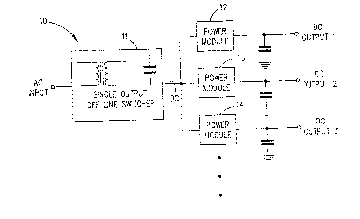
5 With initial reference to Fig. 1, a power supply
arrangement 10 includes a single output off-line
switcher 11 which converts an AC input to a single
level DC butput. The output of the off-line switcher
11 is then coupled to a number of power modules 12, 13,
10 14, etc., which are DC-to~DC converters for producing
different DC output voltages. As many converters 12-14
are employed as are necessary to produce the required
different DC outputs such as outputs 1, 2 and 3.
With additional reference to Fig. 2, prior power
15 modules, or DC-to-DC converters, have taken a number of
forms, including that of the buck converter 20 of Fig.
2a. In Fig. 2a, a conventional buck converter, or o
current step-up power converter~ 20 utilizes an FET 21
for the series switch and a diode 22 for the flywheel
20 rectifier. During normal operation of this standard
converter, the FET 21 is turned on, impressing the
input voltage, less the output voltage, across an
inductor 23. Placing this voltage across the inductor
causes the current in the inductor to increase,
25 charging an output capacitor 24 while also delivering
current to any load connected in parallel with the
capacitor.
When the FET 21 is turned off, the voltage at node 1
(the connection point for the FET 21, the diode 22 and
30 the inductor 23) falls until the diode 22 becomes
forward biased. Current then flows through the diode
22 and the inductor 23 with decreasing amplitude until
the FET 21 is again turned on and the cycle repeated.
LE9-86-011
6 ~ 3
Switching loss occurs when the FET 21 is turned on and
of~ because of the finite time required for the current
to start and stop flowing. As the FET is turned on,
current flowing through the device causes the voltage
5 on node 1 to rise, producing dissipation equal to the
instantaneous product of current and voltage at the FET
over the time interval required for turn on.
Similarly, when the FET 21 is turned off, the
simultaneous presence of voltage and current produces
10 substantial dissipation. In the past, the diode 22 has
been replaced with an additional FET (having an
orientation as shown for the FET 32 in Fig. 3a~. This
improves ëfficiency in the converter.
As earlier discussed, timing of FET turn on and turn
15 of~ becomes critical in a two FET configuration. As
also earlier discussed, it would be desirable to
increase the frequency of operation of a standard
converter such as the converter 20 in order to reduce o
the size of the reactive components in the converter. o
20 However, in increasing fre~uency, both switching loss o
and critical timing requirements become more difficult
to deal with.
Turning now to Fig. 3, a buck converter 30 configured
in accordance with certain aspects of the invention
~5 includes a series switch FET 31 and a flywheel FET 32
connected at a node, designated node 1, with one
terminal of an inductor 33. An output capacitor 34 is
provided at the output of the converter 30, and a
capacitor 36 is also provided in parallel with the
flywheel FET 32. The FET's 31 and 32 are power
MOSFET's including internal diodes. The FET 31 is a
p-channel MOSFET and the FET 32 is an n-channel MOSFET.
The source of the FET 31 is at the converter input and
the drain of the FET 31 is connected to node 1, which
LE9-86-011
~ 9
is connected to the drain of the FET 32 and one
terminal of the inductor 33. The source of the FET 32
is connected to circuit common, or ground. The gates
of the FET's are coupled to a suitable control circuit
5 as shall be described in more detail hereinafter.
,,
Each FET 31, 32 includes an internal diode, with the
internal diode of the FET 31 poled to conduct current
from node l toward the input, and the internal diode of
the FET 32 poled to conduct current from circuit common
10 to node 1. Each FET includes a parasitic capacitance,
and due to the low impedance of the voltage source
input, the capacitances of the FET's 31 and 32 are
effectively connected in parallel between node 1 and
circuit common. In many cases, a physical capacitor 36
15 is not reguired, as the FET parasitic capacitances are
of sufficient size to support the voltage at node 1
during turn-off of each of the FET's. In subsequent
illustrations of the converter of Fig. 3, the discrete o
capacitor 36 is omitted.
o
In the converter 30, the inductor 33 is selected to be
of a value to insure that the inductor current polarity
reverses during each normal cycle of operation (each
cycle of turn-on and turn-off of the series FET 31).
Insuring reversal of the inductor current requires not
~5 only the selection of the inductance value, but also
(a) the operation of the converter with a peak forward
inductor current that is not too large relative to the
size of the output voltage and (~) the provision of a
suitably long off-time for the series FET. To insure
current reversal, the output voltage must be greater
than or equal to the product of (a) the inductance of
the inductor 33 and (b) the value of the peak inductor
current (the inductor current when the series FET is
LE9-86-011
8 ~7&13~
turned off), divided by the length of the off-time of
the series FET 31.
A typical operating cycle for the converter 30 begins
with the turn-off of the FET 31, after which the node 1
5 voltage falls until it reaches æero, as the inductor 33
draws current first from the capacitor 36 and then
through the internal diode of the FET 32. The fl~wheel
FET 32 is `then turned on with zero switching loss since
the voltage across it is zero at the time of turn-on.
10 The flywheel FET 32 is not turned off until the
direction of current flow in the inductor~33 has
reversed, with current flow through the flywheel FET.
When the fly wheel FET is turned off, the capacitor 36
holds the voltage at node 1 near zero during the turn
15 off interval, after which the (now-reversed~ current
through the inductor 33 drives the node 1 voltage up to
the level of the input voltage. Note that at this time
the flywheel FET is turned off and its internal diode
is non-conductive since it is reverse biased. The ,
20 series FET 31 is then turned on with substantially no
voltage across the FET, so that there are substantially
no turn-on losses. The cycle then repeats.
It should be noted that the turn-on and turn-off of
both the series FET 31 and the flywheel FET 32 occur
25 with nearly zero volts across the FET's. Also, there
is an inherent, desirable dead time between the
turn-off of one FET and the turn-on of the other. The
turn~on of the FET 31 occurs after the inductor current
has reversed and taken node 1 to the level of V~N, and
30 the turn-on of FET 32 occurs when the inductor current
has taken node 1 low after the series FET 31 has been
turned off.
LE9-86-011
9 ~ ~ 7~ 9
The turn-on timing of the FET's is less critical
(allowing dead time) because stored charge in the FET
internal diodes has the FET on-time to recombine if
turn-on is late. That is, when each FET is turned on,
the internal diode of the other FET is reverse biased
and non-conductive so that energy is not expended in
neutralizing the stored charge associated with the
device forward voltage drop. Switch through
(simultaneous FET conduction) will not result unless
turn-on occurs prior to the normal transition dead
time. Overall conversion efficiency and ease of
control for the converter is therefore improved, and
operation at high fre~uencies is permitted.
While the presently preferred form of converter is a
buck converter, the principles of the invention are
applicable to other converter topologies such as the 2
boost converter and buck-boost converter topologies.
With reference, for example, to Fig. 4, a boost o
converter configured in accordance with the invention
includes FET's 231 and 232 interconnected at node 1 and
an inductor 233 connected between the input voltage VIN
and node 1. A capacitor 234 is connected across the
output VOUT, and a capacitor 236 is connected in
parallel with the FET 232.
A typical operating cycle begins with the turn-off of
the FET 232, after which the voltage at node 1 rises to
the level of VOUT as current in the inductor 233
charges the capacitor 236. The FET 231 is then turned
on with zero switching loss, since the voltage across
it is zero. The turn-off of the FET 231 does not occur
until the direction of current flow in inductor 233 has
reversed. After the turn-off of the FET 231, the
current in the inductor 233 draws charge from the
capacitor 236 until the voltage on node 1 is zero,
LE9-86-011
333~3
after which the cycle repeats. It should be noted that
the turn-on and turn-off of the FETIs 231 and 232 occur
at zero voltage since the capacitor 236 holds the node
1 voltage almost constant while switching occurs.
Operation and advantages are similar to those
previously described for the buck converter of Fig. 3.
With reference now to Fig. 5, the invention is embodied
in a buck-boost converter which includes FETIs 241 and
242, interconnected at node 1, to which is also
connected an inductor 243. A capacitor 244 is coupl~d
across the output VOUT~ and a capacitor 246 is coupled
across the inductor 243. A typical operating cycle of
the converter begins with the turn-off of the FET 24~.
After the turn-off of the FET 241, the voltage between
node 1 and ground falls to the level of VOUT as current
in the inductor 243 dischar~es the capacitor 246. The
FET 242 is then turned on with zero switching loss,
since the voltage across it is zero. Turn-off of the O
FET 242 does not occur until the direction of current o
20 flow in the inductor 243 has reversed. After the o
turn-off of the FET 242, the current in the inductor
243 charges the capacitor 246 until the voltage at node
1 is equal to VIN, after which the cycle repeats.
Again, it should be noted that turn-on and turn-off of
the FET's 241 and 242 occur at zero voltage since the
capacitor 246 holds the node 1 voltage almost constant
while switching occurs. The operation and advantages
of the buck-boost converter are similar to those
previously described for the other converter
topologies.
Returning to consideration of the buck converter of
Fig. 3, in order to regulate the output of the buck
converter 30, a control circuit i5 p~ovided for
,~
I
LE9-86-011
~ 3
controlling the on- and off-times of the two FET's 31
and 32.
Conventional control circuits for DC-to-DC converters
usually provide output voltage regulation in one o~
S three ways. In constant frequency pulse width
modulation, the operating frequency is held constant
while on-time of the series switch is varied to
compensate for variations in input voltage and load.
In constant freguency peak current control, the
10 operating frequency is held cons~an~ while the maximum
amplitude of the current in the series switch is varied
to compensate for variations in load. Compensation for
input voltage variations is inherent in the peak
current control. In constant on time variable
15 frequency contrGl, the series switch on-time is held
constant and off-time is varied to compensate for
variations in load and i~put voltage.
,
In the converter circuit 30, it is advantageous to
provide a control circuit which is independent of time
20 constraints such as constant frequency or constant
on-time. It has been found that the use of a control
circuit which maintains a constant peak-to-peak current
through the inductor 33 provides the requisite
regulation and is particularly suited to the converter
25 30, which has a requirement that the inductor current
reverse on each cycle of operation.
To produce output voltàge regulation and constant
peak-to-peak current, a control circuit must implement
two timing equations. The on-time of the series
30 switch, in this case the series FET 31 r is given by:
ON1 (L)(Ip_p)/(YIN ~ VOUT) (1)
.~
, ~
LE9-86-01,
12
In this expression L is the inductance value of the
inductor 33, and Ip_p is the peak to peak value of the
inductor current. VIN is the input voltage, and VOUT
is the output voltage. The on-time of the flywheel
5 device, in this instance the flywheel FET 32, is given
by:
ToN2 - (L)(Ip_p)/(VOUT) (2)
In Fig. 6 a DC to DC converter 30' (which is the same
as the converter 30 of Fig. 3 with the addition of
lO drive circuitry for the FET's) includes a drive circui~
37 for the FET 31 and a drive circuit 38 for the FET
32. These drive circuits, exemplary forms of which
shall be described in more detail hereinafter, receive
control signals from the control circuit illustrated in
15 Fig. 7 in order to control the conduc~ion times of the
FET's 31, 32. The connections of the control signals
to the drive circuits are shown by the letter o
designations A and B in the schematic of Fig. 7 and the
corresponding designations in Fig. 6.
As shown in Fig. 7, a control circuit 40 for the
converter 30' of Fig. 6 includes a capacitor 41 which
is charged and discharged to simulate the peak-to-peak
current flow through the inductor 33 in the converter.
Just as the change in current per unit time through the
inductor is proportional to the voltage across the
inductor, the change in voltage on the capacitor is
proportional to the current into the capacitor.
In the control circuit of Fig. 7, a charging circuit ~2
charges the capacitor 41 with a current during
substantially the same time interval that the series
FET 31 is turned on in the converter circuit 30'. In
the converter circuit, during this time, the voltage
, ~ .
LE9-86-011
13 ~ 7~ ~ 9
across the inductor 33 is equal to the difference
between the input voltage and the output voltage of the
converter. In the control circuit 40, the charging
circuit 42 provides a charging current to the capacitor
5 41 which is proportional to the di~ference between the
input and output voltages on the converter. Therefore,
since the tim~ intervals are substantially the same and
the charging current for the capacitor 41 is
proportional to the voltage applied to the inductor 33,
lO the voltage change on the capacitor 41 in the control
circuit is substantially proportional to the current
change in the inductor 33 in the inverter. ~
During the time interval that the series FET 31 is
non-conductive and the flywheel FET 32 is conductive,
lS the current in the inductor 33 decreases. During this
interval, the voltage across the inductor is
substantially equal to VOUT (applied in a reverse
direction). A discharge circuit 43 in the control o
circuit 40 provides a discharge current (to discharge o
20 the capacitor 41) which in steady state is proportional
to the converter output voltage during this interval.
As in the case of the charging circuit 42, since the
discharge circuit 43 discharges the capacitor 41 over
substantially the same time interval as that during
~S which the inductor 33 is connected across the output
voltage, and since the discharge current is
proportional to the converter output voltage, the
reduction in voltage on the capacitor 41 is
proportional to the reduction in current through the
30 inductor 33 in the converter.
In the control circuit 40, the voltage excursions of
the capacitor 41 are compared to a reference by a
comparator 44, the inverted and non-inverted outputs of
LE9-~6-011
14 1;~783;~
which are coupled to the drive circuits 38, 37,
respectively, in the converter 30'.
When the voltage on the capacitor 41 reaches its upper
limit, the non-inverted output (A) o the comparator ~4
5 goes low and the output of the drive circuit 37
provides a positive signal to the gate of the FET 31,
turning off the series switch, ending the current rise
in the inductor 33 for that cycle. At the same time,
the inverted output (B) o~ the comparator 44 goes high,
10 and the drive circuit 38 provides a positive signal to
the flywheel FET 32, turning on the FET. I~ practice,
the drive circuit 38 provides a delay prior to turning
on the FET 32, as shall be described in more detail
hereinafter.
15 In like fashion, when the voltage excursion of the
voltage on the capacitor 41 reaches a low limit, the
comparator 44 changes state, with the drive circuit 38
turning off the flywheel FET 32 and the drive circuit ~
37 turning on the FET 31, after a suitable delay.
In the control circuit 40~ a resistance divider made up
of resistors 46, 47 and 48 is connected across the
capacitor 41. The inverting input of the comparator 44
is connected to the junction between the resistors 46
and 47, and the non-inverting input of the comparator
44 is connected to a positive voltage reference
produced by a voltage reference circuit 49. When the
capacitor 41 is being charged by the charging circuit
42, the voltage at the inverting input of the
comparator 44 is lower than the reference voltage, and
the non-inverted output of the comparator is at a logic
high. This logic high is coupled through a resistor 51
to the base of a transistor 52, saturating the
transistor and shorting out the resistor 48 in the
LF9-86-011
15 3L;~7~3~9
resistance string. Therefore, the voltage at the
junction between the resistor 46 and the resistor 47 is
lower than the reference voltage and increasing as the
capacitor 41 charges~
.
5 The charging circuit 42 is turned on and off by
saturating and turning off a transistor 53 in the
charging circuit. During the charging interval, the
non-inverted output of the comparator 44 (at a logic
high) is coupled through a resistor 54 to the base of
lO the transistor 53, saturating the transistor and
activating the charging circuit. During the charging
interval, a transistor 56 in the discharge circuit 43
is turned off, so that the discharge circuit does not
discharge the capacitor 41. The inverted output of the
15 comparator 44 is coupled through a resistor 57 to the
base of the transistor 56, which (during the charging
interval) is turned off by the logic low on the
inverted output of the comparator.
o
The charging circuit 42 produces a current (to charge
20 the capacitor 41) which is proportional to the
difference between the input and output voltages of the
inverter circuit 30'. This current flows through a
transistor 58 from a voltage supply Vcc. The
transistor 58 is connected at the base and emitter to a
~5 diode S9 (which is preferably the base emitter junction
of an identical transistor). The transistor 58 and the
diode 59 are interconnected in the form of a "current
mirror", and the current through the transistor 58 is
identical to that flowing through the diode 59. The
30 current through the diode 59 is established by the
current through a transistor 60 and a resistor 67
connected in series with the diode 59 and the
transistor 53. This current level is in turn
established by an operational amplifier 68 in
. .
LE9-86-011 16 ~ 3~
cooperation with resis~ors 61-66 to be proportional to
the difference between the input and output voltages of
the converter 30'.
The resistors 61-66 are chosen to yield a voltage at
5 the emitter of the transistor 60 that is proportional
to the difference between the converter input and
output voltages. When the transistor 53 is turned on
by the comparator 44, the resistor 67 converts the
voltage at the emitter of the transistor 60 into a
10 current that is, as described earlier, mirrored into
the collector of the transistor 58 to charge the
capacitor 41.
In one form of charging circuit 42, the resistor 61 is
93~ ohms, the resistor 62 is 5K ohms, the resistor 63
is 8.57K ohms, the resistor 64 is lK ohms, the resistor
65 is 20K ohms, the resistor 66 is 20K ohms, and the
resistor 67 is l.llK ohms. The voltage produced at the .
emitter of the transistor 60 in this configuration is
about 0.1 times the difference between the input and
20 output voltages of the converter 30'.
The charging current supplied to the capacitor 41
through the transistor 58 causes the voltage across the
capacitor to rise until the voltage at the inverting
input of the comparator 44 exceeds the reference
25 voltage VREF. The comparator 44 then changes state,
and the transistors 52 and 53 are turned:off. The
charging current ceases, and the voltage at the
junction between the resistors 4~ and 47 rises, since
the resistor 48 is now effectively in series with the
30 resistors 46 and 47, raising the threshold voltage for
the comparator.
LE9-86-011
17 ~7~
At the same time, the transistor 56 in the discharge
circuit 43 is turned on since the inverted output of
the comparator 44 is now high, while the non-inverted
output of the comparator is low. Discharge current is
5 now permitted to flow through a transistor 69 and a
resistor 71 connected in series with the transistor 56.
When the voltage at the inverting input of the
comparator 44 falls below the reference voltage ~REF~
the comparator 44 outputs again change state, turning
lO off the transistor 56 and turning on the transistors 52
and 53 to repeat the cycle.
While the capacitor 41 is being discharged by the
discharge circuit 43, the level of the discharge
current in the transistor 69 is set by the resistor 71
15 and an error voltage applied to the base of the
transistor 69. This error voltage is proportional to
the difference between the reference voltage VREF and a
portion of the output voltage (of the inverter 30') O
determined by resistors 72 and 73 connected in the form O
20 o a resistance divider between VOUT and circuit O
common, or ground. The divided down VOuT is coupled to
the inverting input of an operational amplifier 74,
whose non-inverting input is connected to the voltage
reference VREF. A feedback network containing an
~5 impedance Z is provided for stability. The operation
o~ the control circuit 40 to establish the proper
conduction intervals for the FET 31 and the FET 32
shall now be described.
The signal A from the non-inverted output of the
30 comparator 44 is used to determine the on time of the
series pass device (series FET 31) in the converter
circuit 30'. Since the signal A is high whlle the
capacitor 41 is being charged to a set voltage by a
current proportional to VIN ~ YOUT~ the FET 31 will
, . .
LE9-86-011
18 ~ ~7~ 3
have an on time proportional to VIN - VOUT as is
required.
The signal B from the inverted output of the comparator
44 is used to determine the on time of the flywheel FET
5 32. This-signal is high, turning on the FET 32, during
the time that the capacitor 41 is being discharged by
the transistor 69 in the discharge circuit 43. The
operational amplifier 74 and surrounding circuitry
adjust the current in the transistor 69 (over a number
lO of cycles o~ operation) so that the non-inverting and
inverting inputs of the operational amplifier 74 are at
almost the same potential, in order to insure producing
the desired output voltage level at VOUT of the
converter 30'.
15 For example, if VOUT rises, the voltage at the
inverting input to the operational amplifier 74
increases and thus the output of ~he amplifier goes
down. This reduces the current through the transistor ~
69 and the resistor 71 so that the capacitor 41
20 discharges more slowly. This decreases the duty cycle
o t~e inverter 30' (by increasing the off time of the
series FET 31). This will in turn bring down the
converter output voltage to its proper level, perhaps
ater a few cycles of operation.
~5 Turning now to Fig. 8, a buck converter 30''
substantially the same as that shown in Fig. 3,
includes additional circuitry to provide current
limiting. When the converter is controlled by a
control circuit to provide constant peak-to-peak
30 current through the inductor 33, the inductor current
is substantially a triangular waveform as shown in Fig.
3d. With changes in the load on the output of the
converter, the current waveform in effect shifts upward
LE9-86-011
19
and downward to transfer more or less average current
from the input to the output, as required. The
effective output current of the converter is one~half
the sum of the maximum and minimum inductor currents.
.
5 The minimum inductor current occurs when the flywheel
FET 32 turns off, and the maximum current occurs when
the series FET 31 turns of. Since peak-to-peak
inductor current is maintained constant, the effective
output current may be held below a given value by
10 holding either the minimum or maximum current below a
defined level. The minimum current may be held below a
given level by sensing current in the flywheel FET 32
and not permitting the FET 32 to turn off until the
current has fallen to the selected minimum value. If
15 the minimum current is selected to be zero, it is
sufficient to simply sense the voltage across the
flywheel FET 32, keeping this device on until the
polarity of the voltage across it reverses. The
current limit set point will be independent of the ~
20 on-state resistance of the FET 32 since only the
polarity of the signal is sensed.
Fig. 8 illus~rates how such a current limit concept can
be implemented. During normal operation of the
converter 30'', toward the end of the conduction
25 interval for the flywheel FET 32, current reverses i~
the inductor 33 and flows in the direction of the
current arrow I2 through the FET 32. Normally, the
duration of this reverse current is established by the
converter control circuit in order to establish the
30 appropriate net forward current flow through the
inductor 33 to provide the desired regulation of the
output voltage VOUT-
. .
~9-86-011
This control of the flywheel FET 32 is represented in
Fig. 8 by the coupling of a signal from the control
circuit to the reset input of a flip-flop 36 to effect
the removal of the gate drive from the flywheel 32.
S When the flip-flop 86 is reset, its Q output goes low,
and this low is coupled to a driver 84, whose output
(the gate drive for the flywheel 32) goes low, turning
off the FET 32.
The current limit circuitry of Fig. 8 functions to
10 insure that the current in the flywheel FET 32 (and in
the inductor 33) has reversed before the control
circuit is permitted to remove the gate drive from the
FET 32. The current limit circuitry includes an FET 81
connected in parallel with the flywheel FET 32 and a
15 resistor 83 in series with the FET 81. When the
flywheel FET 32 is conductive, the FET 81 is saturated,
providing a low impedance path for the voltage across
the FET 32 to the inverting input of a comparator 82.
This permits accurate sensing of the voltage across the ~
~0 flywheel FET 32. The resistor 83 in series with the 3
FET 81 has a relatively high resistance, and
substantially the entire voltage across the FET 32 is
coupled to the comparator 82 when the FET 81 is
saturated. When the flywheel FET 32 is non-conductive,
~5 the FET 81 operates in the cut-off region, protecting
the comparator input from damage due to excessive
voltage, while allowing only a small current flow
through the sensing circuit.
Before the reversal of current in the FET 32, the
30 non-inverting input to the comparator 82 is at a lower
voltage than the inverting input, and the output of the
comparator 82 is low. This low, coupled through a
delay circuit 85 and the AND gate 87 to the reset input
of the flip-flop 86, prevents the flip-flop from being
LE9-86-011
21 3 ~7~33~9
reset and thus maintains the drive to the gate of the
fly~heel FET 32.
After the current in the flywheel FET 32 has reversed,
so that it is flowing in the direction of the current
5 arrow I2, the voltage across the flywheel FET 32
changes polarity, and the output of the comparator 82
goes high. This high output from the comparator 82 is
coupled to a delay circuit 85, the output of which goes
high after a delay which is proportional to the
10 magni~ude of the output voltage. The reason for the
delay is to allow the reverse current through the
inductor 33 to rise to a sufficient level to insure
that once the flywheel FET 32 is turned off, the node 1
voltage will rise to the level of VIN. The time
15 required for the reverse current through the inductor
33 to reach the necessary level is dependent upon the
magnitude of VOUT~ and the delay circuit 85 takes this
into account in providing the necessary delay interval o
for the reverse current to build in the inductor 33. ~,
o
After this delay interval, the output of the delay
circuit 85 goes high, and this high is one input to the
AND gate 87.
During normal operation of the converter 30'', the
output of the delay circuit 85 goes high before a logic
~5 high is coupled to the AND gate 87 from the control
circuit. Therefore, during normal operation, the
control circuit determines when the FET 32 is turned
off. However, during current limit mode, when the
control circuit is attempting to couple more energy
than is permitted from the input to the output of the
converter, the input to the AND gate 37 from the
control circuit goes high prior to the time that the
output of the delay circuit.85 goes high. Therefore,
LE9-86-011
22 ~ ~ 7~
in current limit mode, the comparator 82 and the delay
circuit 85 control the timing of the turn-off of the
~lywheel FET 32.
Whether the signal from the control circuit or the
5 output of the delay circuit 85 is the first to go to a
logic high, once ~oth of these signals are high, the
output of the AND gate 87 goes high, resetting the
flip-flop 86 and removing the drive signal from the
driver 84 from the flywheel FET 32. This turns off the
10 FET 32, permittin~ voltage to build across the flywheel
FET 32 at node l.
The current limit circuit shown in Fig. 8 is
advantageous relative to prior current limit approaches
in that a series sensing element in series with the FET
15 31 is not required. This eliminates the need for
additional high-current carrying components and permits Q
current limit sensing to be done with respect to
circuit common, or the negative rail, simplifying the ~
control circuitry. 3
Failures in buck converters that cause the series pass
device, such as the series FET 31, to appear as a
continuous low impedance can result in the input
voltage of the converter appearing at the converter
output. Since the value of this voltage may exceed the
maximum voltage rating of devices connected to the
output of the converter, a failure of this type can
destroy many devices downstream from the converter,
compounding the cost of the original failure. To
prevent this from occurring, various protection
circuits have been utilized. In one such circult, the
converter output voltage is sensed, and if it exceeds a
selected threshold, an SCR connected in parallel with
the output is gated on, impressing a low impedance
LE9-86-011
23 ~ 9
across the outpu~. A fuse is provided in series with
the series pass device, and the ensuing surge of
current when the SCR is turned on opens the fuse,
removing inpu~ power from the converter.
.
5 In Fig. 9,-a converter 30''' similar to that of Fig. 3
includes a new over-voltage protection circuit. This
circuit does not require an additional high-current
device to shunt the output as in prior systems. In
Fig. 9, a voltage divider made up of a resistor 91 and
10 a resistor 92 is coupled across the converter output.
The voltage at the junction between the resistors 91
and 92 is connected to the non-inverting input of a
comparator 94, whose inverting input is connected to a
voltage reference 93. If the output voltage of the
15 converter rises above a threshold level, the voltage at
the non-inverting input of the comparator exceeds the
reference voltage, and the output of the comparator 94
goes high. A high output from the comparator 94 sets a
latch 96, with the output of the latch high. The ~
~0 output of the latch is one input to an OR gate 97. If
the output of the latch 96 goes high, the output of the
OR gate goes high, holding on the flywheel FET 32.
During normal operation of the converter 30''', the
control signals for the FET 32 are provided from a
~5 control circuit through the OR gate 97, with the input
to the OR gate from the latch 96 merely remaining at a
logic low.
If an over-voltage condition does arise, and the FET 32
is held on by the latch 96, when the series FET 31 is
30 turned on, the resulting current surge (as current
flows through the FET's 31 and 32) opens a fuse 98
connected in series with the FET ~1 at the converter
input. Opening the fuse 98 removes the input power
from the converter.
. ~ .,
LE9-86-011
24
Turning now to Fig. 10, a buck regulator 100 including
the various aspects of the invention earlier described
includes a power portion 101, a control circuit 102,
FET drive circuits 103, 104, a current limit circuit
105, an over-voltage protection circuit 106, a node
monitoring-circuit 107, and input circuitry 108 for
controlling turn-on and turn-off of the regulator.
In the power portion 101 of the regulator, a series
switch FET 111 is coupled between the input DC voltage
VIN and a node 112 to which a flywheel FET 113 and an
inductor 114 are also coupled. The other side of the
inductor 114 is connected to the output voltage
terminal VOUT of the regulator, and the other side of
the flywheel FET 113 is connected to circuit common, or
15 ground. An input capacitor 116 is connected between
the input and ground, and an output capacitor 117 is
connected between the output and ground. These
capacitors provide filtering to reduce ripple at the
input and output. ~
A capacitor 118 is connected to the node 112 to support
the node voltage during turn off of the FET's 111 and
113. As earlier discussed, the capacitor 118 may be
omitted in many cases, if the parasitic capacitances of
the two FET's are sufficiently high. The power portion
101 of the regulator 100 operates in the same fashion
as earlier described for the circuit of Fig. 3.
In order to provide the gate signals to turn the FET's
111 and 113 on and off at suitable times, a control
circuit 102 emulates the peak-to-peak current through
the inductor 114, utilizing the voltage on a capacitor
121. The control circuit 102 operates in a similar
fashion to the control circuit shown in Fig. 7. In the
control circuit 102, certain elements of the circuit
LE9-86-011
25 ~ 7~ 9
have been shown diagrammatically, as is the case in
certain other areas of the regulator circuit of Fig.
10 .
Continuing with the description of the control circuit,
5 starting ~rom a time when the series FET 111 is
conducting, the voltage is rising on the capacitor 121
in the control circuit 102. The charging current to
increase t~e voltage on the capacitor 1~1 is provided
~rom a current source 122, which produces a current
10 proportional to the difference between the input and
output voltages of the power portion of the circuit.
During the time that the capacitor 121 is charging, a
switch 123 is closed by a logic high output 124 from an
AND gate 126.
15 During the time that the capacitor 121 is charging, a
comparator 127 compares a-fraction of the capacitor
voltage to a reference voltage. The reference voltage
is connected to the non-inverting input of the ~
comparator 127. The capacitor voltage is divided down
by a resistive divider including resistors 128, 129 and
131. As the capacitor 121 is charging, its
divided-down voltage is less than the reference voltage
connected to the comparator 127, and the non-inverted
output 132 of the comparator 127 is at a logic high.
~5 This logic high is coupled through a resistor 133 to a
transistor 134, which is turned on and shunts the
resistor 131 in the resistance divider string connected
across the capacitor 121. This results in a lower
voltage being coupled to the inverting input of the
comparator 127 during the charging cycle.
Subsequently, when the transistor 134 is turned off
during the discharge cycle, the voltage coupled from
the divider string to the inverting input o~ the
.,
9-86-011
26
comparator 127 is higher than the reference and moves
downwardly as the capacitor 121 is discharged.
The output 132 of the comparator 127 is also connected
as one input to the AND gate 126, which controls the
S switch 123. Therefore, during the time that the
capacitor 121 is charging, the AND gate 126 is enabled
to produce a logic high output 124 when a suitable high
output is obtained from the node monitoring circuit
107, as shall be described.
During the time that the series FET 111 is conducting,
a negative gate signal must be provided to the FET. In
order to accomplish this, the three inputs to an AND
gate 137 in the FET drive circuit 103 must be at a
logic high. A first input to the AND gate 137 is
supplied from the non-inverted output 132 of the
comparator 127, which durïng charging of the capacitor
121 and conduction o~ the series FET 111 is at a logic
high. A second input to the AND gate 137 is supplied
from an AND gate (having one inverting input) 138, the
output of which is normally high when the regulator is
turned on and not operating in the current limit mode.
The third input to the AND gate 137 is the output of an
OR gate 139, also in the drive circuit 103. The OR
gate 139 has one input coupled through a delay circuit
~5 141 to the non-inverted output 132 of the comparator
127. During start up, as the capacitor 121 is charged
and discharged, the delay circuit 141 will provide an
input to the OR gate 139 to begin operation of the FET
drive, even in the absence of a signal at the other
input to the OR gate 139.
The other input to the OR gate 139 is ~rom a comparator
142 in the node monitoring circuit 107. The
non~inverted output 143 of the comparator 142 is
LE9-86-011
27 ~7~
coupled to both the second input of the OR gate 139 and
the second input to the AND gate 126. Therefore,
during normal operation of the regulator 100, with the
series FET 111 conducting, and the capacitor 121 in the
control circuit charging, the output 143 of the
comparator 142 must be at a logic high. This logic
high, together with the other logic high inputs to the
AND gate 126, provides a logic high output 124 of the
AND gate 126, closing the switch 123 so that the
current source 122 can charge the capacitor 121 in the
control circuit. The non-inverted output 143 of the
comparator 142 also produces a logic high at the output
of the OR gate 139 which, together with the other two
logic high inputs to the AND gate 137, produces a logic
15 high at the output of the AND gate 137. This logic
high at the output of the AND gate 137 is coupled to an
inverting driver 144. The output of the driver 144 is
therefore a logic low, which turns on the series FET
111. . o
o
20 The function of the node monitoring circuit 107 is to
insure that the voltage at the node 112 in the power
portion of the regulator has reached a suitable level
or turn on of each of the FET's 111, 113 at the
re~uisite times. In other words, although the control
25 circuit 102 may turn off one FET and enable the turn on
of the other FET, the second FET will not be turned on
until the node monitoring circuit 107 indicates that
the voltage at the node 112 is at a suitable level.
The circuit 107 includes a resistance divider made up
of resistors 146 and 147 which divide down the node
voltage. The divided down node voltage, at the
junction 148 between the two resistors, is connected to
the non-inverting input of the comparator 142~ The
inverting input is connected to a reference voltage.
.
LE9-86-011
28 ~7~339
The comparator 142 includes a certain amount of
hysteresis, so that the outputs of the comparator
change state when the voltage at the node 112 reaches
approximately the value of the input voltage and also
when the voltage at the node 112 reaches approximately
zero. -
Prior to the time that the series FET 111 is turned on~the voltagè rises at the node 112 due to the current
reversal in the inductor 114. When this node voltage
has risen to the level of the input voltage, the
comparator 142 changes state with its non-inverted
output 143 going to a logic high, at which it remains
during conduction of the series FET 111. The outputs
of the comparator 142 do not change until the voltage
at the node 112 falls to zero, which does not occur
until after the series FET 111 has been turned off.
Therefore, during the conduction of the series FET 111,
the non-inverted output 143 of the comparator 142 ~
remains at a logic high, so that all three inputs to
20 the AND gate 137 are a logic high, producing the
appropriate gating signal to the FET 111, keeping it
turned on. The comparator 142 with hysteresis can be
replaced by two comparators if desired, one of which
compares the voltage at the node 112 to a high
25 reference and one of which compares the voltage at the
node to a low reference.
During the time that the capacitor 121 in the control
circuit 102 is charging, the discharge path for the
capacitor, through a transistor 151, is open. To
30 insure this, a switch 152 in series with the transistor
151 is opened by a logic low output from an AND gate
153. During charging of the capacitor 121, one input
to the AND gate 153, coupled from the inverted output
.
LE9-86-011 29 ~ 3
154 of the comparator 127, remains at a logic low. In
addition, during conduction by the FET 111, the node
monitoring circuit 107 produces a logic low at the
inverted output 156 of the comparator 142, which is the
5 other input to the AND gate 153. Therefore, both the
comparators 127 and 142 must change state before the
output of the AND gate 153 can go to a logic high,
closing the switch 152 to discharge the capacitor 121.
When the voltage on the capacitor 121 in the control
~0 circuit 102 reaches the level indicative of the desired
peak-to-peak current through the inductor 114, the
voltage at the inverting input of the comparator 127
reaches the level of the reference input to the
comparator r and the comparator outputs 132, 154 change
15 state.
The non-inverted output 132 of the comparator goes low,
so that the output of the AND gate 126 goes low, .
opening the switch 123 and stopping the flow of c
charging current into the capacitor 121. .The now-low
~0 output 132 from the comparator 127 also causes the
output of the AND gate 137 to go low, taking the output
of the inverting driver 144 high, turning off the
series FET 111.
The inverted output 154 of the comparator 127 goes
~5 high, providing a logic high input to the AND gate 153,
to enable the discharge circuit for the capacitor 121.
The inverted output 154 of the comparator 127 is also
coupled as one input to an AND gate 157 in the driver
circuit 104 for the flywheel FET 113. A second input
158 to the AND gate 157 is coupled from the turn on
control line 171, and is normally high when the
regulator is on. The th.ird input to the AND ~ate 157,
which is now enabled due to th~ logic high state of the
.
LE9-86-011
inverted output 154 of the comparator 127, is from the
inverted output 156 of the comparator 142. This output
will remain low until the node 112 in the power portion
of the circuit reaches approxima~ely zero, so that the
output of the AND gate 157, although enabled, will not
go to a logic high (to effect the turn on of the
fly~heel FET 113) until the node monitoring circuit 107
has detected the appro~imately zero voltage condition
on the node 112.
Since there is a short interval during which both FET's
are turned off, and also a short interval during which
both of the switches 123 and 152 in the control circuit
102 are turned off, both the inductor 114 current and
the capacitor 121 voltage will have rounded, or
flattened, peaks. As will become apparent, this occurs
m
at the turn off of each device, so that the waveforms
of the inductor 114 current and the capacitor 121
voltage are triangular, with flattened upper and lower
peaks.
20 After the series FET 111 has been turned off, and the
voltage at the node 112 fallen to zero, the
non-inverting input to the comparator 142 in the node
monitoring circuit 107 falls below the reference value,
and the comparator 142 non-inverted output 143 goes low
~5 and the inverted output 156 goes high. The logic low
on the output 143 is coupled to the AND gate 126 which
controls the switch 123 for charging the capacitor 121;
but this low input to the AND gate 126 has no effect at
this time since the other input to the AND gate is
30 already at a logic low due to the previous change in
state of the comparator 127. Likewise, coupling the
logic low which is now on the output 143 of the
comparator 142 (via the OR gate 139) to the ~ND gate
137 has no effect on the driver 144 for the FET 111,
, - ~
T,E9-86-011
31 ~ 3;~9
since the input to ~he AND gate 137 from the comparator
127 has previously gone low, already deactivating the
driver.
The now-high inverted output 156 of the comparator 142
5 does have an effect on the control circuit and the
power circuit. The output 156 is one input to the AND
gate 153 in the control circuit 102. The other input
to the AND gate 153 has previously gone high due to the
change in state of the comparator 127. Therefore, once
lO the output 156 from the comparator 142 goes high, the
output of the AND gate 153 goes high, closing the
switch 152 and permitting discharge of the capacitor
121 through the transistor 151 and a series resistor
161.
~,
15 As earlier described with regard to Fig. 7, the level
of conductance of the transistor 151 is controlled by
an amplifier 162 in a manner to maintain the output
voltage of the regulator at a desired level,
proportional to a reference voltage 163. ln order ~o
20 do this, the reference voltage is cou~led through a
resistor 164 to the non-inverting input of an amplifier
162. The regulator output voltage is coupled through a
resistor 166 to the inverting input of the amplifier
162. A feedback capacitor 167 and resistor 168 provide
25 a stable feedback loop for the amplifier 162.
The discharge circuitry for the capacitor 121 also
includes "soft start" circuitry operative when the
regulator ls turned on. During turn on of the
regulator 100, an input control line 171 goes to a
30 logic high, as shall be described in more detail
hereinafter. This logic high is connected to an
inverter 172, the output of which is coupled through a
resistor 170 to the base of a transistor 173, which
LE9-86-011
32 ~7~
shunts the non-inverting input of the amplifier 162.
This transistor 173, in cooperation-with a capacitor
174, serves to provide a "soft start" for the control
circuit. When the regulator is turned on, and the
transistor 173 turned off, the capacitor 174 is charged
by the voltage reference circuit 163 so that the full
reference value does not appear at the reference input
to the amplifier immediately upon turn on of the
regulator. This has the effect of increasing the
10 discharge interval for the capacitor 121 during start
up of the regulator. This in turn permits the
regulator to reach its normal operating level more
slowly upon turn on.
Returning to the description of the effects of the
15 logic high at the inverted output 156 of the comparator
142, not only is this logic high coupled to the AND
gate 153 in the control circuit 102 to permit discharge
of the control capacitor, but it is also coupled .
(through an OR gate 176~ to the AND gate 157 in the ~
20 driver circuit 104. This logic high input to the ~ND
gate 157 results in all three inputs to the AND gate
being high, and the now-high output or the AND gate 157
is coupled through an OR gate 177 to a driver circuit
178, whose output goes high, turning on the flywheel
FET 113. Therefore, the flywheel FET 113 is not turned
on until such time as the node 112 has reached a level
of approximately zero volts, resulting in near zero
switching loss during turn-on of the FET.
The OR gate 176 through which the logic high from the
output 156 of the comparator 142 is coupled is provided
to permit the connection of a delay circuit 179 for
start-up operation. The delay circuit 179 functions in
a manner analogous to the delay circuit 141, earlier
described.
LE9-86-011
33 ~7~33;~3
The OR gate 177, through which the turn on signal from
the comparator 142 is coupled, is provided to permit
the flywheel FET 113 to be driven on by either the
current limiting circuit 105 or the over voltage
protection circuit 106, as shall be described
hereinafter.
When the non-inverted output 132 of the comparator 127
in the control circuit 102 goes low due to the
comparator 127 changing state when the capacitor 121 is
charged to its peak value, this turns off the
transistor 134 connected in parallel with the resistor
131 in the divider resistance string connected across
the capacitor 121. As earlier described with regard to
Fig. 7, this raises the voltage of the junction between
resistors 128 and 129, so that as the capacitor 121
discharges during its discharge cycle, the voltage at
the inverting input to the comparator 127 moves
downwardly toward the value of the refPrence voltage. o
As this occurs, the voltage at the inverting input to
20 the comparator 127 reaches the value of the reference
voltage, and the comparator 127 outputs again change
state, with the non-inverted output 132 going high, and
the inverted output 154 going low.
The logic low at the output 154 of the comparator 127
25 opens the switch 152, ending discharge of the capacitor
121, and also takes the output of the AND gate 157 in
the driver circuit 104 low, effecting turn-off of the
flywheel FET 113. The logic high on the non-inverted
output 132 of the comparator 127 is coupled to the AND
gate 126 and to the AND gate 137, enabling both of
these gates.
When the voltage at the node 112 reaches approximately
the value of the input voltage to the regulator 100,
,
LE9-86-011
34 ~ 9
the comparator 142 in the node monitoring circuit
changes state. When the comparator 14~ changes state,
the non-inverted output 143 of the comparator goes
high, coupling a logic high to the already enabled AND
gates 126 and 137, so that the switch 123 is closed
beginning the charging cycle for the capacitor 121 and
the driver 144 is activated, turning on the series FET
111. The above-described cycle of operation then
repeats.
10 The over-voltage protection circuit 106 includes a
resistive divider made up of resistors 181 and 182,
with the junction between the resistors being connected
to the non-inverting input of a comparator 183. The
voltage at the non-inverting input to the comparator
15 183 r which is proportional to the regulator output
voltage VOUT, is compared to a reference value. If the
regulator output voltage exceeds the reference value,
the output of the comparator 183 goes high, and this o
logic high is coupled to a latch 185. The output of
20 the latch 185 is latched high and coupled through an OR
gate 184 and the OR gate 177 to the driver 178 for the
flywheel FET 113, turning on and holding on the FET.
Continued current conduction through the series FET
111, and through the now-conductive flywheel FET 113,
25 opens a fuse 186 connected in series with the VIN
connection to the power portion 101 of the regulator.
Although the high output of the OR gate 184 is coupled
to the inverting input of the AND gate 138 in the drive
circuit 103 for the FET lll, removing the gate drive
30 from the FET, this often will not of itself alleviate
an over-voltage condition since the FET 111 itself may
be short-circuited.
The current limit circuit 105 functions to prevent
turn-off of the flywheel FET 113 until the current
LE9-86-011
35 ~ ~ 7~ 9
through the FET has fallen below a specified value
(that is, the reverse current through the coil 114 and
the flywheel FET has exceeded a specified value~. The
time at which the current in the FET 113 passes through
5 ~ero is determined by a comparator 191. The compar~tor
191 senses~the voltage across the FET lI3, and when
this voltage goes above zero, indicative of current
reversal, the output of the comparator 191 goes high.
This output of the comparator 191 is coupled to an AND
10 gate 192, which has a second input connected to the
inp~lt to the driver 178 for the FET 113. The input to
the AND gate 192 from the driver 178 input is high when
the FET 113 is turned on. Therefore, when the voltage
at the node 112 goes above ground, and the FET 113 is
15 turned on, the output of the AND gate 192 goes high.
The output of the AND gate 192 is coupled through a
resistor 193 to a switch 194, and when the output of
the AND gate goes high, the switch 194 is closed. When
the switch 194 closes, a current source 195 is
20 permitted to charge a capacitor 196. The current
provided by the current source 195 is proportional to
the level of the output voltage VOUT.
The level of the voltage on the capacitor 196 is
coupled to the inverting input of a comparator 197,
~5 whose non-inverting input is connected to a voltage
reference. When the voltage on the capacitor 196
e~ceeds the reference voltage, the output of the
comparator 197 goes to a logic low. This low output of
the comparator 197 is one input to an AND gate 198,
30 whose other input is connected to the input of the FET
driver 178. Therefore, when the FET 113 is turned on,
and after the capacitor 196 in the current limit
circuit 105 has charged sufficiently, the output or the
AND gate 198 then goes low, and the output of the OR
35 gate 184 goes low. This takes one of the inputs ~o the
LE9-86-011 36 ~ ~ 78~9
OR gate 177 low, and when its other input (from the
control circuit 102) has gone low, this will deactivate
the driver 178 and turn off the FET 113.
The delay in turn off of the flywheel FET 113 caused by
5 current in the current source 195 charging the
capacitor 196 provides a time interval during which
current increases in the flywheel FET o Since the
current charging the capacitor 196 in the current limit
circuit 105 is proportional to VOUT, as is the reverse
10 current through the inductor 114, the current flowing
into the flywheel FET 113 at the time of turn off will
have a specified value during current limit operation
which is independent of the actual value of VOUT. This
insures that there will be sufficient energy in the
15 inductor when the flywheel FET 113 is turned off to
subsequently bring the voltage at the node 112 up to
the level of VIN to permit lossless turn-on of the
series FET 111. ~
o
In cases where the circuit is not operating in current
20 limit mode, the input to the OR gate 177 from the OR
gate 184 can go low upon the determination by the
current limit circuit 105 that there is suitable
reverse current flowing throu~h the FET 113, without
this turning off the FET 113. This is because the
25 other input to the OR gate 177, produced from the
control circuit 102, can remain high, which produces a
high output of the OR gate 177 so that the driver 178
keeps the FET 113 turned on.
When in current limit mode, holding on the flywheel FET
113, the ~urn on of the series FET 111 is prevented.
To do this, the output of the OR gate 184, which is at
a logic high during current limit mode, is connected to
the inverting input of the AND~gate 138 in the driver
LE9-86-011
37 ~;~78;~3~
circuit 103. This causes the output of the AND gate
13~ to be low, which produces a low at one of the
inputs to the AND gate 137 controlling the driver 144
for the FET 111. Therefore, a drive signal for the
S series FET 111 is not provided during current limit
mode. Norj as earlier mentioned, is such a drive
signal provided in the over voltage situation where the
other input to the OR gate 184 is high.
In order to reset the current limit circuit 105, each
time the series FET 111 is turned on, meaning that a
logic high signal has appeared at the output o~ the AND
gate 137 in the FET driver circuit 103, this logic high
is coupled through a resistor 201 to the base of a
transistor 199 connected in parallel with the capacitor
196 in the current limit circuit, turning on the
transistor 199. Turning on the transistor 199
discharges the capacitor 196.
In the input circuitry 108, the output 171 of an AND
gate 202 serves as a turn on control line for the
regulator 100. The line 171 is normally high when the
regulator 100 is turned on. One input to the AND gate
202 is an on/off line, which is high when, for example,
a power-on switch is activated. Two other inputs to
the AND gate 202 must be high in order to activate the
regulator 100. One of these insures that the input
voltage is above a desired threshold, and the other
insures that the temperature of the FET's is below a
critical level.
In the section 108 of the regulator 100, the input
voltage VIN to the regulator is divided down by a
resistance divider made up of a resistor 203 and a
resistor 204. The divided down VIN is compared to a
reference voltage by a comparator 206, which contains
LE9-86-011
38 ~ ~'7~
an amount of hysteresis, or which may be used in
conjunction with a latch, with the output of the
comparator 206 being normally high, but going low if
the input voltage to the regulator is too low~ The
out~ut of the comparator 206 is one input to the AND
gate 202. -
A thermal shutdown circuit, which produces the thirdinput to the AND gate 202, includes a comparator 207,
whose inverting input is connected to a resistance
divider made up of resistors 208 and 209, coupled
between a reference voltage and ground. The same
reference voltage is also coupled through a resistor
211 and a diode 212 to ground. The diode 212 is
physically located near the power FET's 111 and 113,
15 and the diode characteristic is such that the voltage m
across the diode decreases as the temperature
increases. If the temperature of the diode 212
increases sufficiently, and its voltage decreases o
sufficiently, the voltage across the diode, which is
20 connected to the non-inverting input of the comparator
207, falls below the level of the reference voltage
coupled to the inverting input of the comparator 207.
If this occurs, the output of the comparator 207, which
is normally high, goes low, taking the control line 171
25 low.
. .