Note : Les descriptions sont présentées dans la langue officielle dans laquelle elles ont été soumises.
33
BACKGROUND OF THE INVENTION
Field of the Invention
The present invention relates to a device for
reproducing a synchronizing clock signal from a series signal
which has been modulated by coded modulation in synchronism
with a clock signal of a prescribed period, the reproduced
synchronizing clock signal being synchronous with the clock
signal.
Description of the Prior Art
For transmitting digital data over a telephone line
or a data line or recording digital data on a recording medium
such as a magnetic disc, an optical disc, or the like,
a practice widely used has been to modulate the digital data
into a series signal encoded in synchronism with a clock
signal of a prescribed period.
Examples of such encoding processes include NRZ
(Nonreturn-to-Zero), N~ZI (Nonreturn-to-Zero Inverted), PE
(Phase Encoding), FM (Frequency Modulation), and MFM (Modified
Frequency Modulation).
The signal encoded by these encoding methods is
a code modulated by clock pulses (hereinafter referred to as
a "bit clock") having a period equal to a data bit interval TB
which is a time interval representative of one-bit data on
a time-series basis. The interval of polarity inversion, the
interval between positive-going edges, and the interval
between negative-going edges of the encoded signal are each
equal to a multiple of TB or TB/2.
- 2 - h
1'" j~
~L27~ 3
For demodulating the encoded series signal to obtain
the origina~ data, i~ is o~ten necessary to reproduce the bit
clock used in the encoding process from the modulated signal.
It is customary to reproduce clock pulses having the same
period as that of the bit clock or a period equal to the
period of the bit clock as divided by an integer, using
a positive-going edge or a negative-going edge of a signal
pulse, and to shift the phase of the reproduced clock pulses
or frequency-divide the reproduced clock pulses to produce
a demodulating synchronizing clock.
The synchronizing clock may typically be reproduced
by one of the following two methods:
(1) A counter supplied as a clock input with
a frequency that is a multiple (normally by 16 or 64) of that
of the synchronizing clock is operated, and cleared by
a positive-going edge or a negative-going edge of a signal
pulse. The frequency-divided output of the counter is thus
synchronized with the pulse signal edge, thereby reproducing
the synchronizing clock.
(2) A bit clock insertion zone called
a synchronlzing field is provided in the initial portion of
the modulated signal. A phase-locked loop circuit
(hereinafter referred to as a "PLL circuit") is operated
within the bit clock insertion zone to reproduce the
synchronizing clock.
The circuit for carrying out the method (1) is very
simple, but has problems in that jitter corresponding to one
~~7~ 3
period of the clock input applied to the counter cannot be
avoided, and the circuit tends to respond when the positive-
going edge or negative-going edge of the modulated signal
pulse is disturbed by noise.
The method t2) employs a feedback loop and has much
better characteristics than those of the method (l) with
respect to jitter and noise. However, this method requires
a complex circuit since the synchronizing field is provided.
Because synchronization is achieved basically only in the
synchronizing field, a long-term nonsynchronous condition is
apt to occur when a long continuous signal of more than
several thousand bits is demodulated. This nonsynchronous
condition has to be corrected by a suitable method.
SUMMARY OF THE INVENTION
In view of the aforesaid conventional problems, it
is an object of the present invention to provide a device for
generating a synchronizing clock without causing a long-term
nonsynchronous condition even when demodulating a long
continuous signal of more than several thousand bits, the
device being resistant to jitter and noise.
Where a synchronizing clock is reproduced by using
a conventional PLL circuit, it is necessary to provide
a synchronizing field because a reference input signal of
a constant ~requency has to be applied. In view of this,
an ordinary PLL circuit is combined with a signal delay
circuit for delaying a reference input signal by a prescribed
time and issuing a reference signal, and a shift register
~2~
receptive of the reference input signa~ and a clock signal
which is an oscillation signa~ from a voltage-controlled
oscillator or a signal produced by frequency-dividing the
oscillation signal by an integer, for issuing a comparison
signal in synchronism with the clock signal. The comparison
signal and the reference signal are compared in phase~ With
this arrangement, no synchronizing field is necessary, and
long-term nonsynchronous condition is eliminated.
Even if the reference input signal is not a pulse
signal of a fixed frequency, a synchronizing clock signal can
be reproduced in synchronism with the reference input si~nal,
as is the case with a conventional PLL circuit supplied with
a signal of a constant frequency, insofar as the reference
input signal is a pulse signal with its polarity inverted at
the time of a multiple of a prescribed natural period.
The above and other objects, features and advantages
of the present invention will become more apparent from the
following description when taken in conjunction with the
accompanying drawings in which preferred embodiments of the
present invention are shown by way of illustrative example.
BRIEF DESCRIPTION OF THE DRAWINGS
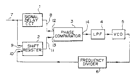
Figure 1 is a block diagram of a device according to
the present invention;
Figure 2 is a block diagram of a phase comparator in
the device of the present invention; and
Figure 3 is a timing chart of operation oE the
device shown in Figure 1.
7~83~
DESCRIPTION OF THE PREFERRED EMBODIMENTS
In Figure 1, the arrowed lines represent signal
lines, and the arrows indicate the directions in which signals
are transmitted. A device or synchronizing clock signal
generator according to the present invention includes a phase
comparator 3, a low-pass filter 4, a voltage-controlled
oscillator 5, and a frequency divider 6 (which may be omitted)
which are components of a conventional PLL circuit. The
synchroniziny clock signal generator also includes a signal
delay circuit 1 for delaying a reference input signal from
a signal line 7 by a given period of time and for issuing the
delayed reference signal to a signal line 8, and a shift
register 2 for delaying the reference input signal applied to
an input terminal 9 in synchronism with a clock signal applied
to a clock input terminal 10 and for issuing a comparison
signal to a signal line 11. The signal delay circuit 1 and
the shift register 2 are respectively connected to input
terminals 12, 13 of the phase comparator 3. The phase
comparator 3, the low-pass filter 4, the voltage-controlled
oscillator 5, the frequency divider 6, the signal delay
circuit 1, and the shift register 2 jointly constitute
a feedback loop which is stabilized when the reference signal
applied to the input terminal 12 and the comparison signal
applied to the input terminal 13 are in phase with each other.
Figure 2 shows, by way oE example, a circuit
arrangement that can be used as the phase comparator 3. The
two input pulse signals, i.e., the reference signal and the
~8~ 33
comparison signal, are applied to the input terminals 12, 13
and compared with each other as to phase. ~ signal
representative of the phase difference between the two input
pulse signals is sent to an output terminal 14. The phase
comparator 3 of the present invention is not limited to the
illustrated structure, but should preferably be of the digital
type and of the type in which synchronization is stabilized if
it is used in a conventional PLL circuit when the phase
difference between the two input signals is zero.
Figure 3 is an operation timing chart of the
synchronizing clock signal generator. In Figure 1, the
oscillation frequency of the voltage-controlled oscillator 5
and the frequency~dividing ratio of the frequency divider 6
are selected such that the natural period Ts of a reference
input signal 20 and the period T of a clock signal 22 after
synchronization are equalized. The shift register 2 has
a shift bit number n of 1 ~equivalent to one D-type flip-
flop), and is of the type which can be operated by a positive-
going edge of a signal applied to the clock input terminal 10.
The phase comparator 3 has the circuit arrangement shown in
~igure 2.
A reference siynal 21 and a comparison signal 23
which are applied to the input terminals 12, 13 of the phase
comparator 3 are compared in phase by the phase comparator 3.
During a phase layging zone 25, the phase of the comparison
signal 23 lags behind the phase of the reference signal 21.
Therefore, a positive pulse is issued as an output signal 24
~7~3~
from the phase comparator 3 to shift the oscillation frequency
o~ the voltage-controlled oscillator 5 through the low-pass
filter 4 toward a higher frequency, so that the period of the
clock signal 22 becomes progressively shorter. In a phase
leading zone 26, the phase of the comparison signal 23 leads
the phase of the reference signal 21. A negative pulse is
issued as an output signal 24 from the phase comparator 3 to
progressively increase the period of the clock signal 22. In
a synchronizing zone 27, the phase difference between the
reference signal 21 and the comparison signal 23 is zero, and
the waveforms of these two signals 21, 23 coincide with each
other. The clock signal 22 is synchronized with the reference
input signal 20, and serves as a synchronizing clock signal.
Assuming that the signal delay circuit 1 has a delay time T,
and the response delay time of the comparison signal 23 with
respect to a positive-going edge of the clock signal 22 is TA,
the time difference Tl between a positive-going edge of the
clock signal 22 and a positive-going edge of the reference
input signal 20 is of a constant value expressed by:
Tl = T - TA.
Now, a natural period zone 27' equal to the natural
period Ts of the reference input signal 20 in the
synchronizing zone 27 will be considered. It is assumed that
the time differences between the opposite ends of the natural
period zone 27' and the positive-going edge of the clock
signal 22 are indicated by Tl, T2, respectively. No phase
difference is produced between positive-going edges of the
1333
reference signal 21 and the comparison signal 23 if ~he
positive-going edge o~ the clock signal 22 lies in the natural
period zone 27'. The times Tl, T2 therefore indicate time
margins of positive- and negative-going edges of the reference
input signal 20 with respect to jitter. Thus, when
Tl = T2,
the margin of the reference input signal 20 with respect to
jitter is maximum. Based on this, a delay time Topt in which
the margin of the reference input signal 20 with respect to
jitter is maximum is determined as follows:
Since Tl + T2 = TS = T, Tl = T - TA,
Topt = Ts/2 + TA = T/2 + TA (1)
By applying the equation (1) to the case where the
shift bit number of the shift register is n and Ts = i x T
(i = 1, 2, 3, .. ),
Topt = (n - ~) T ~ TA (2)
In view of the fact that Tl > 0, T2 > 0, the
comparison signal is delayed by the time T each time the shift
bit number of the shift register is incremented by 1, and this
delay must be corrected by the delay time T, T must be within
the range of:
(n - l)T ~ TA < T < nT ~ TA (3)
The signal delay circuit 1 thus serves to correct the time
delay of the comparison signal caused by the shift register 2
and give an appropriate margin to the reference input signal
with respect to jitter.
The value of T which can practically be used is in
the range of:
78~33
(n - 0.75)T + TA < T < (n - 0.25)T ~ TA (4)
The margln of the reference input signal with
respect to jitter is maximum when T is maximum, i.e., T = Ts.
The circuit arrangement should preferably be designed to meet
this condition~ However, the present invention is not limited
to this, and the design parameters may be determined in view
of the degree of jitter of the reference input signal and the
required margin.
In the illustrated embodiment, the PLL circuit is of
a basic arrangement. However, almost any PLL circuit form may
be employed in the present invention.
The synchronizing clock signal generator according
to the present invention includes the signal delay circuit and
the shift register added to the PLL circuit. Therefore, even
if the reference input signal is not a pulse signal of a fixed
frequency, a synchronizing clock signal can be reproduced,
insofar as the reference input signal is a pulse signal with
its polarity inverted at the time of a multiple of
a prescribed natural period. The synchronizing clock signal
generator is resistant to jitter and noise. No long-term
nonsynchronous condition is developed even when demodulating
a long continuous signal of more than several thousand bits.
Although a certain preferred embodiment has been
shown and described, it should be understood that many changes
and modifications may be made therein without departing from
the scope of the appended claims.
-- 10 --