Note : Les descriptions sont présentées dans la langue officielle dans laquelle elles ont été soumises.
1;~7~
-- 1 --
This invention relates ko an electronie circuit
element, and more partieularly to an electronic circ~lit element
which is adapted to be fixedly mounted on a printed eircuit board
by soldering whi:Le being stahly provisionally fi~ecl on the boarcl
by means of an adhesive.
Conventionally, mounting of a pluralit~ of electronic
eircuit element.s on a single printed eireuit board is typically
carried out in such a manner that a prede~ermined number of
electronic circuit elements are provisionally helcl at
predetermlned positions on the printed eircuit board and then
practicall~ secured to the printed circuit by soldering.
Such an e:Leetron:ic eircuit élement is generally
classified into t~ro types or a surface-mounted-type electronic
circuit element which :is adapted to be fixecl on a conductive
pattern formed on a printed circuit board and a lead-type
electronic cireuit element which i5 adapted to be vertically
mounted with respect to a printed eircuit board by securely
inserting lead wires of the element via through-holes of ~he
printed circuit hoard and soldering ~he lead wires to the board.
The surfac~e-moul-ted-t~pe electronic eircuit element
includes a ehip-type electronic cireuit element sueh as a chip
eapacitor or -the like ancl a speeial-~ype eleetronic eircuit
element such as an IC or the like. Provisional or temporary
fixing of the surface-mounted-type electronic circuit element
on a printed circuit board which is carried out prior to
soldering operat:ion.is generally performeclb~ previou~].y applying
an adhesive to a circuit element mounting portion of the printed
circuit hoarcl by screen printing or the like ancl then placing the
circuit element on the printed eireuit board hy means of a
suction head of an automatie mounting apparatus to provis:ional:l~
fix the element on the printed eircuit board -through the
adhesive. Previ.ous applieation of the aclhesi.ve to the printed
eireuit board renders direct staekillg o-f the printed eircuit
boards impossihle, resulting in hanclling of the prin~ecl c:ircuit
boards being highl~ troublesome. In view of such a problem, it
~y~
2~7887~
~ .
is proposed that the provisi.onal fixing is carried out by
previously preparing an electronic cixcuit element series which
comprises a carrier tape and a plura].ity of electronic Gircuit
elements helcl on the carrier tape through a thermosetting
adhesive applied onto a flat surfaee o~ thè earrier tape, then
extracting the circuit elements one by one from the carr:ler tape
by means of a suction heacl of an automatic mountin~ apparatus and
placing the circuit elements on a printed circuit board `oy the
suction head to provisionally fix them on the printed circuit
board through ~he thermoset-ting adhesives ~7hi.ch may aclhere to the
sides of the electronic circuit elements when the electronic
circuit elements are removed from the tape. An example of an
electronie circuit element series of this kind is found, for
example, in Japanese Utility Model Registration No. 1405587
lJaPanese Utility Model Publieation No. 1143~/1981) to TDK
Corporation.
Unfortunately, the proposed technigues fail to
facilitate operation of releasing or extracting the electronic
circuit elernents from the carrier tape by the su~tion head
because the adhesive firmly holds khe circuit elements on the
carrier tape to a degree sufficient to prevent the smooth
peeling-off. Even ~7hen the electronic circuit element is
released from the t~pe, it pulls the carrier tape through the
adhesive during the peelin~-off operation. This results in the
carrier tape acting on electronic circuit elements adjacent to
the released one when it elastically returns to the original
position, to thereby cause them to he separated from the carrier
tape. Another disadvantage of the prior art is that the adheslve
remains on the carrier tape to fail in sticking to the circuit
element when the element is peeled off from the carrier.tape.
~ lounting of a lead-type electronic cireuit element on
a printed ci.rcuit board is generally carried out by clinching
operation wherein lead wires of the ~ircuit el.ement inserted via
througll-holes of the printed circuit board are each
perpendieularly bent at a t:lp end -thereof p:rojectecl outwardly
from the boarcl, so that the circuit element may be provisionally
. .,
12~887~
-- 3 --
fixed on the printecl circuit board by cooperation between -the
bent lead wires and a kin~ formecl along an axis of ~ach of the
lead wires by bending. Then, the fixed lead-type electronic
circuit element is practically secured to the printed circuit
board by soldering the bent ends o~ the lead wires onto a rear
surface of the printed circuit boarcl.
Unfortunately, the above-described fixing proeedure
causes the lead type electronic circuit element to fall down
duriny the provisional fixiny operation or transportation to a
soldering station. This not only leads to a failure in the
mounting but callses the perpendicularly bent tip end portions
of the lead wires of the falling-down circuit element to hinder
mounting of circuit elements adjacent thereto. Thus, the
procedure fails in high density mountiny of chip-type circuit
elements on a printed circuit board.
The present invention has been macle in view of the
foregoing disadvantages of the prior art.
Accordingly, it is an object of the present inventlon
to provide an electronic circuit element which is capable o~
positively and stably accomplishing its provisional fixiny on a
printed circuit board substantially free of any trouble.
It is another ob~eet of the present invention to
provide an electronic circuit element which has an adhesive
capable of exhibiting adhesion sufficient to positively carry out
provisional fixing one of the electronie circuit element on a
printed eircuit board therethrough.
It is a further objeet of the present invention to
provide a surface-mounted-type electronic circuit element which
has an adhesive capable of exhibiting adhesion suffieient to
positively attain provisional fixing of the electronie circuit
element on a printed cireuit board.
It is still another ob-lect of the present :invention to
provide a surfaee-mounted-type electronic circuit element which
is capab:le of beiny readily taken out or extracted for the
~ ~2'-~3876
mounting on a prlnted eircuit board, irrespective of a manner of
holding of the eircuit element prior to the extraction.
I-t is yet another object of the present invention to
provide a surface-mounted-type electronic circui.t element which
is eapable of facilitating operation of provisionally fixing the
eireuit element on a printed cir~uit hoard.
It is still a further objeet of the present invention
to provide a lead-type e:leetronic circult element whieh is
eapable of aeeomplishing its provisional fixing on a printed
cireuit board substantially free of any trouble and without any
elinehing treatment of lead wires.
It is yet a further ob~ect of the present inven~ion to
provide a lead-type eleetronic circuit element ~hich is capable
o~ significantly deereasing an area and/or a spaee recluired to
solder lead wires of the electronic circuit element to a printed
cireuit board to aecomplish high density mounting.
It i~ an even further object of the present invention
~o provide a lead-type eleetronic eireuit element whieh is
capable of faeilitating operation of provisionally fixing the
eireuit element on a printed ~ireuit board.
In aeeordance with the present invention, an electronic
circuit element is provided. The element ineludes an element
body. The element body is provided with adhesive means on a
surface thereof opposite to a printed circuit board on which the
eleetronic eircuit element is to be mounted. The adhesive means
is formed of a material whieh exhibits adhesion upon being
heated.
The adhes.tve means ma~ be formed of a polymerle
material seleeted from the group eonsisting of silicone and
aerylie and exhibit:ing adhesion when it is heated to about 80 C.
The electronic circuit element of the present invention
may be embodied :Ln the form of both a surfaee-mounted-type
electronic circui.t element which includes at least one external
terminal arranged on the element body and a lead-type one wh:leh
includes a pad memher of a predetermined thickness moun-ted on
~7~3876
the surface of the element body opposite to the printed circuit
board.
In the surface-mountecl-type electronic circui~element,
the adhes.ive means may take the form of a film layer. The
external term:inal may have a solder layer which is ~ormed of a
polymeric material ar.ranged thereon.
~ n the lead-type electronic circuit element, the pacl
member may be formed of a polymeric foam material, which is
expanded to the predetermined thickness by heating.
These ancl other objects and many of attendant
advantayes of the present invention w:l:ll he readily appreciated
as the same becomes hetter understood by referen~e to the
following detailed descrip-tion when conside:red in connection with
the accompanying drawings; wherein:
Fig. 1 is a perspective view illustrating a surface--
mounted-type electronic circuit element which is one embodiment
of an electronic circuit element according to the present
invention;
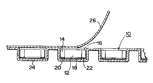
Fig. ~ is a side elevation view in section showing an
embossed tape, in recesses of which the circuit elements shown
in E'ig. 1 are received;
Fig. 3 is a schematic view showiny a manner of mounting
of the circuit element of Fig. 1;
Fig. 4 is a front elevation view illustrating a lead-
type electronic circuit element which is another embodiment of
an electronic circuit element according to the present invention,
the electronic circui-t element being provided with a pad member
of a predetermined thickness ancl fixedly mounted on a printed
circuit board;
Fig. 5 :is a schematic view showing a pad member formed
of a polymeric foam material;
Fi.g. 6 is a schematic v:iew showing -the pad member o~
Fig. S, whi.ch is expanded to a predetermined thickness by
heating;
'`'~`~ lz7~a~6
-- 6 -
Fig. 7 is a schematic view showing leacl-type electronic
circuit elements each having the p~d member of Fig. 5 mounted
thereon which are held in a row on a tape; and
Figs. ~ to 11 are schematic views showin~ a manner of
mounting of the lead-type electronic circuit element of FicJ. 7
on a printed circuit board.
Now, an electronic circuit element according to the
present invention will be described hereinafter with reference
to the accompanyillg drawings.
First, the present invention will be described with
reference to a surface-mounted-type electronic circuit element
which is one embodlment of the present invention and illustratecl
in Figs. 1 to 3.
A surface-moullted-type electronic circuiteLement shown
in Figs. l to 3 takes the iorm of a chip-capacitor and is
generally designated by reference numeral 10. The chip capacitor
10, as shown in Fig. l, generally includes an element body 12
formed into a substantiall~ rectangular shape and at least one
external terminal. In the illustrated embodiment, it includes
two external terminals 14 and 16 integrally mounted on both sides
of the element body 12. The element body 12 is provided with
adhesive means 18 on a surface thereof opposite to a printed
circuit hoard on which the chip capacitor is to be mounted.
In the illustrated embodiment, the adhesive means 18 is in the
form of a film layer which is formed of a polymeric material
deposited on the surface of the element body 12. However, the
adhesive means 18 is not limited to the form of a film layer.
Also, in the illustrated embodiment, the element body 12 is
adapted to he placed on a printed circuit board with its bottom
surface facing to the printed circult board, and the film layer
18 is deposited on a portion of the bottom surface of the element
body :L8 except the external terminals 14 and L6. The aclhesive
means or polymeric film layer 18 may be formed oE a polymeric
material which exhibits adhesion upon being heated. For example,
it may be formed of a polymeric materiaL selectecl
1~278~376
from ~he group ~onsisting of silicone and acrylic an~ exhibi~.ing
aclhesion when i-t is heated to a temperature as low as about
80 C. The adhesive means 18 is ln the iorm o~ a film layer
having a smooth or lubricious surface at a normal temperature.
The external terminals 14 and 16 have solder layers 20 and 22
prev:iously deposited thereon, respectiveL~, which are formed of
a solder material which effects solderi.ng at a temperature as low
as about 100C. and remelted at a temperature of about 130 C.
The chip capacitor 10 constructed as descrihed above,
as shown in :E'ig. 2, is received in each o:E recesses of an
embo.ssed tape 2~ in a manner such that the bottom surface of the
chip capacitor on which the po].ymeric film layer 18 is deposited
faces downwardly. After a predetermined number of the chip
capacitors 10 are received in the recesses of the embossed tape
24, the embossed tape is covered with a top tape 26 for safe
storage and -transportation of the chip capacitors. Thus, a
series of the chip capacitors which are successively fed to a
suction head of an automatic mounting apparatus descr:Lbed
hereinafter is formed.
When a chip capacitor 10 received in each of the
recesses of the tape 24 is to be mounted on a printed circuit
board, the cover tape 26 is peeled o~f from the embossed tape 24
to expose the chip capacitor 10. Subsequently, a suction head
H is actuated to hold by suction and extract the chip capacitor
10 from the tape 24. Then, a polymeric film layer 18 adhering
to an element body 12 of the chip capacitor lO having been held
by the suction heacl H is subjected to a heating treatment using
hot air e~ected from an injection nozz:Le N as shown in Fig. 3
before the suction head H is lowered to cause the chip capacitor
10 to he placed on a printed circuit boarcl P. The heating
~reatment may be carried out using, as the hot air, air heated
to a temperature of about 80C. resulti.ng in the polymeric film
layer 18 exhibiting adhesion. Then, the suction head H having
the capacitor 10 held thereon by suction is moved downwardL~ to
cause the element body 12 to be placecl on the printed circuit
~2~8~6
-- 8
board P by the heated adhesive means 1~, resulting in the chip
capacitor 10 ~eing provisionally fixed on the printed circult
board P. At this time, the solder-deposited sux~aces of the
external terminals 1~ and 16 are brought into contact with a
conductive pattern (not shown) previously formed on the prinked
circu:it board P. The above-described procedure is substantially
repeated to provisionally fix a predetermined number of circuit
elements on the printed circuit board P to form a desirecl
electronic circuit. The.rea~ter, the printed circuit board P
having the electronic circuit elements provisiona:Lly fixed
thereon is passed through a heating oven having been maintained
at a temperature of about 100 C. to melt the solder layers 20 and
22 of the electronic circuit elements, resulting in the circuit
e:Lements being practically fixed on the printed circuit board P
b~ the melted solders 20 and 22.
The above description has been made in connection with
surface mounting of the chip capacitor. However, it is a matter
of course that it is applicable to an electronic circuit element
having lead wire~ as external terminals such as IC or the like.
Alsor the chip capacitor of the illustrated embodiment is so
constructed that it may be securely mounted on the printed
circuit board by ~irmly fixing the external terminals on the
printed circuit board by means of the solder layers 20 and 22
deposited thereon. Alternativel~, the fixlng may be carried out
by means of a hot-melt type solder, a cream solder or the like
which is previously applied onto a surface of the prin-teclcircuit
board P by printing.
As can be seen from the foregoing, the surface-mounted-
type electronic circuit element which is one embodimnent oE the
present invention can be readi;ly f:Lxed on a printed circuit board
at a relatively low temperature and for a short period of time,
so that it may allow the mounting to be accolnplished at a low
cost even when it lacks heat resistance.
.
..
X~788~7Ç;
Also, in the surface-mounted--type eleckronic circuit
element of the .illustrated embodiment, the adhesive means which
does not exhibit any adhesion at a normal temperat~lre and
exhibits adhesion only when it is hea-tecl is provicled for use
temporary fixing of the electronic circuit element on a printed
circuit board. Such construction not only permits a suction head
of an automatic mounting apparatus to readily extract the
electronic circuit element from an embossed tape wlthout any
trouble because the adhesive means does not exhibit any adhesion
at a normal temperature but allows the element body to be
positively provisionally fixed on a printed circuit board by the
adhesive means 1~ which has exhibited adhesion by heating.
Now, a lead-t~ype electronic circuit element which is
another ernbodiment of an electronic circuit element according to
the present invention will be described hereinafter with
reference to Figs. ~ to ll.
A lead-type electronic circuit element of the
illustrated embodiment which is generally designated by reference
numeral 11 in the drawings, as shown in Fig. 4, generally
includes an element body 13 and lead wires 15 and 17 projecting
downwardly from a bottom surface of the element body 13. The
elemant body 13 is provided with a pad member 21 having a
predetermined thickness. The pad member 21 is stuck through an
adhesive 19 on a su.rface of the element body 13 which is opposed
to a printed circuit board P when the lead wires 15 and 27 are
inserted via through-holes ~not shown), which is prevlously
formed in the printed circuit boarcl P, to vertically mount the
circuit element 11 on the printed circuit board P. In the
illustrated emboclimerlt, the pacl member mounting surface of the
element body 13 is its bottom surface. Also, the pad rnember 21
has adhesive means 23 previously applied to a surface thereof
which is opposed to the printed circuit board P when the lead
wires 15 and 17 are inserted through the through-holes of the
board P. The adhesive means 23 may take the form of a ~ilm layer
which is formed of a polymeric material. However, it :is not
limited to such a film layer form. The pad member 21 may be
8~
- 10 -
formed into a size lonclitudinally and laterally smal].er tthan the
element hody 13. A:lternati~ely it may be formecl into
substantially the same size as the element body 13. Also the
pad memher 21 is fcormed so as to have a predetermined thickness
or a thickness ~hich permits the adhesive means ~3 to be
pressedl~l brought. ints contact with a surface of the p:rilltecl
circuit board P ~1hen the lead ~ires 15 and 17 are inserted
throuqh the throuyh-holes of the printed circuit bnartl ~' to
vertically mount the electronic circuit element 11 on the printed
cireuit board hy a desi.rell height.
The adhesives 19 and 23 or at least the adhPsi-Je 23
wh:ich :is app.Liecl to the surface of the pad member 21 opposite to
the printed circuit board is preferably ~ormecl of a polymeric
material wllictl :is capabl.e of exh:ibitinsl adllesion when :it :is
heated to a temperature oE about ~0C. such as, for example,
silicone, acrylic or ~he like. The so-formed aclhesive 23
efiectively prevents dust and/or dust from adhering thereto
before mounting of the ele~tron:ic circuit element onto -the
printed circuik board or during storage of the circuit element.
In the lead-t~pe electronic circuit elemen~ 11.
constructed as described above, ~7hen the adhesive 23 is softened
by hea~ing ancl then the lead wires lS and 27 are inserted throucJII
-the through-holes of the printed circuit board P, the element
body 13 is stab:Ly provisionally fixed through the pad member 21
on the printed circuit board P by means of the softened adhesive
23. Thus the lead-type e].ectron:lc circuit element oE the
illustrated embodiment eliminates a necessity of downwardly
projectincl tip encls of the leacl wires 1.5 and 2-/ from the p:r:in~ed
circuit board P for clinching operation as in the pr:ior art.
Each of the ].ead wires 15 and ll :ls pre~erab:Ly proiected at t;he
tip end from the printed circuit board P by a length suffic:Lent
to ensure slnootl,solde:rinc~operatiorlclesc.ri.becl hereinafter. When
it is desired to lncrease a length of the lead wires 15 and 27
as recluired in the case that ~he lecad wires 15 ancl 27 a:re hel.cl
on a carrier tape, :Eor example for storage of the lead-type
electronic circu:it elemellt, the excess of each o:E the ].eacl wireC;
,
.~ ~ ~
~L27~3~376
ma~ be removed by cutting after the lead wires are inserted
through the prin~ed circuit board P.
Now, the manner of mounting of the lead-type electronic
circuit element on the printed circuit board will be clescrihed
hereianfter.
First, the adhesive 23 of the pad member 21 is exposed
to hot air using a suitable means such as the injection nozzle
N shown in Fiy. 3 before the leacl wires 15 and 27 are inserted
via the through-holes of the printed circuit hoard P. This
results in the adhesive 23 kept a-t a solid state being heatecl
and softened to exhibit adhesion. Then, when the lead wires 15
and 17 are inserted through the printed circult board P, the
surface of the pad member 21, on~o which the adhesive 23 is
applied, is brouyht into contact with the printed circuit board
P, resulting in the element body 3 being effectively
provisionally fixed on the printed circuit board P by the
adhesive 23 having exhibited adhesion. Thereaf~er, the tip ends
of the lead wires 15 and 17 of the so-provisionally fixed
electronic circuit element 11 which are projected from the
printed circuit board P are subjected to soldering to securely
mount the electronic circuit element 11 on the printed circuit
board P by means of solders 25.
The pad member 21 may comprise a pad member as
indicated at reference numeral 210 in Fig. 5 which is formed of
a polymeric foam material and constructed so as to have a
thickness of about one tenth as large as ~he above-described
predetermined thickness while it is not foamed. The pad member
210 is adapted to be expandecl to the predeterminecl thickness when
it is foamed by heating, as shown in Fig. 6. When a plural.ity
of the lead~kype electronic circuit elements 11 each having the
so-formed pad member 21 mounted thereon are held on a carrier
tape 27 in a .row as showrl in Fig. 7, storaye and transportation
of the circuit elements are conveniently attained.
```"` ~;~7~a76
- 12 -
element 1~ is removed from the carrier tape 27 as shown in Fig.
8 by releasing the lead ~7ires lS and 27 of the electronic circuit
element ll Erom the carrier tape 27. Then, the non-foamed pad
member 210 of the circuit element 11 is heated, resultlng in the
pad member being expanded to predetermined thickness as indicated
at reference numeral 210' in Fig. 9. Concurrently, the aclhesive
23 which has been kept at a solid state is softened due to the
heating to exhibit adhesion. Thus, insertion of the lead wires
15 and 17 via the through-holes of the printecl circuit board P
is carriecl out suhstantially free of any sho~k clue to the pad
member 210' expanded hy ~oaming. Concurrently, the element bocly
13 of the lead-type electronic circuit element LL i.s bonded to
the printed circuit board P by the adhesive 23 having exhibited
adhesion, resulting in the electronic circuit element beiny
stably provisionally fixecl on the board P as shown in Fig. ~0.
Accordingly, excessive portions of the-tip ends of the lead wires
15 and 17 projected from the printed circuit board P are removed
by cutting while portions thereof re~uired for soldering remain
as shown in Fig. ll, so that soldering of the lead wires to the
printed circuit board may be accomplished without clinching
opera~ion.
As can be seen from the foregoing, the lead-type
electronic circuit element o:E the illustrated embodiment permits
the mounting operation to be readily carried out with high
accuracy without clinching the lead ~7ires. ~lso, it significantly
decreases a space required for soldering of the lead wires to a
degree sufficient to substantially enlarge a mounting area on the
printed circuit boarcl.
While preferred embodlments of the inventiorl have been
described ~7ith a certain degree of particularity with reference
to the drawings, obvious modl:Eications and variat:ions are
possible in the light of -the above teachings. It is therefore
to be understood that within the scope of the appended claims,
the invention may be practiced otherwise than as specifically
described.