Note : Les descriptions sont présentées dans la langue officielle dans laquelle elles ont été soumises.
g~08
--1--
LOOK AHEAD TERMINAL COUNTER
STATEMENT AS TO RIGHTS TO INVENTIONS
MADE UNDER FEDERALLY-SPONSORED RESEARCH AND DEVELOPMENT
The U. S. government has rights in this invention
pursuant to Purchase Order No. E31011L, under Contract No.
F33615-83-C-0043, awarded by the Department of the Air
Force.
BACKGROUND OF THE INVENTION
The present invention relates to counters and, more
particularly, to a look ahead terminal counter circuitry
for reducing propagation delays within the counter network
and eliminating false output signals due to transient
conditions within the counter network.
Generally, a counter is a device capable of changing
from one to another distinguishable state. Counters are
operative to change states, and thereby produce one or more
output signals, upon receipt of some predetermined number
of input pulses. A plurality of counter stages are
frequently cascaded together to perform digital counting.
A component such as a register is used to generate and
store counter output signals representative of the number
of input pulses, or the number of occurrences of a
particular event of interest. Outputs from the registers
can be connected to associated combinational logic that is
constructed to generate a state decode output signal when
the register outputs are at predetermined states, e.g.,
when all the register outputs are at a one state, commonly
known as terminal count. It is to be understood, however,
that different combinational logic can be used to generate
a state decode output signal when the register outputs are
at any predetermined state.
91V~
--2--
Thus, as used hereinafter, the signal terminal count
(TC) shall be used generally to represent a state decode
output signal generated in response to register outputs at
any predetermined state.
Counters are frequently used in computer networks, in
combination with a variety of different types of
combinational logic to perform numerical functions that
allow the computer to solve problems relating to
combinations, permutations and/or selection of discrete
data from a large pool of input data.
For example, various types of combinational logic may
be interconnected with counter networks to analyze the
various ways in which discrete objects may be combined and
permuted. One might wish to select r objects from n
distinct objects for repetitive selection of the same
object. In less technical terms, the combinational logic
and an associated counter network can operate to sort a
large volume of input data into definable groups having
some common characteristics. One such application would
be to segregate components of radar return signals
~0 indicative of the presence of a moving target, or to
segregate incident x-ray signals having signal components
representative of the existence of cancerous growths in a
patient. Such applications typically require a generation
of complex signals representative of numerical functions,
combination of input data with those functions and an
analysis of the recurrence of predetermined signal
patterns within the combination. Circuitry to perform
those functions includes complex combinational logic and
an extended number of counters operatively associated with
that combinational logic.
Frequently counter networks and combinational logic
are not segregatable with respect to testing procedures
such that it is impossible to differentiate between a
failure in the combinational logic and a failure in the
counter network. Moreover, a plurality of counter stages
.. .. . . . . . ..
1;~'791(~8
~3_
may be "buried" within a larger circuit such that it is
almost impossible to identify where any failure may be
located. Additionally, where the counter must be
sequenced through its entire operational cycle to yenerate
an output signal, the time necessary to perform such a
test may be unacceptably-long and the information obtained
from the test procedure may be limited to simple
determination of whether the overall network performs as
desired, without any differentiation regarding the source
of any failure. Furthermore, as explained below, such a
test will not necessarily identify failures that may
appear at states other than the final state of the counter
network. Consequently, the information obtained from such
contemporary testing procedures is too little, and the
time necessary to obtain that information is too long.
In order to facilitate the testing of counters
utilized in digital processing systems it is customarily
necessary to apply a large number of clock pulses to the
counter circuit and determine whether counter signals are
being correctly generated in response to the appropriate
number of clock -pulses. In some cases it may be
sufficient to confirm that the terminal count output of
the counter network occurs after the correct number of
clock pulses, i.e. that the counter network generates a
terminal count output signal at the counter network cycle
rate. However, as is well understood by those familiar
with counter networks, a check of only the terminal count
output signal does not insure that each individual counter
register is operating correctly. This failure of
individual counter register may result in the loss of
information from combinational logic associated with an
inoperative counter register, and the loss of intermediate
output signals from the counter network. Such failures
may, for example, occur where the output of one or more
counter registers is stuck at a high level, and may not be
detectable by a-simple examination of the terminal count
79~0~3
4-
output of the counter network. Accordingly, it is
frequently necessary to examine the output of each
individual counter register after each clock pulse during
one cycle. This procedure may be not only time consuming,
but may also require an inordinate amount of dedicated
storage and comparison circuitry. Where a plurality of
counter stages are cascaded it is even more time consuming
to compare the state of each counter register with the
expected state after each clock pulse and counter enable
pulses associated with a cycle of the counter, i.e.
network cycle time.
Aside from failures associated with stuck counter
registers, failures may result where the counter network,
though operative to properly effect state changes in
lS response to input signals, fails to enable generation of a
terminal count signal soon enough after the appropriate
clock pulse. Such failures are commonly referred to as
race conditions. Other failures occur where, due to
transient conditions within the counter network, a
terminal count signal is generated at an inappropriate
time. A brief explanation of how such false terminal
count signals may be generated is believed to be useful
for a more complete understanding of the present
invention.
As previously indicated a counter network typically
operates to generate a terminal count signal each time the
counter network sequences through a predetermined number
of clock pulses. After each counter register is sequenced
to a desired output state, logic forming a portion of the
counter network recognizes the existence of the desired
state condition at each counter register and enables
generation of a terminal count signal upon occurrence of
the next clock pulse. Difficulties arise where, due to
factors such as inherent propagation delays in the circuit
components, the output state of the counter registers may
briefly be in a state that enables the generation of a
108
terminal count signal, though the counter has not yet
received the desired number of input pulses.
Consequently, if the next clock pulse occurs prior to the
time the counter registers have completed transitioning to
states corresponding to the current count, a false
terminal count signal may be generated from the counter.
Thus, in addition to providing an improved technique
for testing the operation of the counter and associated
combinational logic the present invention is also directed
to circuitry for reducing counter propagational delays and
eliminating false output signals, associated with terminal
count, as described more fully below.
Accordingly, the present invention is directed to a
counter wherein each counter register may be separately
tested without the need to sequence all counter
registers and counter enable circuitry through the number
of clock pulses corresponding to the network cycle time.
The present invention further provides a counter network
wherein an error may be resolved to a specific register or
to combinational logic associated with a specific
register. The present invention also provides a counter
network wherein propagation delays and false output
signals associated with terminal count can be reduced or
eliminated. The counter network of the present invention
is also intended to permit operation of the counter in a
plurality of modes including a counting mode, a testing
mode, a hold mode, a clear mode and a data loading mode,
thereby rendering the counter network more versatile, more
testable and more reliable.
Summary of the Invention
A look ahead terminal counter and a method for
generating a terminal count signal are disclosed. The
counter comprises a plurality o~- counter registers
connected to counter enable circuitry for sequencing the
registers at a predetermined counter cycle rate. Output
enable gating circuitry is connected to the input ports of
.
..
..
.. . . . .. .
. .
.. , , . . . . ~_ ~,--, -- , ... _ . _ ..... _ _ .. ,_ ~ .,_ , ,
...... . .
--6--
the counter registers and is operative to generate a
terminal count enable signal when those input ports are
at a predetermined state. The terminal count enable
signal and the clock signals are communicated to a
terminal count output register operative to generate a
terminal count signal when a clock signal is received
during the simultaneous presence of the terminal count
enable signal.
The clock rate is selected such that spurious
terminal count enable signals generated as a result of
transient conditions at the counter registers or
associated combinational logic dissipate prior to the
occurrence of the clock signal at the terminal count
output register.
In an alternative embodiment inputs to the counter
regis~ers are provided by a plurality of multiplexers,
the complimentary outputs of which are used to generate
the terminal count enable signal communicated to the
terminal count output register.
Various aspects of the invention are as follows:
look ahead terminal counter comprising:
a plurality of counter registers, each of said
counter registers having an enable input port and a
clock input port;
counter enable circuitry connected to the input
ports of said plurality of counter registers for
sequencing the operation of said counter registers at a
predetermined counter cycle rate;
output enable gating circuitry connected to said
counter register input ports, said output enable logic
circuitry being operative to generate an enable signal
when signals at said counter register input ports are at
predetermined states; and
an output register, said output register having an
enable input port connected to said output enable logic
circuitry and a clock input port, said output register
being operative to generate an output signal in response
to the receipt of said enable signal from said logic
circuitry.
79~L08
-6a-
A counter network for generating an output signal
in response to occurrence of a predetermined number of
clock pulses comprising:
a plurality of counter registers, each of said
counter registers comprising a counter input port, a
clock input port and a counter output port;
a plurality of counter multiplexers, each of said
multiplexers comprising first and second output ports,
said first output ports being connected to the counter
input port of an associated one of said registers;
output enable gating circuitry, said output gating
circuitry comprising a plurality of input ports and an
output port, said input ports being connected to a
plurality of said multiplexers, said gating circuitry
being operative to generate a terminal count enable
signal upon receipt of predetermined signals from said
multiplexers; and
a terminal count output register, said output
register comprising an enable input port, a clock input
port and a terminal count output port, said enable input
port being connected to said gating circuitry output
port, said output register being operative to generate a
terminal count output signal in response to receipt of
said enable signal at said enable input port.
A method of generating an output signal from a
counter network comprising:
connecting input port of a plurality of counter
registers to enable logic circuitry;
generating a terminal count enable signal when said
counter register inputs are at predetermined states;
communicating said terminal count enable signal to
a terminal count output register prior to occurrence of
a clock pulse corresponding to generation of a terminal
count output signal; and
generating a terminal count output signal from said
terminal count output register in response to the
simultaneous presence of said enable terminal count
signal and a clock pulse at said terminal count output
register.
`
, ~
91 ~8
-6b-
Brief Description of the Drawings
Figure l is the circuit diagram illustrating an
exemplary multi-mode counter incorporating look ahead
terminal counter circuitry; and
Figure 2 is a circuit diagram of another embodiment
of the look ahead terminal counter circuitry.
Detailed Description of the Presently
Preferred Embodiment
The detailed description set forth below in
connection with the appended tables and drawing is
intended merely as a description of the presently
preferred embodiment of the invention, and is not
intended to represent the only form in which the present
invention be constructed or utilized. The description
sets forth the functions and sequence of events that are
affected by the invention in connection with the
illustrated embodiment. It is to be understood,
however, that the same, or equivalent functions and
sequences may
9~o~ ~
be accomplished by different embodiments that are also
intended to be encompassed within the spirit and scope of
the invention.
Referring to Figure 1, an exemplary circuit is
illustrated for providing the structure and functions of
the present invention. An identification of the signals
illustrated at Figure 1 is provided in Table I, below.
- - - . '; . . : . -
.
~t~glo~
--8--
TALLE I
IDENTIFICATION OF SIGNALS
NAME -~ -~~- FUNCTION
LOG 0 Logic Zëro Control function to clear
or set terminal counter
SI Serial Input Test input stream
LA IN N Look Ahead In Not Look ahead signal from
preceeding stage
P(1:4) Parallel Input Four parallel input signals
Signal
TCPN Terminal Count Complimentary terminal
Prior Not count from preceeding stage
CEN Count Enable Not Complimentary counter
enable signal
SELECT Select Select input to
multiplexers
HOLD Hold Hold counter
PEN Parallel Enable Complementary parallel
Not load enable signal
. _
CLOCK Clock Timing signal
RESET Reset Reset asyncronous
flip-flops
Q(l)-Q(4) Counter Register Counter register outputs
Olltputs
LA OUT N Look Ahead Output Complimentary look ahead
Not output signal
TC Terminal Count Terminal count .
TCN Terminal Count Not Complimentary terminal
count
: - ;. ~. . . .
~, , .. , , ,, ,, .. , . . .. . -- , .
... .:.,.. .. .. ~
1;~79108
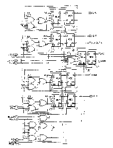
As shown in Figure 1 counter network 11 comprises a
plurality of registers (REG) 13, 15, 17, 19 and 21. Each
of the registers 13, 15, 17, 19 and 21 is preferably
formed as a D flip-flop, and may be implemented as Model
5F100151 flip-flops manufactured by Fairchild Camera and
Instrument Corporation.
The input to each of the registers are provided by an
associated multiplexer (MUX) 23, 25, 27, 29, and 31,
respectively, which may be implemented as Model F100171
multiplexers manufactured by Fairchild Instrument and
Camera Corporation. As is well understood by those
skilled in the art, the signal level output present at the
Z output of each of the multiplexers is clocked into the
associated register by the signal CLOCK, applied to the C
input to the register. Consequently, the signal level
present at the Z output of each of the multiplexers
appears at the Q output of the associated register
following the next CLOCK pulse. The time delay between
the appearance of a signal level at the multiplexer Z
output and the appearance of a corresponding signal at the
Q output of the associated register is determined by two
principal factors, i.e., the delay betwee. the appearance
of the multiplexer output and the occurrence of the next
succeeding clock pulse, and the internal propagation delay
of the register.
Each of the multiplexers 23, 25, 27, and 29 is
provided with a plurality of input ports I0, Il, I2, and
I3. The multiplexers are controllable to communicate the
signal on the selected one of the four input ports to the
Z output of the multiplexer, in response to the control
signals S0 and Sl. Control signals S0 and Sl are
generated by logic circuitry 31 in response to the
externally generated signals SELECT, HOLD and PEN, as set
forth below at Tables II, III and IV. Logic circuitry 31
is operative to translate the SELECT, HOLD, and PEN
.. . . .
- , ~: ............ - . . ..... .. : . .
' ' ' ' ' ' ' , . : :, . , .. . . . ^ ~ .; , .
791V~ .
--10--
signals into appropriate S0 and Sl signals for selecting
the proper input in response to the external signals.
Logic circuits 33, 35, 37, 39 and 41 comprise counter
enabling circuitry operative to sequentially provide an
input to the port, I0, of multiplexers 29, 27, 25, 23 and
31, respectively, when network 11 is operated in a
counting mode. Counter enabling circuitry 33, 35, 37, 39
and 41 cooperate with the multiplexers and registers to
sequentially generate output signals from registers 19,
17, 15, 13, and 21, respectively, upon the occurrence of a
predetermined number of clock pulses. Upon proper
sequencing of registers 19, 17, 15, and 13, register 21 is
enabled, ultimately resulting in the generation of a
terminal clock signal TC at the Q output of register 21.
Timing circuitry 41 is preferrably formed as an
or/nor gate connected to the complementary outputs (ZN) of
multiplexers 23, 25, 27, and 29. Connection to the ZN
outputs causes counter enabling circuitry 41 to
communicate an enable signal to the D input of multiplexer
- 20 31 when all of the ZN terminals are in a zero state, i.e.
upon the occurrence of the clock pulse preceding -the clock
pulse generating the terminal count signal~ Consequently,
the Z output of multiplexer 31 and, therefore, the D input
to register 21, are enabled in reponse to the clockpulse
immediately preceeding the clock pulse thc~_ generates the
terminal count signl. Upon the occurrence of the next
CLOCK pulse the register 21 is caused to generate a
terminal count (TC) signal. By use of counter enabling
circuitry 41 a looX ahead terminal count scheme is
affected such that the generation of the terminal count
signal TC is delayed beyond the occurrence of the
corresponding clock pulse signal by only the time
corresponding to the propagation delay inherent in the
opexation of register 21. It is to be understood that by
varying the circuitry used to form counter enabling
circuitry 41, or the connections thereto, a similar look
.
1~79~38
ahead terminal count scheme may be affected to correspond
with the generation of a terminal count signal in response
to any predetermined number of clock pulses.
Moreover, the inclusion of register 21 prevents the
generation of false terminal count signals where counter
enabling circuitry 41 generates a terminal count enable
signal at the I0 port of multiplexer 31 in response to
transient conditions of multiplexers 23, 25, 27 and 29.
For example, as network 11 transitions from a count of 1101
to 1110 there may be a brief moment where the count will
appear as 1111, resulting in a 0000 input to counter
enabling circuitry 41 and the consequent generation of a
terminal count enable signal to be communicated to the I0
port of multiplexer 31. Where network 11 is in the
counting mode this condition results in communication of a
terminal count enable signal to the input to register 21.
However, register 21 operates to isolate such transient
conditions from the output of network 11 and will only
generate an output when the register is enabled at the time
a CLOCK signal is received. By that time, the transient
conditions should be dissipated and the multiplexers should
all be transitioned to their correct stat . As will be
recognized by those skilled in the art, the CLOCK rate
should be selected with those transient conditions in mind
and should allow sufficient time for the circuit components
to complete transitioning between CLOCK pulses.
The present invention permits the counter network 11
to be tested without sequencing the registers and
associated combinational logic through the entire network
cycle. By controlling the state of S0 and S1, the test
pattern input from the SI terminal can be input to
multiplexer 23, and serially commmunicated through the
remaining multiplexers and registers independent of the
rate at which the terminal count signal is generated.
.... . . . . .. . .. ..
1;~7~
-12-
In the presently preferred embodiment a test pattern
may be communicated from the serial input port (SI) to the
test input port (I2) of multiplexer 31. When S0 and Sl
are at appropriate levels each of the multiplexers 23, 25,
27, 29 and 31 will operate to output the signal present on
the I2 input port of each associated multiplexer. That
signal is then communicated to the D input port of the
associated register. The signal is then communicated to
the Q output port of that register and is, in turn,
communicated to the I2 input port of another multiplexer.
Thus, the output of register 21 is communicated to the I2
port of register 23. That signal is then communicated to
the output of regiser 13 and then to the I2 input port
register 25. The same signal is communicated to register
15 and then to the I2 input port of multiplexer 27. The
output of register 17 is similarly communicated to the-I2
input port of multiplexer 29. The output of multiplexer
29 is communicated to register 19 from which a serial
output of the test pattern is discharged from terminal
Q(l). Thus, the test pattern input to network 11 at
terminal SI is serially communicated through each of the
multiplexers and registers and is ultimately output from
terminal Q(l). As noted above the rate at which the input
test pattern is communicated through the multiplexers and
registers is independent of the operation of the counter
enabling circuitry 33, 35, 37, 39, and 41. Accordingly,
all multiplexers and registers may be tested in a
convenient and expeditious manner, independent of any
interconnected combinational logic or the rate at which
the terminal count (TC~ signal is generated, i.e. the
network cycle time.
As shown at Figure 1 test pattern outputs may also be
obtained at terminals Q(2), Q(3), Q(4), and TC. Thus, the
operation of each multiplexer and register pair may be
independently checked. It should be noted, however, that
failures may be resolved to a specific register using the
.. . . . . . .
.... ~ . . .
9~
-13-
serial output by shifting in predetermined data patterns,
operating in count mode, shifting data through the
network, and comparing the output to expected levels.
In addition to communicating the output of each
register to the I2 input port of an unassociated
multiplexer, the output of each register is also
communicated to the Il input port of the associated
multiplexer. Upon the generation of appropriate S0 and Sl
control signals (see Tables II, III and IV) each
multiplexer is operative to communicate the signal
appearing on the Il input port to the associated register.
Thus, the output of that register is maintained at its
current level until the S0 or Sl signals change, or until
the register is reset.
Counter network 11 may also operate to parallel load
a plurality of data bits. In the presently preferred
embodiment a plurality of data bits may be communicated to
counter network 11 on the P terminal and communicated to
multiplexers 23l 25, 27, and 29 at the I3 input ports of
those multiplexers. Upon the appearance of appropriate
PEN, SELECT and HOLD signal levels, the information
appearing at the I3 input ports is communciated to the
associated registers and ultimately output from the
registers at the Q(l), Q(2), Q(3) and Q ~) terminals to
external circuitry. Counter enabling circuitry 33, 35,
37, 39, 41, register 21 and multiplexer 31 need not be
used when the network 11 is disposed in the parallel load
mode. When terminal count is parallel loaded into
registers 13, 15, 17 and 19, a terminal count output
signal is generated by register 21 in response to the same
clock pulse used to parallel load the registers.
As mentioned above, network 11 may be used to
facilitate checking the operation of external
combinational logic connected to network 11. Where the
output of some external combinational logic is
communicated to the I3 input ports o~ the multiplexers for
:,, ~
910
-14-
parallel loading, network 11 may be operated to input a
limited amoun-t of data from the external combinational
logic, and then operated in a test mode to serially output
the data trapped in the registers. Thus, the output of
the external combinational logic can be held and serially
output for comparison against expected levels. The
operation of the external combinational logic may
therefore be tested vis-a-vis the counter testing
circuitry of network 11.
If desired, a plurality of counter networks 11 may be
cascaded e.g., to facilitate higher order counts. In such
a cascaded network the complementary terminal count signal
(TCN) from the first stage serves as the complementary
terminal count prior signal (TCPN) to the second stage.
Similarly, the complementary look ahead output signal (LA
OUT N) from the first stage serves as the complementary
look ahead input signal (LA IN N) to ihe succeeding stage.
Similarly, the serial output signal from the Q(l)
terminal of the first stage may be used as the serial
input signal (SI) to the following stage. Thus, any
number of stages may be cascaded without the need for
external logic.
As previously discussed, various modifications,
additions and substitutions may be effectQd to implement
the structure and function of the component portions
without departing from the spirit and scope of the
invention. For example, other counter enabling circuitry
and various alternate multiplexing schemes may be utilized
to implement various counting schemes or interface various
combinational logic circuitry within the scope of the
invention. Additionally, it is clearly anticipated that
the present invention may have application in various
areas beyond those specifically addressed.
003a
.. ..
. . _
~L~t79~0~
-15-
Referring to Figure 2, another embodiment of a
look ahead terminal counter 56 is illustrated for
generating a terminal count output signal upon the
occurrence of a predetermined number of clock pulses. The
counter 56 is operative to reduce or eliminate sp~rious
output signals resulting from transient conditions present
at the counter registers. As with the circuit illustrated
at Figure 1, the counter 56 functions to isolate the
output signal (TC) from spurious conditions and reduces
delay time between the occurrence of the clock pulse
generating the terminal count signal and the generation of
the counter terminal count signal.
Counter 56 is formed of a plurality of counter
registers 51, 53, 55, and 57. As will be recognized by
those skilled in the art counter registers 51, 53, 55 and
57 may be formed of any of a number of commercially
available registers such as the Model F100151 flip-flops
manufactured by Fairchild Camera and Instrument
Corporation. Each of the registers has an input port
connected to counter enabling circuitry 59. The counter
enabling circuitry 59 may be similar to counter enabling
circuitry 33, 35, 37 and 39, illustrated at Figure 1, or
may be implemented to enable the registers in any of a
number of predetermined sequences e.g. bas- 3, 4, pseudo
random~ etc. Thus, after input of a predetermined number
of clock pulsPs to the registers 51, 53, 55 and 57, the
terminal count signal is generated and the counter cycle
repeats.
In accordance with the present invention, inputs
to the registers 51, 53, 55 and 57 are communicated to
output enable logic circuitry 61, which may be implemented
as a conventional AND gate. Logic circuitry 61 is
operative to generate an output enable signal in response
to predetermined conditions at the register input ports,
and to communicate the enable signal to the input port of
output register 63. The output register 63 is thus
, . ., . ~ . - . . . - - - . ; . .
~ ~79~
-16-
operative to generate a terminal count signal (TC) each
time the counter 56 reaches the desired state.
Moreover, the terminal count enable signal
output from enable logic circuitry 61 is isolated from the
output TC by register 63. The output signal from logic
circuitry 61 is communicated to the input of register 63
and the terminal count output signal is generated only
when an enable signal remains at the input to register 63
simultaneous with the occurrence of a clock pulse. The
output from logic circuit 61 is then used to trigger a
terminal count output signal, rather than being itself an
output signal, such that spurious output enable signals
due to transient conditions within the counter registers
and associated combinational logic will not result in
false terminal count signals. The delay between the
occurrence of the the terminal count clock pulse and the
generation of the terminal count output signal is
therefore limited to the inherent propagation delay of
register 63.
As will be apparent to those skilled in the art
various types of connecting schemes and combinational
logic may be used to implement output enable logic 61.
The central function of such logic being to generate a
terminal count enable signal to register ~3 sufficiently
prior to the occurrence of the terminal cc~nt clock pulse
such that spurious enable signals will dissipate prior to
the time that the terminal count clock pulse occurs.
~t791(38
-17-
TABLE II
Enablement of Operational Modes
SELECT HOLD FUNCTION
This is a counting or loading mode. If
PEN is inactive the counter synchronously
counts under the control of CEN. If PEN
is active the counter will synchronously
parallel load bits P(l) to P(4) where
P(4) is MSB.
Hold mode. The counter will be held in
its current state, i.e., Q(t+l) = Q(t).
Test mode. The counter will serial shift
from the SI line through all the
registers of the counter and out the
Q(l) line.
1 1 Set mode. The counter registers will be
synchronously set, e.g. to a zero state.
TABLE III
Selected Inputs to Multiplexers 23, 25, 27, 29
SELECT HOLD S0 Sl INPUT
(PEN = 0) (PEN 0)
0 1 1 I3
1 O 1 I 2
1 1 1 1 Io
.. .. . . . ...
.. _ . .... .. . ... , , , -- . , , . . ,, . _ _ . _ , . _ , . , . --~ -- , .
.. . . . .
.
9108
-18-
TABLE IV
Selected Inputs to Multiplexers 23, 25, 27, 29
SELECT HOLD S-0 1 INPUT
0 0 (PEN = 1) (PEN = 1) Io
O 1 1 L -- I 1
1 1 _ _ ~ = __ __ I 2
003b
..
'', , . '. "