Note : Les descriptions sont présentées dans la langue officielle dans laquelle elles ont été soumises.
1~793~i7
PROTECTION CIRCUIT FOR A THYRISTOR CONVERTER
BACKGRO~ND OF THE INVENTION
Field of the Invention
The present invention relates to a protection
circuit for a thyristor converter of which unit arm is
composed of a plurality of thyristors connected in series
with each other.
Descri~tion of the Prior Art
High-voltage thyristor converters are employed in
various applications such as direct-current power
transmission systems and reactive power compensation
devices. They accomplish their ratings by series or
series-parallel connection of many thyristors. Thus one
15 of technical problems with a thyristor converter of this
type is how to cause its respective thyristors to share
voltage and current stresses equally at the time of turn-
on or turn-off of the thyristors. To this end, various
measures are employed. Among these important technical
20 problems there is the problem of an over voltage due to a
partial turn-off at the time of turn-off (voltage share
among some of the series connected thyristors which are
turned off). In more detail, when many thyristors are
turned off, reverse voltages are required to be applied
25 across the corresponding thyristors during enough
intervals in order that all of the thyristors can
withstand forward voltages applied subsequently thereto.
In case these reverse voltage intervals are insufficient,
when a forward voltage is applied across the thyristors,
some thyristors can withstand the forward voltage, but
the remaining thyristors fail to perform forward
recovery, i.e., recover their features to withstand the
forward voltage, with the result that they maintain their
conductive states. This phenomenon is a so-called
35 partial turn-off phenomenon. When the turn-off
phenomenon occurs, the arm total voltage is applied
across some thyristors which have performed their Eorward
2 17~936~
recovery. Thus when the voltage applied across the
respective thyristors are approximately equal to or
higher than the rated voltage for the respective
thyristors, the corresponding thyristors ~1ill be broken
over to be fired ~ithout any gatin~ signal, and khus the
thyristors themselves or the converter will be broken.
Thus the prior art protection is that when the reverse
voltage interval (margin angle) ~t after conducting is
smaller than a predetermined value (set ti~e tS), Eiring
instructions are given forcedly to all the thyristors
(forced firing) to cause them to be fired simultaneously
in order to avoid application of over voltages across
some thyristors. Whether or not the reverse voltage
interval (margin angle) ~t is sufficient compared to the
predetermined value is determined in relation to the
turn-off time t~ of thyristor. On the other hand, since
this turn-off time tf is affected by the junction
temperature of the thyristor, the current reduction rate
of the thyristor before the reverse voltage interval, the
zo forward voltage increase rate of the thyristor, the value
of the forward voltage across the thyristor, etc., the
worst conditions, i.e., maximum value is employed as the
turn-off time tf.
A protection gating instruction signal is prepared
on condition that the reverse voltage interval at is
shorter than its set time tS to deliver it to all of the
thyristors, thus to forcedly fire them. In this case,
since the converter operates as an inverter, when viewed
from the entire system, it can be said that the converter
is forcedly brought into failure in commutation by forced
firing. Thus the system is adversely affected. Namely,
the protection of thyristors by forced firing is not
necessarily preferable for the system.
The set time tS is usually determined in relation to
the turn-off time tf (approximately 400 ~s) under the
worst conditions of the thyr~stor. Namelyr it is
determined to be approximately 600 to 800 ~s ~an
. -
3 ~ 3~
electrical angle of 10.8 to 14.4 degrees in the case of50 Hz) on the basis of the maximum value of the turn-off
time t~ in consideration of the phase difference due to
voltage unbalance and the set margin etc. In this
respect, when the direct current and its reduction ~ate
are not so large, i.e., when the commutation conditions
are not so severer the turn-off time tf can be 200 to 300
~15 .
The above prior art has the following drawbacks:
(1) Since the reverse voltage set time tS is set
under the worst operating conditions, the thyristor is
subjected to forced firing even when forced firing
protection is not required, for example, ~when the
junction temperature is low or current reduction rate of
the thyristor is small, thus allowing the converter to be
failed in commutation, resulting in the application of
the disturbance to the system.
(2) Since the reverse voltage set time t5 is
usually large; namely, 600 to 800 us (an electrical angle
of 10.8 to 14.4 degrees in the case of 50 Hz), constant
control of a control advance angle y in the inverter is
usually performed by setting the control advance angle at
a value larger than the reverse voltage set time tS, for
example, at an electrical angle of 15 to 17 degrees in
the case of 50 Hz in order to prevent frequent occurrence
of a protection gating signal. Suph a large control
advance angle would increase the reactive power of the
converter, with the result that reactive power larger
than is re~uired must be supplied for the system.
(3) Since the number of series connected thyristors
is ordinarily determined on the basis of the surge test
voltage in consideration of an inrush surge voltage (the
surge test voltage = (1.5 - 2.0) x the crest value of the
normal operating yoltage) instead of the normal operating
voltage, the converter can suEficiently withstand the
normal operating voltage when more than 50 to 70% (~1/2.0
- 1/1.5) x 100%) of the thyristors have perEormed their
~ 336~
forward recovery even if a partial turn-off phenomenon
would occur. Therefore, when at least more than 50% of
the thyristors have performed their forward recovery, the
occurrence of a protection gating signal, which would
adversely aEfect the system, i.e., commu~ation failure
should be avoided. In spite of this, since the prior art
protection frorn a partial turn-of~ due to an insufficient
margin angle is, in a sense, an anticipatory protection,
protection gating signals are produced more often than
they would be needed, giving rise to the serious drawback
for the system that commutation failure would be caused
unnecessarily many times.
The overvoltage prevention system for the partial
turn-ofE widely used in the prior art has been referred
to as abo~e. Another systern is proposed by the Japanese
patent publication ~o. 1865/77. In this system, forward
voltage sense circuits are provided one for each
thyristor to sense the individual forward voltages across
all of the thyristors in an analog manner. The
difference in voltage between two appropriate sets of
forward voltage signals output by the sense circuits is
extracted. Then, the voltage difference signal is
compared with a reference voltage corresponding to an
allowable forward~thyristor voltage (withstand voltage).
When the former exceeds the latter, it is judged that a
partial turn-off phenomenon has occur,red. On the basis
of this judgement, an operating signal is produced and
then is output via a pulse shaping circuit as a
protection gating instruction signal.
In accordance with this protection system, when a
partial commutation failure occurs actually, detection of
this fact is conducted to effect simultaneous firing for
protection. Accordingly, this allows unnecessary
simultaneous firing to be reduced to much extent as
compared with the first-mentioned system, thus making it
possible to lessen adverse influence on the system to
some degree. However, thls system also has the following
drawbacks:
(1) Two compared forward voltage signals are
considered in an attempt to select corresponding
thyristors having the maximum and minimum storage
carriers Qmax and Qmin. These Qmax and Qmin elements as
they are, however, will not necessarily be maximum and
minimum, respectively, under all of the operating
conditions, giving rise to the possibility the thyristors
cannot be protected. Namely, even if a partial turn-off
occurs, there could occur such a circumstance that the
detection of this partial turn-off is unable.
(2) Since the difference between the two forward
voltage signals (analog signals) corresponding to the
lS Eorward voltage across the thyristors is compared with a
reference voltage corresponding to a voltage near the
withstand voltage of a thyristor, there is no time margin
from the determination to the simultaneous firing,
resulting in the possibility that the thyristors may not
be protected. Namely, various partial turn-off states
are conceivable. Depending upon the number of elements
which cannot perform their forward recovery, the voltages
and voltage change rates of the elements which have
performed forward recovery vary to great extent. Thus it
is supposed that the thyristor voltages have already
exceeded their allowable values at the time when a
simultaneous-Eiring pulse i5 supplied thereto.
(3) Differently from the partial turn-off, the
partial turn-on is not necessarily caused by the
thyristors having the maximum storage carriers, i.e.,
short reverse voltage interval. In other words, even
among thyristors having the same storage carriers, the
thyristors having short turn-off time t~ are likely to
cause a partial turn-on.
Even the last mentioned prior art also fails to
perform a secure and safe protection at the time of
occurrence of the partial turn-off phenomenon.
1~:7~36~7
6 20375-579
SUMMARY OF THE INVENTION
It is an object of the present invention to provide a
protection circuit for a thyrlstor convçrter which can elimlnate
the above drawbacks, and ~hich can prevent commuta~ion ~ailure due
to unnecessary simultaneous ~iring as much as pos~ible, and
securely protect the thyristors when a partial turn-of~ phenomenon
has occurred.
According to the present invention, this and other
o~jects are accomplished by digitally detecting the
presence/absence of respective forward voltages across all of the
thyristors at a level low enouyh compared to the allowable
voltaye, judging how a partial turn-Qf~ ls conducted in accordance
with the number of detection signals indicative of the
presence~absence, and determining simultaneous firing protection
on the basls of the judgement.
Thus, in accordance with a broad aspect of the
invention, there is provided a protec~ion clrcui~ for a thyri~tor
converter of which unit arm is composed of a plurality of uni~s
connected in series, each unit including at leas~ one thyristor,
comprising 2
a plurality of forward voltage ~ense circuit mean~
provided in said respective units, for sensing an application of a
forward voltage~ when said ~orward vol~age is applied;
first means ~or detecting the time when said forward
voltage is applied across said unit arm on the basis Q~ output
signals from said forward voltage sens~ circult means;
second means for producing an operating æignal when more
than a predetermined number of said forward voltage sense circult
~7~3~7
6a 20375-579
means have sensed said forward volta~es; and
third means for simultaneously deliverlng a protection
gate firlng instruction to all of sald th~ristors o~ sald unit arm
on the basis of both ou~puts from said first and second means.
B IEF DESCRIPTION OF THE DRAWINGS
In the accompanying dr~wingss
Figure 1 ls a block diagram illustrating a firs~
embodiment of a protection circuit accordin~ to the present
invention;
Figure 2 is a timing chart used for explaining the
operation of the protection circuit o~ Figure l;
Figure 3 is a timing chart used for explaining the
operation of another embodiment of the protection circuit
according to the invention; and
Flgure 4 is a connection diagram of thyristor units in
still another embodiment of the protection clxcuit according to
the present invention.
DETAILED DESCRIPTION OF THE PREF~RRED EMBODIMENTS
Embodiment 1
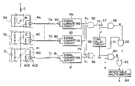
Figure 1 shows one embodimant of the present invention
in which a converter arm is composed of a thyristor connected in
series 11 to lN. In order to suppress the increase rate of a
thyristor current or voltage, a reactor 2 is connected in series
with the arm. These
7 ~ ;~7936~
thyristors 11 to lN are connected in parallel ~ith
voltage dividing circuits 31 to 3N, respectively, in
order that they share equally voltages applied across the
thyristors. When the converter arm constituted with
thyristors 11 to lM is divided into corresponding units,
these units are provided ~ith Eorward voltage sense
circuits 41, 42, ... 4N, respectively, each including a
resistor 401 having high resistance, a light emitting
element 402 connected in series ~ith resistor 401, and a
diode 403 connected in anti-parallel with light emitting
element 402. The sense level of each sense circuit
should preferably be as low as possible ~;ithin a range
where no unnecessary operation is effected. ~or example,
this sense level is set to a few percent of the crest
value of the operating voltage. The output signals from
the forward voltage sense circuits, i.e., light output
signals from light emitting elements 402, are delivered
via corresponding light guides 71 to 7N to the ground
potential sides and are then converted by corresponding
light receiving elements 81 to ~N and signal converting
circuits 91 to 9N to binary electric signals Pl to Pn.
These n forward voltage signals Pl to Pn thus obtained
are delivered to an AND gate 55 and an OR gate 56. The
output signal ca from tlle AND gate 55 is input via an
inverter 57 to a first input terminal of an ~ND gate 58.
To a second input terminal of the AND,gate 58, a singal d
obtained by passing the output signal co from OR gate 56
through a delay circuit 59 is input. The output signal
co from OR gate 56 is also input to a first input
terminal of an AND gate 60. To a second input terminal
of the AND gate 60, a conduction instruction signal b is
input. This conduction instruction signal b is delivered
via an inverter 61 to a first input terminal of an AND
gate 62. To a second input terminal of the AND gate 62l
an output signal e from the AND gate 58 is delivered.
Output signals f and g from the respective AND gate 62
and 60 are fed via an OR gate 63 to a monostable
8 ~7~
multivibrator 64 which outputs a gate instruction signal
h having a pulse width tp enough to fire the thyristors.
In accordance with the circuit shown in Fig. 1, the
AND output ca o all of the thyristor forward voltage
S signals obtained from the AMD gate 55 and the OR output
co of all of the thyristor forward voltage signals co
obtained from the OR gate 56 are logically compared to
judge the presence or absence of a partial turn-off
phenomenon. As a result, when it is judged that the
partial turn-off phenomenon is present, the above-
mentioned protection gating instruction signal f is
caused to be produced. Namely, according to the circuit
configuration of Fig. 1, in case no partial turn-off is
occurring the forward voltage OR signal co and the
forward voltage AND signal ca are detected substantially
simultaneously at the time when a forward voltage is
applied across the converter arm (t = t'2). In contrast,
in case the partial turn-off phenomenon is occurring, the
forward voltage OR signal co is detected at the time when
the forward voltage is applied across the arm (t = t'2)
since the thyristors which have performed their forward
recovery share the applied voltage. However, since there
are some thyristors which have not performed their
forward recovery, no forward voltage AND signal ca can be
detected. Thus this fact allows a partial turn-off to be
detected. This is the principle of the circuit shown in
Fig. 1.
Now the operation of the circuit of Fig. 1 will be
described in more detail with reference to the timing
chart of Fig. 2.
Fig. 2a shows the case where the reverse voltage
interval (margin angle ~t = t2 ~ tl) after the current is
turned off is sufficiently longer than the turn--off time
t of the thyristor and thus no partial turn-off occurs.
Fig. 2b shows the case where the reverse voltage interval
(~t = t'2 - t'l~ is shorter than the turn-off time tf and
thus a partial turn-off occurs In Fig. 2a, the
~. ~
9 ~7~3~:7
thyristors are turned off at time of t = tl, with the
result that the reverse voltage is applied across the
thyristors. Since the reverse voltage interval is
sufficiently long until time t = t2, no partial turn-of
occurs. At time t = tz, both forward voltage O~ signal
co and forward voltage ~lD signal ca are output. Since a
signal d delayed by a time td with respect to the forward
voltage OR signal co and a signal obtained by inverting
the forwârd voltage AND signal ca are input to the AND
gate 58, the output signal e of the gate 58 represents
logical 1l0ll and the output signal f of the AND gate 62
also represents "C". Namely, since no partial turn-off
occurs at this time, no protection gating instruction
signal is produced. On the other hand, in the case shown
in Fig. 2b, since the reverse voltage interval from time
t'l to t'2 is short, a partial turn-off occurs. As a
result, the forward voltage OR signal co shifts to
logical "1" at time t = t'2 when a forward foltage is
applied across the converter arm while the forward
voltage AND signal ca remains "0". Thus the AND
condition on the output d of delay circuit 59 and an
inverted signal the forward voltage AND signal ca holds
at time t = t'2 -~ td and thus the output signal e and
hence the gating instruction signal f become "1".
~5 Namely, at time t = t'2 + td~ the protection gating
instruction signal is produced and this signal is
delivered simultaneously to all of the thyristors. Thus,
the thyristors are rapidly protected against their
overvoltage condition during the partial turn-off. In
this case, since the forward voltage sense level is
sufficiently low, it is possible to judge the
presence/absence of a partial turn-off near a zero
forward voltage. In addition, since the voltage applied
across the thyristors when the thyristors are all fired
simultaneously are sufficiently low, the satisfactory
protection of the thyristors can be achieved. The delay
time td of delay circuit 59 is set in order to avoid
~7~t3~;7
unnecessary operations due to variations in the operation
of the respective orward voltage sense circuits. The
dalay time td is required to be set to about 10 to 100 ~s
although it depends upon the setting of the forward
S volt~ge sense circuits.
Embodiment 2
Instead of the AND gate 55 oE Fig. 1, an x/n logical
majority decision circuit 65 may be provided which
outputs a "1" signal when x or more of n forward voltage
sense signals are "1". In such a modification, even in
case all of the n -thyristors do not perform their forward
recovery, if x or more of the thyristors perform their
forward recovery with the (n - x) or less remaining
thyristors not performing their forward recovery, the
protection gating instruction signal can be locked.
Namely, it is assumed that if x or more of the thyristors
perform the forward recovery, the thyristors can
sufficiently withstand the steady-state converter arm
voltage. In such a case, although a partial turn-off
phenomenon is occurring, it is unnecessary to fire the
converLer arm forcedly, resulting in no possibility that
commutation failure is caused. In accordance with the
above concept, locking of the protection gating
instruction signal is implemented. In this case, x is
determined as the number of recovering thyristors enough
to cause them to cooperate to sufficiently withstand the
converter arm voltage, and thus usually as 50% or more of
the total number n. For example, when x is selected to
be 50% of n, the frequency of occurrence of protection
gating instruction signals can greatly be d~creased when
compared to the first embodiment (corresponding to x = n
= 100%). Assuming that n - 3~ x = 2, if two of three
forward voltage sense signals represent "1" at time t =
t2 in the case of Fig. 3a (corresponding to the case of
Fig. 2a), no protection gating instructlon signal is
produced. However, in the case of Fig. 3b (corresponding
to the case of Fig. 2b), since only one of all three
36~
Eorward voltage sense signals becomes "1" at time t = t'
2~ a protection gating instruction signal is produced at
time t = t 2 ~ td.
Other Embodiment
While a forward voltage sense circuit is sho~n as
being provided eor each thyristor in the embodiments 1
and 2, the present invention is not lirnited such an
implementation. In addition, there may be employed an
arrangement such that each unit includes, for e~ample, 2
to 10 oE thyristors connected in series and a forward
voltage sense circuit is provided per each unit. Fig. 4
illustrates forward voltage sense circuits 41, 42, ...
provided for units of paired thyristors 11, 12; 13,
14; ... respectively. Also, in this embodiment, a logic
circuit similar to that of the first and second
embodiments may be incorporated to obtain an operative
effect similar to those thereof. In this respect, in the
case of Fig. 1, it can be regarded that one unit is
constituted with a single thyristor~
While in the above embodiment, only a forward
voltage after a reverse voltage during normal commutation
in the converter has been described, it cannot be said
that a partial turn-off occurs necessarily in the normal
commutation alone. Such a partial turn-off can occur,
for example, when the bypass-pair operation is switched
to the normal operation or when the cgnducting thyristors
are turned off immediately after the gates are blocked..
As is clear from the description made thus far, the
present invention is also applicable during these partial
turn-off other than during commutation. While in the
above embodiments a forward voltage OR signal is used as
a time base signal, other equivalent signals may be used
instead. For example, either a zero voltage point signal
occurring when the reverse voltage transfers to the
forward voltage or a signal occurring when the reverse
voltage is lost may be used. In this case, however, it
is necessary to accurately correct the reference signal
12
and the time required for actual detection of a for~ard
voltage.
In the above three embodiments, each oE the
thyristors shown may be replaced with a plurality o
parallelly connected thyristors.
According to the present invention, a partial turn-
off phenomenon itself is detected and a protection yatiny
instruction signal is produced based thereon.
Accordingly, thyristors can securely be protected only
when they are truly in danger when compared with a
conventional, in a sense, anticipatory protection
depending upon the length of the reverse voltage
interval. Namely, when no partial turn-off is occurring
or when there is no danger although a partial turn-off is
occurring, there is no need for generation of a
protection gating instruction signal. The present
invention is capable of suppressing the occurrence of
such a unnecessary signal and the frequent generation of
unnecessary commutation failure. Thus conventional
constant control of a margin angle y having a value
larger than a set reverse voltage (margin angle) value
determined on the basis of a turn-off time of the
thyristor when the commutation conditions are severe, for
example, when the direct current is large or the current
reduction rate is high, can be reduced to the just limit
of occurrence of a partial turn-off dependlng upon the
commutation conditions according to the present
invention. Thus reactive pow r for the converter can be
reduced. In addition, according to the present
invention, it is assured that a partial turn-off of
detected and simultaneous firing voltage is sufEiciently
low, so that perfect protection of the thyristors is
accomplished.
:: . ,.~ . ;