Note : Les descriptions sont présentées dans la langue officielle dans laquelle elles ont été soumises.
~ ~'7''~
This application is a division of co pending
Canadian patent application Serial No. 516,944, entitled
FERROELECTRIC LIQUID CRYSTAL DEVICE, filed August 27,
1986.
The present invention relates to a liquid crystal
device for use in a liquid crystal display device, and
optical shutter array, etc., and more particularly to a
ferroelectric liquid crystal device having improved
display and driving characteristics, because of improved
initial alignment or orientation of liquid crystal
molecules.
Clark and Lagerwall have proposed the use o-f a
liquid crystal device having bistability (Japanese Laid-
Open Patent Application No. 107216/1981, U.S. Patent No.
4,367,924, etc.). As the bistable liquid crystal, a
ferroelectric liquid crystal having chiral smectic C
(SmC*) phase or H (SmH*) phase is generally used. The
ferroelectric liquid crystal has bistability, i.e., has
two stable states comprising a first stable state and a
second stable state, with respect to an electric field
applied thereto. Accordingly, different from the
conventional TN-type liquid crystal in the above-mentioned
device, the liquid crystal is oriented to the first stable
state in response to one electric field vector and to the
~5 second stable state in response to the other electric
field vector. Further, this type of liquid crystal very
quickly assumes either one of the above-mentioned two
stable states in reply to an
~;~'7~91~
--2--
electric field applied thereto and retains the state
in the absence of an electric field. By utilizing
these properties, essential improvements can be
attained with respect to the above~mentioned difficul-
ties involved in the conventional TN-type liquid
crystal device.
In order to provide a uniform orientation or
alignment characteristic to a ferroelectric liquid
crystal in the above described type of device, there
has been known to apply a uniaxial alignment treatment
onto a substrate surface. More specifically, the
uniaxial alignment treatment includes a method of
rubbing a substrate surface with velvet, cloth or
paper in one direction, or a method of obliquely
depositing SiO or SiO2 on a substrate surface.
sy applying an appropriate uniaxial alignment
treatment to a substrate surface, a specific bistable
eondition has been provided as an initial alignment
characteristic. Under such an initial alignment
condition, however, there have been.observed practical
problems such as poor contrasts and low light-
transmittances during an optical modulation test
earried out by using polarizers arranged in cross
nicols in combination with the device.
~More specifically, in a ferroelectric liquid
erystal device of the type deseribed above, a state
wherein molecules of a liquid crystal (hereinafter
9~
--3--
sometimes abbreviated as "LC") are twisted from an
upper substrate to a lower substrate in an LC molecular
layer (twis-t alignment state) as shown in Figure 21 is
readily developed rather than a state wherein LC
molecules are aligned in parallel with each other in
an LC molecular layer (parallel alignment state) as
shown in Figure 22. Such a twist alignment of LC
molecules leads to various disadvantages for a display
device such that the angle formed between the LC
molecular axes in the first orientation state and the
second orientation state (tilt angle) is apparently
decreased to result in a decrease in contrast or light
transmittance, and an overshooting occurs in the
response of the LC molecules at the time of switching
between the orientation states to result in an observ-
able fluctuation in light transmittance. For this
reason, it is desired that the LC molecules are placed
in the parallel alignment state for a display device.
2 0 SUMMARY OF THE INVENTION
The present invention has been accomplished to
solve the above mentioned problems and aims at provid-
ing a liquid crystal device improved in display
characteristics by realizing the parallel alignment
state of llquid crystal molecules.
We have observed that the above mentioned twist
alignment state can be transformed into the parallel
1~7~9~
alignment state by applying an appropriate alternating
voltage (hereinafter sometimes represented by an AC
voltage for parallel alignment) to a bistable ferro-
electric liquid crystal.
According to the present invention, there is
provided a ferroelectric liquid crystal device compris-
ing a pair of substrates each provided with an
electrode thereon, and a ferroelectric liquid crystal
layer disposed between the substrates in a thickness
which is thin enough to release the spiral structure
of the ferroelectric liquid crystal, wherein the
ferroelectric liquid crystal provides two average
molecular axis directions forming an angle 20 there-
between, each average molecular axis direction
corresponding to one of two stable orientation states
of the ferroelectric liquid crystal; the ferroelectric
liquid crystal provides two average molecular axis
directions forming an angle 2 ~ therebetween when
voltages exceeding the threshold voltage of the ferro-
electric liquid crystal are applied to the ferroelec~tric liquid crystal; and the ferroelectric liquid
crystal provides two average molecular directions
forming an angle 2~a therebetween after applying an
alternating electric fleld to the ferroelectric liquid
crystal and removing the electric field; the angles ~,
~ and Ha satisfying the relatlonship o: < ~a ~ ~ .
These and other objects, features and
:
79~
- 5
advantages of the present invention will become more
apparent upon a consideration of the following description
of the preferred e-mbodiments of the present invention
taken in conjunction with the accompanying drawings.
The following drawings and detailed description of
the invention relate not only to the ferroelectric liquid
crystal device which is the subject of the present
invention, but also to liquid crystal apparatus which is
claimed in co-pending Canadian patent application Serial
No. 516,944 of which the present application is a
division.
BRIEF DESCRIPTION OF THE DRAWINGS
Figure 1 is a schematic plan view for illustrating
an LC cell according to the present invention;
Figures 2 and 3 are a plan view and a sectional
view, respectively, of an LC cell;
Figure 4 is a circuit diagram for AC voltage
application;
Figures 5 and 6 are respectively a schematic view
for illustrating a ferroelectric liquid crystal cell;
Figures 7, 10, 12, 15, 17 and 20 are respectively a
circuit diagram of an example of the liquid crystal
apparatus according to the present invention;
Figures 8 and 11 are circuit diagrams of switches
used in the examples shown in Figures 7 and 10,
respectively;
Figure 9 is a sectional view showing another example
of the LC device according to the present invention;
Figures 13 and 18 are respectively a timing chart
for illustrating voltage signals used in an
1~'79'~
--6--
example of the present invention;
Figure 14 is an illustration of matrix picture
elements in an embodiment of the present invention;
Figures 16 and 19 are circuit diagrams of the
final stages of the driver circuits in the apparatus
shown in Figures 15 and 17; and
Figure 21 and 22 are respectively a schematic
view of projection of C directors on a chiral smectic
molecular layer in a twist alignment state and in a
parallel alignment state, respectively.
DESCRIPTION OF THE PREFERRED E~lBODIMENTS
Liquid crystal materials most suited for the
present invention are chiral smectic liquid crystals
showing ferroelectricity. More specifically, liquid
crystals showing chiral smectic C phase (SmC*), G phase
(SmG*), F phase (SmF*), I phase (SmI*) or H phase
(SmH*) are available.
Details of ferroelectric liquid crystals are
described in, e.g., "LE JOURNAL DE PHYSIQUE LETTERS"
36 (L-69) 1975, "Ferroelectric Liquid Crystals";
"Applied Physics Letters" 36 (11) 1980, "Submicro
Second BLstable Electrooptic Switching in Liquid
Crystals"; "Kotai Butsuri (Solid State Physics)" 16
(141) 1981, "Liquid Crystals", etc. In the present
invention, ferroelectric liquid crystals disclosed in
these publications may he used.
'7~3~3~
--7--
Examples of ferroelectric liquid crystal
compounds include decyloxybenzylidene-p'-amino-2-
methylbutyl cinnamate (DOBAMBC), hexyloxybenzylidene-
p'-amino-2-chloropropyl cinnamate (HOBACPC), 4-o-
(2-methyl)-butylresorcylidene-4'-octylaniline (~BRA 8),
etc. Especially preferred class of chiral smectic
liquid crystals used in the liquid crystal device
according to the present lnvention are those showing
a cholesteric phase at a temperature higher than the
temperature for giving a smectic phase. A specific
example of such chiral smectic liquid crystal is a
biphenyl ester type liquid crystal compound showing
phase transition temperatures as shown in an example
described hereinafter.
When a device is constituted using these
materials, the device may be supported with a block of
copper, etc., in which a heater is embedded in order to
realize a temperature condition where the liquid
crystal compounds assume a desired phase.
Referring t!o Figure S, there is schematically
shown an example of a ferroelectric liquid crystal cell
for explanation of the operation thereof. An example
where an SmC* phase constitutes a desired phase is
explained. Reference numerals 51 and 51a denote base
plates (glass plates) on which a transparent electrode
- of, e.g., In2O3, SnO2, ITO (Indium-Tin-Oxide), etc.,
is disposed, respectively. A liquid crystal of an
~,7~391~
SmC*-phase in which liquid crystal molecular layers 52
are aligned perpendicular to surfaces of the glass
plates is hermetically disposed therebetween. A full
line 53 shows liquid crystal molecules. The liquid -
crystal molecules 53 continuously form a helical struc-
ture in the direction of extension of the base plates.
The angle formed between the central axis 55 and the
axis of a liquid crystal molecule 53 is expressed as
~ . Each liquid crystal molecule 53 has a dipole
moment (Pl) 54 in a direction perpendicular to the
axis thereof. When a voltage higher than a certain
threshold leve] is applied between electrodes formed
on the base plates 51 and 51a, a helical structure of
the liquid crystal molecule 53 is unwound or released
to change the alignment direction of respective li~uid
crystal molecules 53 so that the dipole moments (Pl)
54 are all directed in the direction of the electric
field. The liquid crystal molecules 53 have an
elongated shape and show refractive anisotropy between
the long axis and the short axis thereof. Accordingly,
it is easily understood that when, for instance,
polarizers arranged in a cross nicol relationship,
i.e., with thelr polarizing directions crossing each
other, are disposed on the upper and the lower surfaces
of the glass plates, the liquid crystal cell thus
arranged eunctions as a liquid crystal optical modula-
tion device of which optical characteristics vary
~;~799~
_9_
depending upon the polarity of an applied voltage.
The liquid crystal layer in the liquid crystal
device of the present invention may be rendered
sufficiently thin in thickness (e.g., less than 10 ~).
5 As the thickness of the liquid crystal layer is
decreased, the helical structure of the liquid crystal
molecules is loosened even in the absence of an
electric field whereby the dipole moment assumes
either of the two states, i.e., P in an upper direction
64 or Pa in a lower direction 64a as shown in Eigure 6.
One half of the angle between the molecular axis 63 and
the molecular axis 63a is referred to as a tilt angle
~ , which is the same as half the apical angle of the
cone of the helical structure. ~Ihen an electric field
lS E or Ea higher than a certain threshold level and
different from each other in polarity as shown in
Figure 6 is applied to a cell having the above-
mentioned characteristics, the dipole moment is
directed either in the upper direction 64 or in the
lower direction 64a depending on the vector of the
electric field E or Ea. In correspondence with this,
the liquid crystal molecules are oriented in either
of a first stable state 63 and a second stable state
63a.
When the above-mentioned ferroelectric liquid
- crystal is used as an optical modulation element, it
is posslble to obtain two advantages as briefly touched
9~L~
- 1 0 -
on hereinbefore. First is that the response speed is
quite fast. Second is that the orientation of the
liquid crystal shows bistability. The second advantage
will be further explained, e.g., with reference to
Figure 6. When the electric field E is applied to
the liquid crystal molecules, they are oriented in
the first stable state 63. This state is stably
retained even if the electric field is removed. On
the other hand, when the electric field Ea of which
direction is opposite to that of the electric field
E is applied thereto, the liquid crystal molecules
are oriented to the second stable state 63a, whereby
the directions of molecules are changed. This state
is similarly stably retained even if the electric
field is removed. Furtner, as long as the magnitude
of the electric field E or Ea being applied is not
above a certain threshold value, the liquid crystal
molecules are placed in the respective orientation
states. In order to effectively realize high response
speed and bistability, it is preferable that the
thickness of the cell is as thin as possible.
The most serious problem encountered in form-
ing a device using such a ferroelectric liquid crystal
has been, as brie1y mentioned hereinbefore, that it
is difficult to form a cell having a highly uniform
monodomain wherein liquid crystal layers having an
SmC* phase are aligned perpendicular to the base plate
-1 1 -
phasea and the liquid crystal molecules are aligned
almost in parallel with the base plate phases.
There has been heretofore known a method of
applying a uniaxial orientation treatment to base -
5 plate surfaces when a large area of a liquid crystal
cell is produced. The uniaxial orientation treatment
is effected by rubbing the base plate surfaces with
velvet, cloth or paper in a single direction or by
the oblique or tilt vapor deposition of SiO or SiO2
onto the base plate surfaces. However, such a uni-
axial orientation treatment as by the rubbing or the
oblique vapor deposition has been considered in-
appropriate for a ferroelectric liquid crystal since
such an orientation treatment ~ se hinders the
bistability of the liquid crystal, based on which
driving utllizing a memory characteristic is realized.
According to our further study, it has been
found possible to provide a specific bistable state
as described hereinafter by applying a suitable uni-
axial orientation treatment to base plate surfacesand by arranging a polarizer in the specific axis
direction to realize driving effectively utilizing
a memory characteristic.
Figure 1 is a schematic view illustrating
molecular orientation states in a liquid crystal device
- according to the present invention. Figure 2 is a
plan view of an example of a liquid crystal cell used
-12-
in the present invention and Figure 3 is a sectional
view of the cell taken along the ]ine III-III shown
in Fi~ure 2.
Referring to Figures 2 and 3, an LC cell 1 -
comprises a pair of substrates 3a and 3b of glass or
a plastic, respectively provided thereon with stripe
electrodes 4a and 4b of 1000 A-thick ITO (Indium Tin
Oxide) stripe electrode films and further thereon with
alignment films 5a and 5b of 10 A - 1 ~m, preferably
O O
100 A ~ 5000 A, in thickness. Between the alignment
films are disposed polyimide spacers of 1 ~-dot shape
so as to retain the liquid crystal layer 2 in a
constant thickness over a wide area. The above
mentioned two substrates, after having been subjected
to a rubbing treatment, are secured to each other to
form a cell into which the liquid crystal is then
introduced.
Hereinbelow, an example wherein an ester type
liquid crystal mixture was used is explained with
reference to Figures 1 through 3. The ester-type
mixture liquid crystal showed the following phase
transition temperatures as determined by microscopic
observation:
Iso.(isotropic phase) 90C' Ch.(cholesteric phase)
75C' SmA (smectic A phase) 50CI SmC* below 0C'
Cry.(crystal phase)
9~
-13-
When the liquid crystal layer was formed in a
sufficiently large thickness (about 100 ~), the SmC*
phase assumed a helical structure and the pitch was
about 6 ~.
In the present invention, in order to realize
the parallel alignment state, it is desirable that at
least one of the alignment films 5a and 5b comprises
a polymer film having a polarity term ~YbP) of 20
dyne/cm or below, preferably 10 dyne/cm or below,
particula,rly preferably 7 dyne/cm or below.
According to our measurement, various polymer
films usable as alignment films showed the following
polarity terms:
Film speciesPolarity term (YbP)
po].yethylene2.6 dyne/cm
polyvinyl alcohol 3.3 dyne/cm
Nylon 12 3.7 dyne/cm
Nylon 11 5.0 dyne/cm
Nylon 2001 7.2 dyne/cm
Nylon 300111.5 dynelcm
polyimide*22.6 dyne/cm
*The polymide film was formed by a dehydro-
ring closure reaction at 300C of a coating film of a
polyamic acld which was a dehydro-condensation product
of pyromellitic dianhydride and 4,4'-diaminodiphenyl
ether.
The above mentioned values of polarity terms
-14-
are those measured according to a method described in
Nippon Settyaku Kyokaishi (Journal of Adhesion Society
of Japan) vol. 18, No. 3 (1972), pp. 131-141 under the
conditions of a temperature of 20C and a relative -
humidity of 55 %. The B-series liquids (containing
no hydrogen bonding component or dispersion component)
were 5 species of methylene iodide, tetrabromoethane,
~-bromonaphthalene, tricresyl phosphate, and hexa-
chlorobutadiene. The above values are respectively an
average of measured values obtained with the five
liquids.
Further, the above prepared 100 ~-thick cell
gave a spontaneous polarization of 10 nC (nano-
Coulomb)/cm2 at 25C as measured by the triangular-
wave application method (K. Miyasato et al., JapaneseJournal of Applled Physics 22 (10), p.p. 661-663
(1983), "Direct Method with Triangular Waves for
Measuring Spontaneous Polarization on Ferroelectric
Liquid Crystal"). There is a tendency that the
increase in tilt angle under the memory state by the
AC application according to the present invention may
be eas~ily accomplished for a liquid crystal having a
relatively large spontaneous polarization. For this
reason, a ferroelec tric liquid crystal having a
spontaneous polarization at 25C of 5 nC/cm2 ox larger,
particularly 10 nC/cm2 - 300 nC/cm2, is suited for the
present invention. The values, however, can vary
9~:31~
-15-
depending on the kinds of the alignment films.
The preparation procedure of a ferroelectric
liquid crystal cell 1 as shown in Figures 2 and 3 is
supplemented hereinbelow.
First, a cell structure 1 containing the above
mentioned biphenyl ester type liquid crystal is set in
such a heating case (not shown) that the whole cell 1
is uniformly heated therein. When, the cell. 1 is
heated to a temperature (about 95C) where the liquid
crystal in the cell assumes an isotropic phase. The
temperature of the heating case is decreased whereby
the liquid crystal in the cell 1 is subjected to a
temperature decreasing stage. In the temperature
decreasing stage, the liquid crystal in the isotropic
phase is transformed at about 90C into a cholesteric
phase having a grandjean texture and, on further
cooling, transformed from the cholesteric phase to an
SmA phase which is a uniaxially anisotropic phase at
about 75C. A-t this time, the axes of the liquid
crystal molecules in the SmA phase are aligned in the
rubbing direction.
Then, the liquid crystal in the SmA.phase is
transformed into an SmC* phase on further cooling,
whereby a monodomain of SmC* phase with a non-spiral
structure is formed if the cell thickness is of the
order of, for example, 3 ~m or less.
Referring again to Figure 1, the figure is a
9~
-16-
a schematic plan view illustrating the s-tate of orien-
tation of liquid crystal molecules as viewed from
above the substrate face 15.
In the figure, the two-head arrow 10 indicates
a direction of a uniaxial orientation treatment, i.e.,
the direction of rubbing in this embodiment. In the
SmA phase, liquid crystal molecules are oriented or
aligned in an average molecular axis direction 11 which
coincides with the rubbing direction 10. In the SmC*
phase, the average molecular axis direction of the
liquid crystal molecules is tilted to a direction 12,
so that the rubbing direction 10 and the average
molecular axis direction 12 forms an angle B to result
in a first stable orientation state. When a voltage
is applied between a pair of ~ase plates in this stage,
the average molecular axis direction of the liquid
crystal molecules in the SmC* phase is changed to a
saturation angle ~ larger than the angle B, where
a third stable orientation state is attained. The
average molecular axis direction at this time is
denoted by a reference numeral 13. When the voltage
is then returned to zero, the liquid crystal molecules
are returned to the former first molecular axis
direction 12. Accordingly, the liquid crystal mole-
cules have a memory characteristic in the state ofthe first molecular axis direction 12. When a voltage
of the opposite polarity is applied in the state of
~ ~7~391~1
-17-
the molecular axis direction 12 and the voltage is
sufficiently high, the average molecular axis direc-
tion of the liquid crystal molecules is shifted to
and saturated at a fourth stable orientation state
giving an average molecular axis direction 13a. Then,
when the voltage is returned to zero, the liquid
crystal molecules are returned to and settled at the
second stable state giving the average molecular axis
direction 12a. As a result, when the polarizing
direction 1~ of one polarizer is set in the same
direction as the molecular axis direction 12 forming
the angle 0, an optical contrast between an ON state
and an OFF state can be improved in a driving method
utilizing an orientation between the first and second
stable orientation states and the memory characteris-
tics.
The angle ~ is detected as an average of the
molecular axes in one stable state, and a reason for
the angle ~ being smaller than the angle ~ ~ay be
attributable to the fact that the liquid crystal
molecules are not aligned or oriented in completely
parallel with each other in an SmC* layer so that the
average molecular axis orientation provides the angle
~. It~ is;consldered possible in principle to have
the angle 0 be in concord with the angle ~ .
~ It is:very effective to increase the value of
for the purpose of transmittance of a liquid crystal
:: :
~L~t7~31
-18-
device. More specifically, in a liquid crystal device
utilizing the birefringence of a liquid crystal, a
transmittance with right angle cross nicols is deter-
mined by the following equation:
S I/Io = sin 4~ sin (~nd~/~) (1),
wherein Io denotes an incident light intensity, I a
transmitted light intensity, 0 a tilt angle, ~n a
refractive index anisotropy, d the thickness of a
liquid crystal layer, and ~ the wavelength of an
incident light. The above equation holds true with a
case wherein one polarization axis of the right angle
cross nicols is arranged to coincide with the average
molecular axis direction in one stable state and the
transmittance is obtained when the liquid crystal
molecules are re-oriented to the other stable state,
wherein the liquid crystal molecules are aligned in
completely parallel with the substrate faces. It has
been also confirmed, however, that the above equation
also holds true with a case wherein the molecular axis
directions providing the angle ~ are nearly paralLel
with the substrate faces. As a result, the maximum
transmittance is obtained at the tilt angle ~ = 22.5.
The measurement of the before mentioned ~, ~a
and ~ has been conducted in the following manner.
A pair of polarizers are disposed in right angle cross
nicols to sandwich a liquid crystal cell. A positive
s~3~L~
- 1 9 -
pulse exceeding the threshold voltage is applied across
the cell, and the cross nicol polarizers are rotated
with respect to the cell while retaining their relative
positions to a position where the darkest state of the
cell is reached. Then, a negative polarity pulse
exceeding the threshold voltage is applied to the cell,
and the cross nicol polarizers are again rotated until
the darkest state of the cell is again reached. The
rotation angles between the positions providing the
two darkest states thus measured for the respective
conditions correspond to twice the tilt angle 0, 0a
and ~ . Further to say, the tilt angles 0 and ~a are
those in the memory state, so that they are measured
after removal of the pulse voltages. On the other
hand, the tile angle ~ is measured while the pulse
voltages are applied. Specific examples of actual
measurement are explained hereinbelow.
Example 1
Two cells having a cell thickness _ of 1.1 ~m
2n and 1.8 ~m, respectively, were prepared by using a
polyimide film having a polarity term lybP) of 7.5
dyne/cm for both the alignment films 5a and 5b. The
tilt angles ~ were respectively measured at 8.0 and
7.5 which are both below the optimum value. Then,
two polarities of pulses respectively of DC 50 volts
were applied to the cells (d = 1.1 ~m and d = 1.8 ~m),
whereby the tilt angle ~ were respectively measured
79~33L~
-20-
at 23.1 and 24.0 which are close to the optimum
value.
Further, switching between the bistable states
was effected by using various magnitudes of voltage
pulses in combination with various pulse durations
with respect to the two cells, whereby the following
swiching voltages were obtained.
Table 1
lOPulse duration (m.sec) 1.5 1.0 0.5
d = 1.1 ~m) 10.1 V 10.1 V10.1 V
d = 1.8 (~m) 14.0 V 14.0 V14.0 V
Further, various AC voltages in the ranges of
~ F 150 V and 20 - 100 EIz were applied to the cells,
and after the removal of the voltages, the tilt angle
~a between the bistable states and the pulse duration
- voltage characteristics of pulses for switching
between bistable states~were again examined.
When the AC voltages were applied for 10
seconds, the following results were obtained. The
effective frequency range for increasing the tilt
angle ~ was 30 - 40 Hz and no remarkable difference
in effectiveness was observed in this range. At the
frequency of 40 Hz, no remarkable difference in -tilt
angle Oa was observed in the range of 10 - 50 V,
.,
~.~'799~
whereas in the range of 50 - 60 V, the domains of
~a = 21.0 and 0a = 18.8 be~an to appear for the all
thickness of d = 1.1 ~m and d = 1.8 ~m, respectively.
Further, in -the range of 60 - 150 V, the domains -
developed entirely to provide a very good contrast.
Over 150 V, however, the monodomains were disordered
and other defects were also observed.
Switching voltages after the application of
the voltage of 60 - 150 V were as shown in the
following Table 2 for switching between the bistable
states giving the tilt angle ~a.
Table 2
l5Pulse dur~t lOD (m.sec) 1.5 1.0 0.5
d = 1.1 (~m) 14.6 V 16.1 V 18.6 V
d = 1.8 (~m) 16.9 V 17.4 V 21.1 V
As is apparent from the above Table 2 in
comparison with Table 1, the parallel alignment state
giving the tilt angle 0a required higher switching
voltages than in the bistable state before the ~C
voltage application. This is considered to be because
the title angle ~a approached to ~ , so that it was
necessary to apply an energy for also inverting liquid
crystal molecules in the vicinity of the alignment
films to invite an inevitable increase in driving
~ ~'7
-22~
voltage for switching.
The transmittance given by the tilt angle Oa
after the AC voltage application increased to 14 % for
the cell thickness of d = 1.1 ~m and 19 % for d = 1.8
~m, which were nearly three times the values before the
AC application.
Example 2
The procedure of Example 1 was repeated except
that polyvinyl films having a polarity term YbP of
3.3 dyne/cm were used in place of the polyimide films
on the glass substrates and a cell thickness of
d = 1.5 ~m was adopted. Basically similar results as
follows were obtained.
Effective AC voltage: 45-70 V, 30~70 Hz
AC application time: 5 - 20 seconds
Tilt angle:
Before AC voltage application 0 = 7.8
During DC voltage application ~ = 22.8
After AC voltage application ~a = 21.6
Switching voltages were as shown in the follow-
ing Table 3.
Table 3
Pulse duration (m.secj 1.5 1.0 0.5
Voltage ~V) 16.2 17.0 21.4
:
.
-23-
The transmittance was 6 ~ before the AC voltage
application and 18 %, i.e., three times, after the
application.
Example 3
As described hereinbefore, a ferroelectric
liquid crystal phase having bistability is generally
produced through temperature decrease from another
higher temperature phase. In this example, the cells
used in Exa~ples 1 and 2 were cooled while applying
thereto an AC electric field of 40 V and 50 Hz,
whereby uniform monodomains of parallel alignment
states were realized over a wide area.
Example 4
A cell which has been transformed into a
parallel alignment state providing a high contrast
due to application of an AC electric field can return
to an original low contrast state after standing for
several days. Accordingly, when a ferroelectric liquid
crystal cell in a parallel alignment state providing
a tilt angle Oa is used for a display device, it is
necessary and effective to apply an AC voltage to the
cell before use thereof or when the contrast is lowered
during use. Figure 4 is a diagram for illustrating a
peripheral circuit for the above mentioned AC applica-
tion. Referring -to Figure 4, transparent electrodes
41 and 42 formed on a pair of glass substrates for
sandwiching a liquid crystal are disposed mutually at
~79~
-24-
right angles to form picture elements in the form of a
matrix. These electrodes 41 and 42 are connected to
driver circuits 43 and 44, respectively, for applying
voltages thereto. An AC voltage generator 45 is -
5 disposed selectively connectable to the electrodes 42.
More specifically, the driver circuit 42 and
the AC voltage generator 45 are connected to the
transparent electrodes through changeover switches
46. When the switches are closed to the driver cir-
cuit 44, image display signals are supplied to theelectrodes 42, whereas when the switches are closed
to the AC voltage generator 45, an AC voltage is
simultaneously applied to all the electrodes 42. In
this way, a ferroelectric liquid crystal is retained
in the alignment state providing the tilt angle ~a
in the present invention.
On the other hand, the driver circuit 43
supplies a constant voltage, e.g., 0 volt, to all the
electrodes 41.
Example 5
Figure 7 shows another example of circuit for
applying an AC voltage. Reference numerals 71 and 72
respectively denote transparent electrodes disposed
mutually at right angles to form matrix picture
elements and formed a pair of glass substrates sand-
wiching a llquid crystal. Numerals 73 and 74 respec-
tively denote driver circuits for applying voltages
9~
-25-
to the electrodes, and 75 an AC voltage generator.
Switches 76, 77, 78 and 79 are selectively
turned ON and OFF as required for AC application.
When the picture elements are driven in a desired
manner, the switches 76 and 77 are turned ON and
the switches 78 and 79 are turned OFF.
When an AC electric field is applied for
realizing the parallel alignment state, the switches
76 and 77 are turned OFF, and the switches 78 and 79
are turned ON. The switches 76 and 77 are turned OFF
in order to protect the driver circuits 73 and 74.
Figure 8 illustrates a circuit example for one electrode
line 71. Generally, the withstand voltage of a tran-
sistor is to a value of the order of a driving voltage.
However, the AC voltage applied through a line 80 is
required to be higher than an ordinary driving voltage.
For this reason, so as not apply a load exceed-
ing the withstand voltage to transistors 81a and 81b,
power supplies to the driver circuits 73 and 74 are
disconnected by means of one switch 76a among the
switched 76, whereby the driver circuits 73 and 74
are protected.
Example 6
The liquid crystal apparatus used in Example 5
requires a rather complicated switching mechanism. In
this example, in order to decrease the number of
switches, a two-layer electrode structure is adopted.
9~
-26-
A sectional view for this arrangement is shown
in Figure 9, in which numerals 90a and 90b denote
transparent substrates such as ylass plates, 91a and
91b matrix electrodes, and 92a and 92b whole area
electrodes covering the whole picture area. The whole
area electrodes 92a and 92b are insulated from the
matrix electrodes 91a and 91b by insulating films 93a
and 93b. The circuit arrangement of a liquid crystal
device having the two-layer electrode structure is
shown in Figure 10. The whole area electrodes 92a
and 92b are disposed so as to sandwich the matrix
electrodes 108 (combination of 91a and 91b). As in
Example 5, at the time of driving, an AC application
power supply 102 is turned OFF and switches 103 and
104 are turned ON. At the time of AC application, the
switches 103 and 104 are turned OFF and the AC power
supply 102 is turned ON. The switches 103 and 104
have a function of protecting driver circuits 105 and
106 from electrical damage and also a function of
electrically floating the inner matrix electrodes 108
to e~fectively apply an AC field supplied from the
whole area electrodes 92a and 92b outside the matrix
electrodes to the inner SmC* liquid crystal layer.
Figure 11 shows a driver circuit for one line
used in this example. In order that the electric
field applied from the whole area electrodes 92a and
92b outside the matrix electrodes 108 is effectively
~ ~ 7 ~ 9
-27-
applied to the liquid crystal layer, it is necessary to
place the matrix electrodes 108 by a switch 104a.
According to this example, the driver circuit
corresponding to the number of lines can be turned OFF
from the ground altogether by turning off the switch
104a, so that the switching mechanism can be simpli-
fied.
Example 7
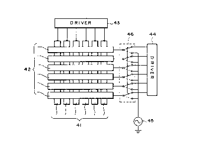
According to a system as shown in Figure 12,
driver circuits 121 and 122 can be completely isolated
from matrix electrodes 126 by switches 123 and 124, so
that the matrix electrodes are completely electrically
floated at the time of applying a voltage to whole
area electrodes. On the other hand, at the time of
driving, the AC circuit 127 is turned OFF. According
to this circuit arrangement, the driver circuits can
be protected from electrical damage when a high voltage
AC application is required.
Examples 8 - 11
Example 1 was substantially repeated while the
polyimide films on the glass substrates were respec-
tively replaced by polyethylene films (Example 8),
Nylon 12 films (Example 9), Nylon 11 films (Example 10)
and poLyimide films (Example 11), and the cell thick-
ness d was set to 1.5 ~m. The tilt angles ~a for the
respective cells after an AC appl.ication of 70 V and
70 Hz for 20 seconds. The results are summarized in
9~
-28-
the following table.
Example Alignment film (YbP) Tilt angle 0a
8 polyethylene (2.6 dyne/cm) 20.0
9 Nylon 2 (3.7 ~ ) 18.5 !''
510 Nylon 11 ~5.0 " ) 18.0
11 polyimide (22.6 " ) 8
Further, according to a preferred embodiment
of the present invention, there is provided a liquid
crystal apparatus comprising: a liquid crystal device
comprising matrix electrodes including scanning
signal lines and information signal lines spaced rom
and intersecting with each other, and a ferroelectric
liquid crystal material disposed between the matrix
electrodes; a scanning signal side liquid crystal
driver circuit, and peripheral circuits thereof
including a latch circuit and a shift register cir-
cuit; and an information signal side liquid crystal
driver circuit and peripheral circuits including a
latch circuit and a shift register circuit; wherein
the liquid crystal driver circuits, the latch circuits
and the shift register circuits are respectively of
the same structure on the scanning signal side and the
information signal side; and an alternating voltage is
simultaneously applied to all the picture elements
from at least one of the driver circuits.
In this embodiment, the AC voltage for parallel
alignment is provided as a combination of signals from
~ ~79~
-29-
the scanning signal side driver circuit and the infor~
mation signal side driver circuit having the same wave
height and frequency and reverse phases. After the
~C voltage application for parallel alignment, display -
signals corresponding to given image signals areapplied.
In this embodiment, the output stage transis-
tors constituting the scanning signal side driver
circuit and the information signal side driver circuit
are those having the same withstand voltage which is
equal to or above the waveheight of the AC voltage for
parallel alignment.
It is required that the AC voltage for parallel
alignment is such that liquid crystal molecules can
cause switching between bistable states while suffi-
ciently responding thereto. The voltage waveheight
thereof strongly depends on the kinds of liquid crystal
material and alignment film used and the frequency, and
may be adjusted to the same order as the waveheight of
pulse voltages for switching.
Driver circuits and peripheral circuits thereof
for a liquid crystal device in a matrix arrangement are
made symmetrical. In other words, so-called vertical
units and horizontal units of these circuits are made
of the same construction. By this arrangement, one
set of these may be used for the scanning signal lines
and the other may be used for the information signal
~L~79~
-30-
lines by only changeover switching, so that the verti-
cal writing and horizontal writing can be easily
switched. Furthermore, by similarly connecting two
driver circuits to driving power supplies, it is -
possible to apply an AC voltage for parallel alignment
from a driving power supply prior to writing pulses.
This embodiment is explained with reference to
the drawings.
Figure 14 shows an electrode arrangement for
a matrix display co~mprising scanning signal lines and
information signal lines forming picture elements at
respective intersections, and an example of display
formed at the picture elements.
In Figure 14, S1 - S5 denote scanning signal
lS lines and I1 ~ I5 denote display signal lines. It is
assumed that the hatched picture elements correspond
to a "black" writing state and the white picture
elements correspond to a "white" writing state.
Figure 13, especially at the display signal
application period, shows a timing chart for forming
a display state shown in Figure 14 accordlng to a
line-sequential writing mode wherein the scanning
signal lines S1 - S5 are line-sequentially scanned
and the columns of the information signal line I1 and
I2 are alternately written in "white" and "black". In
Figure 13, ~T denotes a writing pulse duration, and
it is assumud that a po~itive electric field is used
!
9~
-31-
for writing "white" and a negative electric field is
used for writing "black". It is also assumed that
writing pulses are those having a pulse durations of
~T and waveheights of ~3Vo exceeding the threshold. ~-
More specifically, Figure 13 corresponds to a
scheme wherein picture elements on a scanning signal
line are first written in "white" and selected picture
elements on the scanning line are then written in
"black" (line clear-line writing), and the information
signal includes a writing signal and an auxiliary
signal subsequent thereto for preventing a crosstalk
caused by continuation of the same polarity of signals.
Immediately after energization of the driving
circuits, as shown at the AC application period in
Figure 13, AC voltages for parallel alignment are
simultaneously applied to all the scanning signal lines
and the information signal lines with the same voltage
heights V', with rectangular waves of the same fre-
quency, but in antiphases. As a result, a rectangular
AC voltage of a waveheight 2V' is applied across the
substrates.
The AC voltage for parallel alignment is for
transforming liq~id crystal molecules from the twist
state into the parallel state, and the waveheight and
pulse duration thereof may be set to values respec-
tively exceeding those of the writing pulses. In this
examplej a writing pulses of 1 msec and 10V was used,
-32-
whereas a rectangular AC voltage of 50 Hz and about
20 V (Vpp.) was applied for several seconds to reali~e
the parallel alignment state.
The liquid crystal material used herein was a -
ferroelectric liquid crystal composition comprising,as the major components, p-n-octyloxybenzoic acid-p'-
(2-methylbutyloxy)phenyl ester and p-n-nonyloxybenzoic
acid-p'-(2-methylbutyloxy)phenyl ester. The liquid
crystal cell was prepared by providing an alignment
film of polyvinyl alcohol (PVA) on ITO pattern elec-
trodes on a pair of glass substrates, followed by
rubbing, and fixing to provide a cell thickness of
about 1.5 ~m. Between the transparent electrodes and
the alignment films, insulating films of SiO2 may be
inserted.
Figure 15 shows a circuit arrangement for a
liquid crystal apparatus according to the present
invention. In Figure 15, the same circuit arrangement
is used for both the scanning signal side and the
information signal side, wherein reference numeral
156 denotes a liquid crystal matrix panel, 157 an
information signal side driver circuit, 158-a scanning
signal side driver circuit, 159 and 150 latch circuits,
151 and 152 S/R (shift register) circuits, 153 a
driving power supply, 154 a driving voltage control
circuit, and 155 an I/F (interface).
In operation, when a main switch (not shown)
1.;~7~''3~
is first turned on, an AC voltage of Vs' is applied
to all the scanning electrodes and an AC voltage of
VI' of antiphases with Vs' is applied to all the
information signal electrodes respectively at a pulse --
duration of QT', so that a rectangular AC voltage of
VAc Vs' + VI' (peak-to-peak) is applied across the
upper and lower substrates as an AC voltage for
parallel alignment. After this AC voltage is applied
for a prescribed period to transform the liquid
crystal molecules into a parallel alignment state,
display driving signal voltages, i.e., a scanning
signal voltage of 3Vo and -2Vo and an information
signal voltage of +V0 both having a pulse duration of
~T, are set by a driving voltage control circuit 154,
and a multiplex driving is started depending on input
signals DH.
Further, switching between the horizontal
writing and the vertical writing may be easily effected
by changing switches SW 16 - 18 depending on a H/V
switching signal 160 to exchange the scanning signal
side and the information signal side.
Figure 16 shows a circuit structure at the
final stage of the driver circuit 157 or 158 shown in
Figure 15. Tx1 and Tr2 denote output stage transis-
tors. Referring to the driving waveform shown in
- Figure 13, the withstand voltages Vc of the two output
stage transistors are equally set to satisfy the
;
.
~ ;~'7~
-3~~
following relationship:
Vc > V (Vs ~ VI ) = V0
Further, by appropriately selecting -the liquid
crystal material, the kind of the alignment film, and --
the frequency of the AC voltage for parallel alignment,it is possible in this embodiment to satisfy the
following relationship.
Vc > V' ~ VO.
Anyway, as the two driver circuits 157 and 158
are equally connected to the driving power supply 153,
an AC voltage for parallel alignment having a wave-
height and a pulse duration equal to or larger than
those of the writing pulses as shown in Figure 13 may
be applied between V+ and V_ terminals shown in Figure
lS 16 prior to the input of a display signal DH' shown in
Figure 16 to accomplish the parallel alignment of the
liquid crystal.
According to another preferred embodiment of
the present invention, there is provided a liquid
crystal apparatus comprising: a liquid crystal device
comprising matrix electrodes including scanning signal.
lines and information signal lines spaced from and
intersecting with each other, and a liquid crystal
material disposed between the matrix electrodes, each
intersection of the scanning signal lines and the
information signal lines in combination with the
liquid crystal material disposed therebetween
~'7~9~
-35-
constituting a picture element, a scanning signal side
driver circuit, and an information signal side driver
circuit; the liquid crystal apparatus being so con-
structed that an alternating voltage is applied to the -
whole picture elements prior to application of displaysignals according to a multiplex driving scheme.
In this embodiment, the application of display
signals and the application of an AC voltage for
parallel alignment are controlled by a common driving
power supply circuit. The application of the AC
voltage for parallel alignment may be effected by
selecting either of the two methods, one of which
comprises applying the ~C voltage from either one of
the scanning signal side driver circuit and the infor-
mation signal side driver circuit and grounding theother side of signal lines all together during the
AC voltage application period, and the other of which
comprises AC voltages of mutually antiphases from the
scanning signal side driver circuit and the information
signal side driver circuit.
The AC voltage for parallel alignment may for
example be a rectangular waveform of alternating
polarities, the voltage waveheight of which may be
set to a value higher than the voltage of display
signals required for switching of the liquid crystal
in the parallel alignment state.
Thus, according to this embodiment, liquid
3~
-36-
crystal driver circuits each connected to the scanning
signal side and the information signal side are
eonnected to a common driving power eircuit, and the
display signal voltages and the AC voltage for parallel ~~
alignment are applied from the driving power supply
eireuit. More speeifieally, prior to multiplex driving
using display signals, an AC voltage of, e.g., reetan~
gular pulses having desired waveheight and pulse
duration is applied to preliminarily plaee the liquid
erystal in a parallel alignment state, and then the
liquid erystal driving for display is started.
Figure 17 shows an example of liquid crystal
apparatus for supplying signal voltages as shown in
Figure 18.
In Figure 17, referenee numeral 171 denotes
an interface (I/F), 175 denotes a shift register (S,/R)
eireuit, 176 a lateh eireuit, 177 an information signal
side driver circuit, 178 a scanning signal side driver
eireuit, and 179 an LC matrix panel. A driving power
supply eireuit 170 comprises a driving power supply
170a and a driving voltage control eireuit 170b.
In operation, when a main switch (not shown)
is first turned on, AC voltages for parallel alignment
having waveheights V5' and ~I' and a pulse duration ~T'
are applied in mutually antiphases to all the seanning
eleetrodes and the information signal eleetrodes,
respeetively, so that a reetangular AC voltage of
9~
VAc (peak-to-peak3 = Vs' + VI' is applied across the
upper and lower substrates. After this AC voltage is
applied for a prescribed period to transforrn the liquid
crystal molecules into a parallel alignment state, -
dispaly driving signal voltages, i.e., a scanning
signal voltage of 3Vo and -2Vo and an information
signal voltage of +V0 both having a pulse duration of
~T, are set by a driving voltage control circuit 154,
and a multiplex driving is started. The waveheights
Vs', VII and the pulse duration aT' of the AC voltage
for parallel alignment are larger than the waveheight
3Vo, V0 and the pulse duration ~T, respectively, of
the writing pulses.
Figure 19 shows a circuit structure at the
final stage of the driver circuit 177 or 178 shown in
Figure 17. Tr1 and Tr2 denote output stage transis-
tors. The withstand voltages of the two transistors
are èqually set, so that the withstand voltage Vsc in
the scanning signal side driver circuit 178 will
satisfy Vsc ~ Vs', and the withstand voltage VIc in
the information signal side driver circuit will
satisfy VIc > VI ~ while referring to Figure 17.
Further, when the AC voltage for parallel
alignment is applied from either one of the scanning
signal side driver circuit 178 and the information
signal side driver circuit 179, the following condi-
tions may be set:
~79~
-38-
Vsc ~ 1/2VAcl VIC
and the information signal side electrodes are grounded
during the period for applying the AC voltage for
parallel alignment, for example, when the AC voltage ---
is supplied from the scanning signal side electrodes.
In this way, an AC voltage for parallel align-
ment which is a little lower than the withstand
voltages Vsc and VIc of the output stage transistors
Tr1 and Tr2 shown in Figure 19 may be applied between
V~ and V terminals shown in Figure 17 from the driving
power supply circuit 170 prior to the multiplex driving
using a display signal DH shown in the figure, thereby
to accomplish the parallel alignment of the liquid
crystal in advance.
lS In this embodiment, a driving power supply for
providing display signals and a power supply for
providing an AC voltage for parallel alignment are made
common. As shown in Figure 20, however, separate power
supplies may be disposed in combination with an approp-
riate changeover switch 201, so that an AC power supply
170c is connected when the main switch is turned on,
and the switch 201 is changed over to the driving power
supply 170a after a prescribed period.
The AC voltage for parallel alignment may be
set to a value exceeding the threshold voltage of a
ferroelectric liquid crystal used, preferably selected
from the range of 10 - 500 V, particularl.y 20 - 500 V,
~. ~7~3~
-39-
in terms of a peak-to-peak voltage, and the frequency
thereof may be 0.1 Hz or above, preferably in the range
of 20 Hz - 5 KHz. The period for application thereof
may be 1 sec to 10 min, preferably 5 sec to 5 min.
The ~C voltage may comprise continuous or
intermittent pulses.
More specifically, the pulse duration of the
pulse voltage used in the above mentioned pulse voltage
application treatment may suitably be in the range of
1 ~sec - 10 msec, particularly 10 ~sec - 1 msec.
Further, the pulse spacing may suitably be in the range
of 1 - 100 times, particularly 2 - 50 times, the pulse
duration.
The alternating voltage for pulse alignment
has been explained with rather simple AC voltage
signals but may comprise positive and negative com-
ponents of unsymmetrical forms, i.e., with different
waveh~ights (magnitudes) and pulse durations between
the positive and negative components or pulses.
Some description is added to describe the
microscopic internal structure of a chiral smectic
ferroelectric liquid crystal layer. Figure 21 is a
schematic view of a section taken along a smectic
molecular layer extending perpendicularly to the
substrates of a liquid crystal cell wherein the spiral
structure has been released to establish a bistability
condition in a twist alignment, and illustrates the
991l~
--40-
arrangement of C directors (molecular axes) 211 and
corresponding spontaneous polarizations 212. The
uppermost circles which correspond to the projection
of a liquid crystal cone on the smectic molecular
layer represent the states in the neighborhood of
the upper substrate, while the lowermost circles
represent the states in the neighborhood of the lower
substrate. Referring to Figure 21, the state at (a)
provides an average spontaneous polarization 213a
directed downward, and the state at (b) provides an
average spontaneous polarization 213b directed upward.
As a result, by applying different directions of
electric field to the liquid crystal layer, switching
between the states (a~ and (b) is caused.
Figure 22 is a schematic sectional view corre-
sponding to Figure 21 of a liquid crystal cell which
is in an ideal parallel alignment state where no
twisting of C directors 211 across the thickness of
the liquid crystal cell is involved. The spontaneous
polarization 211 is upward in the state at (a) and
downward in the state at (b).
For the purpose of generalization, cases where
C directors are somewhat tilted with respect to the
substrate faces are shown in the figures.
As described hereinabove, according to the
present lnvention, a high AC electric field is applied
to a ferroelectric liquid crystal cell under bistability
~'7~63~L~
-41-
condition, whereby the tilt angle under the bistability
condition after removal of the AC electric field is
enlarged to increase the contrast of the cell. Also
by cooling the cell while applying the high AC electric
fi~ld to establish a bistability state, a wide tilt
angle state is more uniformly obtained. Furthermore,
by providing a ferroelectric liquid crystal apparatus
with a high AC electric field-application circuit which
is applicable to the apparatus on use, an apparatus
which can resume a wide tilt angle state as desired
may be obtained, so that a display apparatus or a
shutter device rich in light transmittance and contrast
and also having a high speed responsive characteristic,
high picture element density and large area can be
realized,