Note : Les descriptions sont présentées dans la langue officielle dans laquelle elles ont été soumises.
~Z80196
- 1 - Case 2997
AVALANCHE PHOTODIODE
This invention relates to an avalanche
photodetector having a reduced electric field at the
periphery of the PN junction and fast response time
without necessarily incorporating a quaternary layer.
Background of the Invention
Optical communication systems which operate
in the wavelength range between about 1100 and 1700
nanometers (nm) are of potentially great importance
because the dispersion and losses in an optical fiber
are typically very low in this wavelength range.
Heterojunction devices incorporating binary III-V
alloys and solid solutions of these alloys have been
found to be particularly useful for this application
because their electronic bandgaps occur in this
wavelength range and lattice-matched heterojunctions
can be obtained by compositional variation. In
particular ternary and quaternary alloys of InGaAsP
on an InP substrate have been found to be useful
materials for both light emitters and detectors. It
should be understood, however, that the quaternary
alloys usually prove move difficult to grow due to
the balancing of the four elements to provide
lattice-matched heterojunctions.
Problems which affect the performance of
avalanche photodetectors using these materials
^`~
1280196
- 2 - Case 2997
include bulk tunneling currents which occur at
electric fields above about 1.5 x 10⁵ V/cm in the
ternary and quaternary compound used for the light
absorptive region, edge breakdown, and multiplication
of surface leakage currents at the junction
periphery. The tunneling has been reduced by
locating the PN junction with its high electric field
in a wide bandgap material separated from the light
absorptive region in the narrower bandgap material.
Edge breakdown and surface leakage currents
have been reduced by the use of surface contouring of
the detector sidewalls. However, the electric field
reduction at the surface may be small with the result
that the surface leakage current may still undergo
multiplication. To reduce the multiplication of
surface leakage current and to enhance multiplication
in an active region away from the heterojunction
formed between the active region and a light
absorptive region, I provide in my ~anadian Patent
Application Serial No. 511,819 filed June 18, 1986 a
photodetector having a light absorptive region, an
active region overlying the light absorptive region
and a cap region of opposite conductivity type to the
other two regions overlying the active region. A
silicon implanted central zone is located in the
active region of an avalanche photodetector. The
central zone has a greater concentration of first
type conductivity modifiers than the remainder of the
active region. My aforementioned Canadian
Application Serial No. 511,819 specifically teaches
that the central zone is located spatially separated
from the cap and absorptive regions within the active
region. The use of the silicon implanted central
zone in this photodetector has resulted in achieving
multiplication in the active region with electric
1~80196
- 3 - Case 2997
fields in the order of 4 to 5 x 10⁵ V/cm while at
the same time maintaining the electric field at the
heterojunction below the implanted central zone to
between 1.5 to 2 x 10⁵ V/cm so that no significant
tunneling in the absorptive region occurs.
My aforementioned Canadian Application
Serial No. 511,819 further discloses an intermediate
quaternary layer between the active region and the
absorptive region to avoid slow detector response
times. It should be understood that a quaternary
layer of InGaAsP is more difficult to grow than the
remaining layers since the amounts of the four
elements must be balanced in specific proportions to
obtain a lattice matched heterojunction with the
active region, usually InP~ and the absorptive
region, usually InGaAs.
It would be desirable to maintain response
times compatible with those achieved by using an
intermediate quaternary layer between the active
region and light absorptive layer but without
necessarily having to use the quaternary layer.
Summary of the Invention
In accordance with one aspect of the
present invention there is provided an avalanche
photodetector comprising a semiconductor body. The
body includes a light absorptive region comprising a
light absorptive layer of a first conductivity type
and an active region of the first conductivity type
overlying the light absorptive region and forming a
heterojunction at an interface between the active
region and the light absorptive region. The
semiconductor body includes a cap region of a second
conductivity type overlying the active region forming
a PN junction at an interface between the cap region
and the active region. A central zone is located
`
1;~80196
- 4 - Case 2997
spaced below the cap region in the active region and
extending through the heterojunction into the light
absorptive region. The central zone has a greater
concentration of the first type conductivity
modifiers than the active region, and has a laterial
extent less than that of the cap region. The
semiconductor body further includes electric contacts.
The fabrication of a photodetector as
described above with a central zone located in the
active region extending through the heterojunction
into the absorptive region has resulted in a
photodetector having response times as low as 250
picoseconds without using a difficult-to-grow
intermediate quaternary layer. While the manner in
which the central zone extending through the
heterojunction to reduce response time is not clearly
understood, it is believed that the principle of
operation is different from the manner in which an
intermediate quaternary layer functions to reduce
response time. Thus it is within the realm of the
present invention to provide the features of a
central zone passing through the heterojunction of an
absorptive region including an intermediate
quaternary }ayer. It is envisaged that these two
features when combined could result in achieving
faster response times.
Brief Description of the Drawings
For a better understanding of the nature
and objects of the present invention, reference may
be had by way of example to the accompanying
diagrammatic drawings, in which:
FIGS. 1 and 2 are cross-sectional views of
two embodiments of the avalanche photodetector of the
invention;
FIGS. 3 and 4 are cross-sectional views of
1280196
- 5 - Case 2997
a semiconductor body at different steps in the
fabrication of the avalanche photodetector of the
invention;
FIG. 5 is a graphical illustration of the
electric field distribution along the lines A-A and
B-B of FIG. 1:
FIG. 6 is the impurity distribution of the
photodetectors of FIGS. 1 and 2; and
FIGS. 7a and 7b are views similar to FIG. 1
and further including a ~uaternary layer between the
active region and light absorptive region.
Detailed Description of the Preferred Embodiment
In the FIGURES the same numerical
identification is used for corresponding elements.
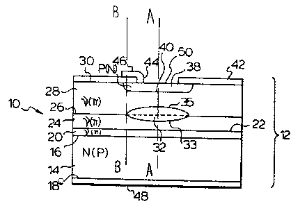
In FIGS. 1 and 2 the photodetector 10
includes a body of semiconductor material 12, a
substrate 14 having first and second major surfaces
16 and 18, respectively, and a buffer layer 20 having
a surface 22 which overlies the first major surface
16. A light absorptive layer 24 having a surface 26
overlies the surface 22 of the buffer layer 20. The
light absorptive layer absorbs light at the
wavelength of interest. An active layer 28 overlies
the surface 26 of the absorptive layer 24. The
active region 28 has a surface 30. A central zone 32
is located in the active region 28 and extends into
the absorptive region 24. The central zone 32 has a
first interface 33 extending into the absorptive
region 24 and a second interface 35 located within
the active region 28 spaced a distance from a cap
region 38. Cap region 38 extends a distance into the
active region 28 from the surface 30. The cap region
38 has a greater lateral extent, in the direction of
the plane of the surface 30, than the central zone
32. A PN junction 40 is formed at the interface
. . ~
1280~96
- 6 - Case 2997
between the active region 28 and the cap region 38.
A passivating layer 42 overlies the surface 30 and
has an opening 44 extending therethrough over the cap
region 38. A first electrical contact 46 overlies a
portion of the surface 30 exposed in the opening 44
to provide electrical contact to the cap region 38
and a second electrical contact 48 overlies the
second major surface 18. The first and second
electrical contacts 46 and 48, respectively, are a
means for providing an electrical contact to the
semiconductor body 12. Light incident on the
avalanche photodetector 10 typically enters the
semiconductor body 12 through the portion 50 of the
surface 30 exposed in the opening 44. In FIG. 2, the
photodetector has a contoured side wall 52.
The substrate 14 and the buffer, absorptive
and active regions 20, 24 and 28, respectively, are
of the same conductivity type and the cap region 36
is of the opposite conductivity type. Materials
comprising the buffer, absorptive, active and cap
regions are preferably chosen such that their lattice
constants are matched to that of the substrate to
within about 0.2 percent.
The substrate 14 is typically composed of a
semiconductor material such ~ N-type InP doped with
sulfur to a concentration of about 5 x 10¹³/cm3,
has sufficient thickness to support the remainder of
the structure. The substrate 14 is typically between
about 0.03 and 0.04 cm thick initially and has a
final thickness between about 0.01 and 0.015 cm
before dicing. The major surfaces 16 and 18 are
typically treated with Caro's acid or a one percent
bromine-in-methanol solution to remove surface
contamination and damage prior to the deposition of
the layers. The buffer region 20 is typically
.
1~30196
- 7 - Case 2997
composed of the same compound, is undoped and is
typically between about 4 to 6 micrometers ~um)
thick. The absorptive region 24 is typically
composed of a material which absorbs light at the
wavelength of interest in the range between about
1100 and 1700 nm. Suitable materials include
InO 53Gao 47As which absorbs at wavelengths less
than about 1650 nm and InxGal_xAsyPl_y which
absorbs light at wavelengths less than a maximum
wavelength determined by the choice of x and y as
disclosed, for example, by olsen et al in The Journal
of Electronic Materials 9, 977 (1980). ThiS layer is
preferably slightly ~-type conducting and is
typically deposited as undoped material containing
less than about 3 x 10¹⁵ donors/cm3 and
preferably from about 1 to 2 x 10¹⁵ donors/cm3.
The absorptive region 24 is preferably greater than
about 2 um thick and in the order of 6 ,um thick to
provide complete absorption of the incident light.
The active region 28 is typically composed of a
semiconductor material such as InP having an excess
conductivity modifier concentration less than about
3 x 10¹⁵/cm3 and is preferably between about .5
and 2 x 10¹⁵/cm3. The thickness of active region
28 between PN junction 40 and heterojunction 26 is
typically between about .5 to 1.5,um. The central
zone 32 typically has N-type conductivity and
contains an excess areal concentration of
conductivity modifiers above the background
concentration. This central zone is typically doped
with silicon which is embedded in the active region
28 50 that its center of concentration is spaced
either adjacent to or apart from the PN junction 40
and extends through the heterojunction 26 into the
absorptive region 24. The lateral extent of the
~801~6
- 8 - Case 2997
central zone 32 is less than that of the cap region
38. The cap region 38 is typically composed of a
light transmissive semiconductor material, such as
P-type InP, containing an excess of about 10 8
acceptors/cm3 and having a thickness between about
3 and 3.5 ~m. The first electrical contact 46 is
typically composed of a gold/zinc alloy deposited by
vacuum evaporation if the cap region is P-type and is
preferably configured so that light enters the
detector through that part of the cap region over the
central zone 32. The second electrical contact 48 is
typically composed of a gold/tin alloy deposited by
vacuum evaporation if the substrate 14 has N-type
conductivity. The passivating layer 42 is typically
composed of material such as SiO2,
borophosphosilicate glass or Si3N4 deposited
using evaporation, chemical vapor deposition, or
plasma-assisted deposition techniques.
The different regions of the semiconductor
body 12 may be sequentially formed on a substrate
surface using liquid phase or, preferably, vapor
phase epitaxy techniques such as those disclosed by
Olsen et al in U.S. Patent No. 4,116,733, issued
September 26, 1978 or by Olsen in GaInAsP Alloy
Semiconductors, T.P. Pearsall, Editor, John Wiley &
Sons (New York 1982), pages 11-41.
As shown in FIG. 3, the photodiode 10 is
formed by sequentially forming the buffer layer 20,
the light absorptive layer 24 and a first part 60 of
the active layer 28 which is typically between 0.1
and .3jum thick. Conductivity modifiers are then
embedded into a surface 62 of the first part 60,
preferably by ion implantation, into a central
portion 64 thereof to a depth of about O.l,um. As
shown in FIG. 4, a second part 68 of the active layer
~80196
- 9 - Case 2997
28 is then formed on the surface 62 to a thickness
between about 3 and 6,um. conductivity modifiers of
the opposite type are then embedded, typically by
diffusion techniques, into a surface 70 of the second
part 68 to form the cap region 38 over the central
portion 66. The excess conductivity modifier
concentration in the central portion 66 diffuses into
the second part 68 and absorptive region 24 during
subsequent high temperature processing steps.
To form the photodetector 10 of FIG. 2 the
cap region 38 is typicall~ deposited onto the surface
40 of the active region ~ and the contoured
sidewalls 52 are then formed using standard
photolithographic and etching techniques.
In the operation of the photodetector of
the invention a reverse bias voltage is applied
between the electrical contacts. The depletion
region along the line A-A of FIG. 1 increases with
increasing voltage, with the electric field reaching
a value of between about 2 and 4 x 10⁵ V/cm when
the active region 28 adjacent the PN junction 40 is
fully depleted. A further increase in the applied
voltage causes the depletion region to extend into
the absorptive region 24 where the electric field
increases and an electric field EM sufficient for
avalanche breakdown is reached at the PN junction
40. Assuming an abrupt PN junction, the peak
electric field EM along the line A-A of FIG. 1,
when the depletion region extends into the absorptive
region 24 is:
EM ~ (NAx + No + Nt WC)
whe~e q is the electronic charge, ~ is the dielectric
constant, NA is the conductivity modifier volume
concentration in the active region 28, x is the
thickness of the active region between the PN
1280196
- 10 - Case 2997
junction 40 and the surface 26 of the absorptive
region 24, No is the embedded areal conductivity
modifier concentration in the central zone 32, Nt
is the conductivity modifier volume concentration and
Wc is the thickness of the depletion region in the
absorptive region 24. No is typically between
about 1.5 and 3 x 10¹²/cm2 and preferably between
2 and 2.5 x 10¹²/cm~. The first two terms
represent the electric field necessary to deplete the
active region 28 including the central central zone
32. For example, if the electric field for avalanche
multiplication is approximately 4.5 x 10 V/cm then
the field to deplete the active region 28 is
preferably between about 2.5 and 3.0 x 10⁵ V/cm.
This electric field distribution is illustrated as a
solid curve, labelled A-A, in FIG. 5 where the
numbers on the abcissa correspond to the labels on
the surfaces of the photodetector 10 of FIG. 1. The
presence of the implanted central region 32
overlapping into the absorbing region 24 causes an
increase in the electric field in a narrow region of
the absorbing layer immediately adjacent to the
heterojunction 26.
The peripheral zone adjacent the central
zone 32 will also fully deplete with the application
of reverse-bias voltage. However, since the central
zone 32 is not present, the maximum electric field
(EM) along the lines B-B of FIG. 1 will be less
than that along the line A-A and also less than the
field required for avalanche multiplication. The
peak electric field Ep in the peripheral zone when
the depletion region extends into the absorptive
region 26 is:
Ep = -~- (NAx + Nt wp)
where wp is the thickness of the depletion region
: ' ' ` ' ~
1~80~96
- 11 - Case 2997
in the absorptive region 24 at the periphery. This
electric field distribution is illustrated as the
broken curve, labelled B-B, in FIG. 5.
FIG. 6 shows the impurity distribution for
the photodetector. From this diagram, it is evident
that the implant of silicon forming central zone 32
is diffused across the heterojunction 26 since the
lower interface 33 of the central zone 32 is shown
extending across the heterojunction 26. A distance
10 n d~ is shown in FIG. 6 between the center of the
implanted central zone 27 and the heterojunction 26.
This distance ~d~ is preferably within the range 0 to
.2 ~m. The silicon implant at 27 has a
quasi-guassian peak with a standard deviation of
approximately .2 ~m.
While not fully understood, it is believed
that the silicon implant 32 extending from the active
region 28 through the heterojunction, and the
resulting higher field at the heterojunction, may be
responsible for the observed fast response. This is
different from the effect of an intermediate
quaternary layer 25 (see FIGS. 7a and 7b) of InGaAsP
sandwiched between ~he active region 28 and the
absorptive layer 2~. It is known that the quaternary
layer minimizes slow response which occurs due to the
discontinuity in the valance band at the
heterojunction. The quaternary layer 25 would form
part of the overall absorptive region and the central
zone 32 would extend through the first heterojunction
into the quaternary layer, and for very thin
quaternary layers, also into the absorptive layer
24. It is believed that the combination of the
central zone 22 and quaternary layer 25 might lead to
faster response times. In FIG. 7a the central zone
32 extends through the neterojunction into the
.
.:
lX80~96
- 12 - Case 2997
quaternary layer 25. In FIG. 7b, the quaternary
layer is relatively thin and the central zone 32
extends through the quaternary layer 25 into
absorptive layer 24.