Note : Les descriptions sont présentées dans la langue officielle dans laquelle elles ont été soumises.
VECTOR CALCVLATION CIRCUIT CAPABLE
OF RAPIDLY CARRYING OUT VECTOR
CA~CULATION OF THREE INPUT VECTORS
This invention relates to a vector calculation
circuit capable of carrying out a vector calculation of
vectors. It is to be noted throughout the instant
5 specification that each of the vectors is composed of a
plurality of vector components or elements which are
given in the form of electrical signals and which are
electrically processed, although a specific description
will not be made hereinafter.
A recent requirement for an electronic digital
computer is to process a vector calculation at a high
speed. As such a vector calculation, a vector addition
is exemplified wherein a pair of vectors is added to
each other. In this event, the vector addition should
15 be repeated between ~he respective components of the
vectors a great number of times because each of the
vectors is composed of a lot of components.
~Z~314~
Furthermore, it often happens that the vector
addition must be carried out among three vectors each of
which is also composed of a great number of componentsO
In this case, two of the components are selected from
5 two of the three vectors and are added to each other by
the use of a vector adder to obtain a provisional sum.
Thereafter, one of the components is selected from the
remaining vector and is added to the provisional sum by
the above-mentioned vector adder to provide a primary
10 sum. Thus, the vector adder is used two times on
carrying out the vector addition of three vectors.
Likewise, it is frequently required in the
electronic digital computer to calculate a total sum of
a great deal of components of a single vector. In this
15 case, two of components are at first added to each other
by the vector adder to calculate a local sum.
Subsequently, the local sum is added to another
component by the vector adder. Similar addition is
successively repeated by the use of the vector adder to
20 calculate the total sum of the components.
~ t any rate, the vector adder should be
activated twice on carrying out the vector addition
among three components of the three vectors. This means
that the vector addition among three components is very
25 time-consuming.
L4~6
Summary of the Invention:
..... , ~
It is an object oE this invention to provide a
vector calculation circuit which can carry out a vector
addition among three vectors at a high speed.
It is another object of this invention to
provide a vector calculation circuit of the type
described, which can quickly calcula*e a total sum more
than two components.
It is still another object of this invention to
10 provide a vector calculation circuit of the type
described, which is convenient for processing a vector
or vectors composed of an enormous number of components.
According to an aspect of this invention, there
is provided a vector calculation circuit which is for
15 use in carrying out a vector calculation to provide a
result of said vector calculation in response to a first
vector composed of a plurality of first-set components
and a second vector composed of a plurality of
second-set components and selectively to a third vector
20 composed of a plurality of third-set components. The
vector calculation circuit comprises selecting means
responsive to one of the third-set components and a
fixed value of zero for selecting, as a selected
component, a selected one of the one of the third-set
25 components and the fixed value, a carry save adder
responsive to the selected component and requisite ones
of the first-set and the second-set components for
carrying out a carry save addition among the selected
~ ~314~
component and the requisite ones of the first-set and
the second-set components to produce a local sum and a
carry collectively as a result of the carry save
addition, an additional adder responsive to the local
5 sum and the carry for adding the carry to the local sum
to produce a primary sum of the local sum and the carry,
and means for producing the primary sum as the result of
vector calculation.
According to another aspect of this invention,
10 there is provided a vector calculation circuit which is
for use .in carrying out a vector calculation to provide
a result of said vector calculation in response to a
first vector composed of a plurality of first-set
components and a second vector composed of a plurality
15 of second-set components and selectively to a third
vector composed of a plurality of third-set componentsO
The vector calculation circuit comprises a carry save
adder responsive to the first, second, and third vectors
for carrying out a carry save addition of requisite ones
20 of the first- throuyh third-set components to produce a
local sum and a carry collectively as the carry save
addition, first selector means for selecting either of
the local sum and the requisite one of the first set
components as a first selected component, second
25 selector means for selecting either of the carry and the
requisite one of the second-set components as a second
selected component, an additional adder coupled to the
first and the second selector means for adding the first
26
selected component to the second selected component to
produce the result of the vector calculation.
Brief Description of the Drawings:
Fig. 1 is a block diagram of a conventional
5 vector calculation circuit for use in carrying out a
vector addition;
Fig. 2 is a time chart for use in describing
operation of the vector calculation circuit illustrated
in Fig. l;
Fig. 3 is another time chart for use in
describing another operation oE the vector calculation
circuit illustrated in Fig. l;
Fig. 4 is a block diagram of a vector
calculation circuit according to a first embodiment of
15 this invention;
Fig. 5 is a time chart for use in describing
operation of the vector calculation circuit illustrated
in Fig. 4;
Fig. 6 is a similar time chart for use in
20 describing another operation of the vector calculation
circuit illustrated in Fig. 4
Fig. 7 is another time chart for use in
describing a further operation of the vector calculation
circuit illustrated in Fig. 4;
Fig. 8 is a block diagram of a vector
calculation circuit according to a sécond embodiment of
this invention;
. :, ''
~v~ 6
Fig. 9 is a time chart for use in describing
operation of the vector calculation circuit illustrated
in Fig. 8,
Fig. 10 is a block diagram of a vector
5 calculation circuit according to a third embodiment of
this invention;
Fig. 11 is a time chart for use in describing
operation of the vector calculation circuit illustrated
in Fig. 10; and
Fig. 12 is anoth0r time chart for use in
describing another operation of the vector calculation
circuit illustrated in Fig. 10.
Descri tion of the Preferred Embodiments:
-- P ~
Referring to Fig. 1, a conv~ntional vector
15 calculati~n circuit will be descxibed at first for a
better understanding of this invention. The
conventional vector calculation circuit is for use in
carrying out a vector addition of a plurality of
vectors. In this connection, the illustrated vector
20 calculation circuit is specified by a vector adder 15
which is connected to first and second input lines 16
and 17. Two oE the vectors are supplied to the vector
adder 15 through the first and the second input lines 16
and 17, respectively, and may be called first and second
25 vectors A and B (such vectors being denoted herein by
ordinal letters rather than by thick letters).
It will be assumed that the first vector A is
composed of a sequence oE first-set components or
1~.gi~4~
element3 (al, a2, ..., an) which may be called first
through n-th co~ponents of the first vector A,
respectively. Likewise, the second vector B is composed
of a sequence of second-set components (bl, b2, ..., bn)
5 which may be referred to as first through n-th
components of the second vector B. Thus, the first
vector A is assumed to have the same number of
components as the second vector B in the illustrated
example.
The vector addition of the first and the second
vectors A and B is for calculating an output vector O
composed of a sequence of output components ~1~ 2'
' n) which may be called first through n-th output
components. Specifically, the vector adder 15
15 successively sums up the first-set and the second-set
P (al, a2, O-t an) and (bl, b2t ..., b ) to
produce the first through n-th output components (1
2' ' n) which appear on an output line 18.
Therefore, the output component i is collectively given
20 by:
i ai ~ bi '
where i is a variable between 1 and n, both inclusive.
It is to be noted here that the illustrated
vector adder 15 is also used for carrying out the vector
25 addition of three vectors which will be called first,
second, and third vectors A, B, and C composed of
first-set~ second-set, and third-set components ~a1, a2,
n ( 1' b2~ bn)r and (cl~ c2, ... , c ). In
4'~6
this event, the vector adder 15 successively sums up at
first the first-set components ai and the corresponding
second-set components bi to produce a local sum vector D
composed of local sum components di, where i is also a
5 variable between 1 and n, both inclusive~ The
above-mentioned s~mmation is therefore specified by:
di ai + bi.
The local sum components di are successively sent to the
output line 18.
Thereafter, the local sum components di are
successively added to the third-set components ci by the
vectox adder 15 to produce an output vector which is
depicted at O again and is composed of output components
(1~ 2~ n) appearing on the output line 18. As a
15 result, the output components i is collectively
represente~d by:
i = ai + bi + Ci-
In general, all of the local sum components dl
through dn are calculated by the vector adder 15 and are
20 thereafter added to the third-set components,
respectively. From this fact, it is readily understood
that the local sum components di should be held in a
register or registers Inot shown) and thereafter
supplied to the vector adder 11 again.
Practically, the vector adder 15 comprises a
plurality of flip-flops in addition to an adder so as to
carry out the vector addition in a pipeline fashion.
Each pair of the first-set and the second-set components
4~i
is successively delayed by the flip-flops .in response to
a sequence of clock pulses having a clock cycle and is
calculated to be produced through the output line 18 as
one of the output components after a predetermined
5 duration. Herein, it is possible to define the
predetermined duration as a calculation time for
calculating the vector addition of a single pair of the
components.
Referring to Fig. 2 together with Fig~ 1, the
10 first through third vectors A, B, and C are added to one
another by the use of the vector adder 15 illustrated in
Fig. l in a manner to be described later. In Fig. 2,
the calculation time is assumed to be equal to mT, where
m is an integer and T is representative of the clock
15 cycle mentioned above. In addition, the first
components al and bl of the first and the second vectors
and B are given to the vector adder 15 through the
first and the second input lines 16 and 17 in
synchronism with a ~eroth one of the clock pulses.
2~ Thereafter, the second through n-th components a2 and b2
through an and bn are successively given to the vector
adder 15 through the-first and the second input lines 16
and 17 in synchronism with first through (n ~ th ones
of the clock pulses, respectively. As a result, first
25 through n-th component pairs are arranged in first
through n-th time intervals or clock cycles,
respectively.
l4~
:LO
Responsive to the first components al and bl of
the first and the second vectors A and B, the vector
adder 15 produces a first one dl of the local sum
components of the local sum vector D through the output
5 line 18 in timed relation to an m-th one of the clock
pulses. As a result, the f.irst local sum component d
appears on the output line 18 in synchronism with the
m-th clock puls~ (m), as shown in Fig. 2. Likewise,
second through n-th ones d2 to dn of the local sum
10 components appear on the output line 18 in synchronism
with (m + l)-th through (n ~ m - l)-th ones of the clock
pulses, respectively. The first through n-th local sum
components dl to dn are sent to the registers to be sent
to the vector adder 15 again.
In Fig. 2, the third vector C and the local sum
vector D are given to the vector adder 15 through the
first and the second input lines 16 and 17. More
particularly, the first component cl of the third vector
C is supplied to the vector adder 15 simultaneously with
20 the first local sum component dl in synchron.ism with the
(n + m ~ th clock pulse. Similarly, the second
through n-th components c2 to cn of the third vector C
and the second through n-th local sum components d2 to
dn are supplied in pairs to the vector adder 15 in
25 synchronism with the (n ~ m)-th through (2n ~ m - l)-th
clock pulses.
As a result, a first output component l of the
output vector O appears on the output line 18 in
.synchronism with an (n ~ 2m - l)-th one of the clock
pulses. In a like manner, second through n-th output
components 2 to n are produced through the output line
18 in timed relation to (n + 2m)-th through
5 2(n + m ~ 1)-th clock pulses, respectively.
Accordingly, it takes a time duration of
2~n + m - l)T to carry out the vector addition of three
vectors, each of which is composed of n componerlts.
Let the vector adder 15 illustrated in Fig. 1 be
10 used for calculating a total sum of components. It is
presumed that the components are equal in number to 2n,
where n is a positive integer. In this case, the 2n
components are divided into first and second groups,
each of which is composed of 2n 1 components. The first
15 and the second groups of components may be recognized as
first and second vectors A and B, respectively. The
components of the first and the second vectors A and B
are collectively depicted at ai and bi and carry out the
vector addition of ai and bi in the above-mentioned
20 manner to produce local sum components ci, the number of
which is equal to 2n 1. Likewise, 2n 1 local sum
components ci are further divided into first and second
parts each of which is composed of 2n 2 local sum
components. The vector addition is carried out between
25 the local sum components ai' of the first part and those
bi' of the second part to produce 2n 2 additional sum
components ci'. Thereafter, similar procedures are
repeated by dividing such additional sum components into
~'~8~4~i
halv~s and by carrying out the vector addition between
divided components until calculation of the total sum
comes -to an end.
Let a calculation time between two components be
5 defined by mT like in the above-mentioned example when
the vector adder 15 is used to calculate the total sum
of the components equal in number to 2n.
Referring to Fig~ 3 in addition to Fig. 1, first
ones al and bl of the components of ~he first and the
10 second vectors A and B are given through the first and
the second input lines 16 and 17 to the vector adder 15
in timed relation to a zeroth one of the clock pulses.
Subsequently, second through 2n l-th components of the
first and the second vectors A and B are successively
15 supplied to the vector adder 15 in synchronism with
first through (2n 1 _ l)-th clock pulses, respectively.
In Fig. 3, a simplified symbol r is substituted for 2n 1
merely for simplification of illustration. The
simpli~ied symbol will be used also in the following.
First through r~th ones cl to cr of the local
sum components appear on the output line 18 in
synchronism with m-th through (r + m - l)-th clock
pulses, respectively, as shown in Fig. 3. Therefore, a
calculation time of (2n 1 + m - l)T is required to
25 calculate the 2n 1 local sum components. This shows
that it takes a first local calculation time of
(r + m - l)T to calculate a first local sum of the 2n 1
local sum components.
~'~8~426
:L3
Thereafter~ the first through r-th local sum
components cl to cr are divided into the first and the
second parts, each oE which is composed of 2n 2
components. A first pair al' and bl' of the components
5 of the ~irst and the second parts is supplied to the
vector adder 15 in synchronism with (r ~ m - l)-th clock
pulse. Subsequently, second through s-th pairs a2' and
b2' through as' and b~' are successively supplied to the
vectox adder 15 in response to tr ~ m ~ s - 2) clock
10 pulses, respectively, where s is equal to 2n 2 The
resultant additional sum components ci' appear in
response to (r + 2m - 1) through (r + s + 2m - 2) clock
pulses, where i is a variable between 1 and s, both
inclusive. Accordingly, a second local calculation time
15 for a second local sum of the 2n 2 local sum components
becomes equal to (2n 2 + (m - l))T.
In a like manner, local calculation times should
be added to one another to obtain a total calculation
time or calculating the total sum of 2n components.
20 Therefore, the ~otal calculation time is given by:
n-l . n-l . n-l
~ (21 ~ m - l)T = { ~ 21 + ~ (m - l)~T
i=O i=O i=O J
= {2n ~ n(m - l)}T.
In order to reduce 2n components into 2k
components by carrying out the addition in the
above-mentioned manner, where k is a positive integer
smaller than n, a partial calculation time is given by:
~ 64768-167
n-l n-l n-]
~ (21 + m - l)T = ~ ~ 21 ~ ~ (m ~ T
i=k ~i=k i=k
= ~2n _ 2k ~ (n - X) (m - 1)~ T-
If n, m, and k are equal to ~, 3, and 2, respectively, the
total calculation time and the partial calculation time are equal
to 23T and 16T, respectively.
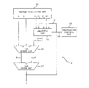
Referring to Figure 4, a vector calculation circuit 21 accord-
ing to a first embodiment oE this invention is for use in combin-
ation with a vector production circuit 22 and a calculation con-
trol circuit 23, both of which are operable in a manner to be
described later.
The vector production circuit 22 may be, for example, vector
registers while the calculation control circuit 23 may be, for
example, a timing controller operable in a manner to be described
in conjunction with Figure 5.
The vector calculation circuit 21 is supplied from the vec-
tor production circuit 22 with first and second vectors A and B
together with first through L-th additional vectors C1 to CL,
where L is a positive integer. Furthermore, a fixed value of "0"
(zero) is also supplied from the vector production circui-t 22 to
the vector calculation circuit 21.
It is surmised that each of the first and the second vectors
A and B and the first through L-th additional vectors Cl to CL is
composed of first through n-th components, where n is also a pos-
itive integer. In this connection, the first through n-th com-
ponents of the first and the second vectors A and B are represent-
ed by tal, a2, ... r an) and (bl, b~, ..., bn), respectively.
~1~8~a~f~6
14a 64768-167
Likewise, the first through n-th components of the first through
L-th additional vectors
314'~
Cl to CL are collectively represented by (cjl, cj2, ....
cjn), where j is a variable between 1 and L, both
inclusive.
The first through L-th vectors Cl to CL are
5 given to a selector circuit 25 which is supplied from
the calculation control circuit 23 with a control signal
CT and which is controlled in response to the control
signal CT, as will become clear as the description
proceeds. The selector circuit 25 is also given an
10 internal vector V which is composed of first through
n-th components vl to vn and which will be described
later.
Under the circumstances, the first components of
the first through L-th additional vectors Cl to CL and
15 the internal vector V are supplied to the selector
circuit 2S as a first component set together with the
fixed value of ~ero at a first time instant. Likewise,
the second through n-th components of the respective
vectors Cl to CL and are produced as second through n-th
20 component sets at second through n-th time intervals,
respectively~ Accordingly, an i-th component set
produced at an i-th time interval is collectively
represented by cji, vi, and 0, where i is a variable
between 1 and n, both inclusive.
Responsive to the control signal CT, the
selector circuit 25 selects one o~ cji, vi, and 0 as a
selected component di at an i-th time interval.
Inasmuch as such selection is successively carried out
4q~
16
at the first through n-th time intervals, the selector
circuit 25 produces a third vector D composed of Pirst
through n th components dl to dn which may be called
third-set components. ~t any rate, one of the third-set
5 components dl to dn is produced as a selected component
from the selector circuit 25.
A first adder circuit 26 is operable in response
to the first, the second, and the third vectors A, B,
and D and comprises a carry save adder for carrying out
10 a carry save addition of the first through third vectors
A, B, and D. In addition, the first adder circuit 26
may comprise a plurality of flip-flops like in the
vector adder 15 (Fig. 1) so as to process the first
through third vectors A, B, and D in a pipeline fashion.
More specifically, the first adder circuit 26 is
given the first components al, bl, and dl of the first
through third vectors A, s, and D in parallel at the
first time interval. The second through n-th components
of the first through third vectors A, B, and D are given
20 to the first adder circuit 26 at the second through n-th
time intervals in a similar manner in parallel. In this
event, the i-th component di of the third vector D is
given from the selector circuit 25 as the selected
component while the remaining i-th components ai and bi
25 of the first and the second vectors A and s are given
~rom the vector production circuit 22 as requisite
components of the first and the second vectors A and B.
17 ~'~8~4~ 6~768-167
Under the clrcumstances, the first adder circuit produces
a result of the carry save addition of three parallel components
when a predetermined calculation time of mT lapses after recep-
tion of the three parallel components, where T is representative
of a clock cycle of clock pulses, like in Figure 1.
It is mentioned here that the first through i-th time inter-
vals are defined by zeroth through (i - l)-th clock pulses, re-
spectively, like in Fiyures 2 and 3.
The result of the carry save addition which appears at the
i-th time instant is divisible into a local sum ei and a carry fi.
Herein, a sum of the local sum ei and the carry fi is equal
to a sum of the three components ai, bi, and di, and is therefore
given by:
ei + fi = ai + bi + di- (1)
More particularly, when each of the components ai, bi, and
di is represented by z bits, each bit ei(q) of the local sum ei
and each bit fi(q+l) of the carry fi are defined by:
ei(q) = ai(q) ~3 bi(q) ~ di(q)
i(q 1) ai(q)bi(q) + bi(q)di(q) + di(q)ai(q)~ (2)
where an encircled plus sign is representative of an addition
modulo 2 and q is a variable between 0 and z, both e~clusive.
As a result~ a succession oF the local sums and a succession of
the carries may be recognized as first and second result vectors
E and F, respectively, when the local sums and the carries are
successively produced from the first time interval to the n-th
time interval. The first and the second result vectors E and F
are therefore represented by:
L4;26
18
E = (el, e2, .~., en) and
F = (fl~ f2' ' fn)-
A second adder circuit 27 is connected to the
first adder circuit 26 in cascade to add the first
5 result vector E to the second result vector F to produce
a primary vector G which is composed of first through
n-th primary sums (glr g2' ~ gnj. From this fact, it
is readily understood that the i-th primary sum gi is
given by:
gi ei ~ fi.
The primary sum gi is finally produced as a
result of the vector calculation on one hand and i5 fed
back to the selector circuit 25 as the component vi of
the internal vector V.
It is to be noted here that such a cascade
connection of the first and the second adder circuits 26
and 27 requires no extra clock pulse and never prolongs
the calculation time.
Referring to Fig. 5 together with Fig. 4 r let
20 the vector addition be carried out among the first and
the second vectors A and B and the second additional
vector C2. In this case, it is supposed that each
vector A, s, and C2 is composed of n components and that
each calculation time for the three parallel components
25 is defined by mT, as mentioned before. In this case,
the first and the second vectors A and B are composed of
tal, a2, ..., a ~ and tbl, b2, ..., bn) r respectively,
.
19 ~ 2~
while the second additional vector C2 is composed of
(C21~ C22~ C2n)
At first, the selector circu.it 25 successively
selects the first through n~th components tc2l, c22,
S ..., c2n) of the second additional vector C2 in r~sponse
to the control signal CT. The resultant components
(C21' C22' - ~ c2n~ are delivered from the selector
circuit 25 to the first adder circuit 26 as the first
through n-th components tdl, d2, ..., dn~ of the third
10 vector D, respectively. On the other hand, the first
adder circuit 26 is given the first through n-th
components al to an and bl to bn of the first and the
second vectors A and B in pairs.
In Fig. 5, the first components a1, bl, and c2l
15 of the respective vectors A, B, and C2 are synchronized
with the zeroth clock pulse while the second components
a2, b2, and c22 are synchronized with the first clock
pulse. The first components a1, bl and c21 are added to
one another through the first and the second adder
20 circuits 26 and 27 and are produced as the first primary
sum g1 in synchronism with the m-th clock pulse.
Likewise, the second components a2, b2, and c22 through
n-th components an, bn, and c2n are successively added
to one another to be produced as the second through n-th
25 primary sums in synchronism with the (m ~ th through
(n ~ m - 1) th clock pulses~ as illustrated in Fig. 5.
This shows that a total calculation time becomes
equal to (n ~ m - l)T so as to carry out the vector
.4~2~
calculation of three vectors each of which is composed
of n components. If n and m are equal to 4 and 3, the
total calculation time can be represented by 6T and is
considerably shortened in comparison with the
5 conventional total calculation time of 12T described in
conjunction with Fig. 2.
Referring to Fig. 6 in addition to Fig. 4,
description will be made about calculating a total sum
of 2n components. The components are divided into first
10 and second groups which may be recognized as first and
second vectors A and Bo The first and second vectors A
and B are composed of first through 2n l-th (namely,
r-th) components (al, a2, ..., ar) 1 2
br), respectively, where r is equal to 2n 1. It is
15 assumed like in Figs~ 1 through 3 that the calculation
time of mT is taken 50 as to carry out the vector
addition of each set of the components of three vectors.
Under the circumstances, no primary sum appears
from the second adder circuit 27 before production of
20 the m-th clock pulse. Therefore, each pair of the first
through mwth components of the first and the second
vectors A and B may be successively added by the first
and the second adder circuits 26 and 27 in synchronism
with the zeroth through (m ~ th clock pulses. Taking
25 this into consideration, the selector circuit 26 selects
the fixed value of zero as the components of the third
vector D before production of the m-th clock pulse.
As a result, the first adder circuit 26
successively carries out the vector addition of the
components ai and bi with the component di kept at "0"
to produce the local sum ei and the carry fi which are
5 defined by E~uation (1~. The local sum ei and the carry
fi are summed up by the second adder circuit 27 to
produce the primary sum gi representativa of the result
of vector addition of ai, bi, and 0.
After lapse of the calculation time of mT, the
y gl, g2, .. are added to the selactor
circuit 25 as the component vi of the internal vector V.
As-a result, the first primary sum gl appears in
synchronism with the m-th clock pulse, as illustrated in
Fig. 6. At any rate, the primary sums gl, g2, ... are
15 successively selected as the (m + l)-th, (m ~ 2)-th, ...
components of the third vector D by the selector circuit
25 after production of the m-th clock pulse.
Consequently, the illustrated vector calculation circuit
21 can carry out the vectox calculation of the three
20 vectors A, Bt and D after the m-th clock pulse is
produced. This shows that the (m + l)-th through
2n l-th component pairs of the first and the second
vectors A and B are added to the (m ~ l)-th through
2n l-th components dm~l to dr of the third vector D
25 after reception of the m-th clock pulse. When the
(m -~ l)-th through 2n l-th components are collectively
depicted at an i-th component, the primary sums may be
collectively represented by gi m
22 ~ 42~
Thus, the first adder circuit 26 carries out the
carry save addition of ai, bi, and di to successively
produce the local sum ei and the carry fi as regards the
(m + l)-th through 2n l-th components of the first and
5 the second vectors A and ~.
The second adder circuit 27 successively adds
the local sum ei and the carr~ ~i to produce the primary
sum gi which is sen t to the selector circuit 25 as the
component vi_m of the internal vector V.
Let the primary sums be counted from the m-th
clock pulse and be represented by gi. Among the output
components gi, only partial ones of the primary sums,
Y~ gl~ g2~ gr-m are sent to the selector
circuit 25 while the remaining primary sums gr m~l
15 through gr appear as results of vector calculations.
As shown in Fig. 6, it takes a first local
calculation time of t2n 1 + m - l)T to obtain the
remaining primary sums, m in number.
The remaining primary sums gr_mfl to g~ are
20 equal in number to m and are given by:
gr-m+l ar-m+l + ar-2m~1 + ar-3m+1 + '
+ br m+l * br-2m-~1 + br-3m+1 -
gr-m*2 = ar-m+2 ~ ar-2m+2 + ar-3m~2 -
+ br-m~2 + br-2m+2 ~ br-3m+2
gr r ar-m + ar-2m + --
+ br + br-m ~~ br-2m
23 ~Z~4'~6
Accordingly, it is possible to calculate the
total sum of the 2n components by totalizing the
above-mentioned primary sums equal in number to m.
Herein, consideration is made about a second
5 local calculation time for totaliziny the primary sums,
m in number. At first, a certain positive number k is
selected such that m be smaller than 2k and greater than
2 l, namely:
2k ~ m > 2k~1
lO In this case, the second local calculation time can be
represented by:
{2 - l ~ k(m - l~}T.
A total calculation time for the total sum is
equal to a sum of the first and the second local
15 calculation times and is therefore given by:
(2n l ~ m - l~T ~ {2k _ l + k(m - l)T}
= {2n l + 2k _ l + (k + l)(m - l)}T.
If n, m, and k are equal to 4, 3, and 2,
respectively, the total calculation time becomes equal
20 to 17T.
Referring to Fig. 7, another calculation is
carried out by the use of the vector calculation circuit
21 illustrated in Fig. 4 so as to calculate a total sum
of the first and the second vectors A and B each of
25 which is composed of components, 2n l in number. In
Fig. 7, first through m-th primary sums are calculated
in the above-mentioned manner as regards first through
p-th ones of the components, where p = 2n 1 _ t and
24
where, in turn, t represen~s a positive integer. As
regards the remaining components f t in number, the
vector addition of two vectors is carried out after
production of a p-th clock pulse, as shown in Fig. 7.
5 As a result, primary sums, (m + r) in number, are
readily calculated and can be represented by gp m~l~
gp-m+2' ' gp' ~ gr- Therefore, it is possible to
select the nu~ber of the primary sums at a pxedetermined
number which is not smallex than m.
Referring to Fig. 8, a vector calculation
circuit 21' according to a second Pmbodiment of this
invention is supplied from a vector production circuit
(not shown in Fig. 8) with first, second, and third
vectors A, B, and C which are composed of first through
15 n-th components (al, a2, -~ anJ~ ( 1 2 n
and tc1, c2, ..., cn), respectively. The first through
third vectors A to C are given to a first adder circuit
26 which is similar in structure and operation to that
illustrated in Fig. 4 while the first and the second
20 vectors A and B are given to first and second selectors
31 and 32.
The first adder circuit 26 carries out a vector
addition of the first through third vectors A to C in
the manner illustrated in Fig. 4 to produce a result of
25 carry save addition whlch is divisible into first and
second local vectors D and E. The first and the second
local vectors D and E are composed of first through n~th
local components (dl, d2, Ø, dn) and (el, e2, -~ en)
~ 25 1'~4~G 64768-167
which represent local sums and carries appearing on the carry
save addition, respectively. Like in Equations (1) and (2), the
local swm and the carry can be collectively given by:
di + ei = ai + bi + Ci'
di(q) ai(q) ~ bi(q) ~ ci(q), and
i(q) ai(q)bi(q) + bitq)Ci(q) ~ Ci(q)ai(q)~ (3)
where i is variable between 1 and n, both inclusive and q is a
variable between 0 and z when each components ai, bi, and ci is
composed of z bits.
The first and the second local vectors D and E are delivered
to the first and the second selectors 31 and 32 which are supplied
with the first and the second vectors A and s, respectively. The
first and the second selectors 31 and 32 are operable in response
to a control signal (not shown) given from a calculation control
circuit (not shown in Figure 8).
Consequently, the first selector 31 selects either the com-
ponent ai of the first vector A or the component di of the first
additional vector D to produce a first selected component fi
which forms a first selected vector F. ThiS shows that the first
selected vector F is composed of (fl~ f2, ~ fn) Likewise,
the second selector 32 selects either the component bi of the
second vector B or the component ei of the second additional
vector E to produce a second selected component gi which forms
a second selected vector G composed of (gl~ g2~ ~ gn)
The first and the second selected vectors F and G are sent
to a second adder circuit 27 which is similarO
L4~6
26
in structure and opera~ion to that illustrated in Fig.
4. The second adder circuit 27 adds the first selected
component fi to the second selected component gi to
produce an output vector H composed of first through
5 n-th output components (hl, h2, ..., hn). In this
event, the i-th output component hi is given by:
hi = fi ~ gi.
Referring to Fig. 9 afresh and Fig. 8 again, it
is assumed that the first through third vectors have
10 first through n-th components (al, a2, ..., an), (bl,
2 n (cl, c2, ..., cn) and are added to one
another by the use of the vector calculation circuit 21'
illustrated in Fig. 8~ It is also assumed that first
through n-th sets of three components (al, bl, cl), (a2,
15 b2, c2), ..., (an, bn, cn) are successively given to the
vector calculation circui~ 21' and that a calculation
time for each set is equal to mT, where m is a positive
integer and T is a clock cycle.
Each set of the three components is ~ollectively
20 depicted at ai, bi, and ci and is added by the first
addPr circuit 26 into the first and the second local
components di and ei.
On the vector addi~ion of ~hree vectors, the
first and the second selectors 31 and 32 select the
25 first and the second additional vectors D and E,
respectively, in response to the control signal.
Therefore, the first local components di and ei are
selected by the first and the second selectors 31 and 32
~X~14~6
27
to be produced as the first and the second selected
components fi and gi, respectively. Thereafter, the
first and the second selected components fi and gi are
added by the second adder circuit 27 to produce the
5 output component hi.
As shown in Fig. 9, the first set of the
components al, bl, and c1 are given to the vector
calculation circuit 21' in synchronism with the zeroth
clock pulse while the output component hl is produced in
10 synchronism with the m-th clock pulse. The output
component hn which results from the n-th set of an, bn,
and cn is produced in synchronism with an (n + m - l)-th
clock pulse. Accordingly, the vector addition of three
vectors can be completed in a calculation time of
15 tn + m - 7)T.
Referring to Figs. 10 and 11, a vector
calculation circuit 21" according to a third embodiment
of this invention is similar in structure and operation
to that illustrated in Fig. 8 except that the output
20 vector H is supplied to the first adder circuit 26 as
the third vector ~ This structure is helpful for
calculating a total sum of components equal in number to
2n like in Fig. 4. The components, 2n in number, are
divided into first and second vectors A and B which are
25 composed of first through 2n l-th (namely, r-th)
components tal, a2, ..., ar) and (bl, b2, ~ b ),
where r is equal to 2n 1 As shown in Fig. 11, the
first through r-th components are succes~ively given to
8142~
28
the vector calculation circuit 21" in pairs in timed
relation to zeroth through (r - l)-th clock pulses,
respectively. Let the i-th components ai and bi be
added to each other by the vector calculation circuit
5 21" where i is variable between 1 and 2n 1, both
inclusive, and be calculated for a calculation time of
mT like in Figs. 4 and 8.
Like in Fig. 4, the output components can be
used as the components of the third vector C after
10 reception of the m-th clock pulse. Taking the above
into account, the illustrated vector calculation circuit
~1" carries out the vector addition of the irst and the
second vectors A and B when the first through m-th
components ara given to the vector calculation circuit
15 21". The vector addition of the first through third
vectors A, B, and C is carried out in the vector
calculation circuit 21" when the m-th clock pulse is
produced. For convenience of description, the output
components hl through hr are given to the first adder
20 circuit 26 as (m + l)-th through (m + r)-th components
Cm~l to cm+r, reSpectively.
More particularly, when i is not greater than
(m + 1~, the first and the second selectors 31 and 32
select the components ai and bi of the first and the
25 second vectors A and B, respectively. Therefore, the
components ai of the irst vector A are successively
sent from the Pirst selector 31 as the first selected
components fi while the components bi of the second
3~;~8~4~6
29
vector B are successively sent from the second selector
32 as the second selected components gi, where i = 1, 2,
--, m.
The first and the second selected components fi
5 and gi are added to each other by the second adder
cixcuit 27 to be produced as the output components hi
which successively appear after lapse of the calculation
time mT, as shown in Fig. 11. In this connection, it is
readily understood that the second adder circuit 27
10 comprises a plurality of flip-flop stages, m in number,
in addition to an adder.
When i is greater than m, namely, i = m
m + 2, ..., 2n 1, the output components hi m are
successively sent back to the first adder circuit 26 as
15 the i-th components of the third vector C. The first
adder circuit 26 successively carries out the carry save
addition of three components, namely, ai, bi, and ci in
response to the m-th through (r ~ th clock pulses to
produce the first and the second local components di and
20 ei which are given by Equation (3) and which are given
to the first and the second selectors 31 and 32,
respectively.
After lapse of the calculation time mT, the
first and the second selectors 31 and 32 select the
25 first and the second local components di and ei as the
first and the second selected components fi and gi,
respectively. The first and the second selected
components fi and gi are successively added to each
.426
other by the second adder circuit 27 in the
above-mentioned manner to produce the output component
hi-m.
From this fact, it is readily understood that
5 the output components hi m are sent back to the first
adder circuit 26 as the components ci of the third
vectox C for a duration defined be~ween the m-th clock
pulse and the 2n l-th (namely, r-th) clock puls~.
Counted from the m-th clock pulse, the output components
10 may be represented by hi and are given as the components
ci+m of the third vector C. Among the output components
hi, only partial ones of the output components, namely,
hl, h2, ..., hr m are sent to the first adder circuit 26
while the remaining cutput components hr m+l through hr
15 appear as results of vector calculations.
The remaining output components hr m+l through
hr are given by:
r-m+l ar-m+l + ar-2m~1 ~ ar-3m~1 +
+ br-m+l ~ br-2m~ br-3m+1
hr-m+2 ~ ar-m+2 ~ ar-2m+2 + ar-3m+2 + --
~ br~m+2 + br-2m+2 + br-3m+2
25hr = ar + ar-m ~ ar-2m
+ br ~ br-m ~~ br 2m +
As mentioned above, the results of vector
calculations are equal in number to m and must be
.426
31
further summed up so as to calculate the total sum of 2n
components.
In order to sum up the results, m in number, let
a positive number j be selected such that j satisfies
5 the following condition:
2i ~ m ~ 2i 1.
Taking the positive number j into account, a
time for the summation of the m results is given by:
~ (m - l)}T.
Therefore, a total time is given by summing up
the first and the second summation times and is
therefore defined by:
(2n 1 + m - l)T + {2j - 1 + j(m - l)}T
= ~2n 1 + 2j - 1 + (j + l)(m - l)}T.
When n and m are equal to 4 and 3, respectively,
the total time becomes equal to 17T because j = 2.
Referring to Fig. 12, another calculation may be
carried out by the vector calculation circuit 21"
tFig. 10) in a manner different from that illustrated in
20 Fig. 11. As shown in Fig. 12J the components! 2 in
number, of each vector ~ and B are divided into first
and second parts which are composed of p and t
components, respectively, where p is equal to
(2n-1 t)
As regards the first part of p components,
addition is successively carried out in consideration of
the output vector ~ in the above-mentioned manner. As a
result, calculation results, m in number, are calculated
4~6
32
after the p-th clock pulse and appear as hp m~l~ hp m+2
..., hp.
On the other hand, the first and the second
vectors A and s are added without the third vector C as
5 regards t components of the first and the second vectors
A and B to produce calculation results, t in number,
which appear as hp~l, hp~2, ..~, hr, where r is equal to
2n-1
The calculation results, (m ~ t) in numberr are
10 further added to one another in a manner similar to that
illustrated in Fig. 11 to calculate the total sum of 2n
components.
While this invention has thus far been described
in conjunction with a few embodiments thereof, it will
15 readily be possible for those skilled in the art to put
this invention into practice in various other manners.
For example, the first adder circuit 26 illustrated in
Figs. 8 and 10 may be connec~ed to a selector circuit 25
as shown in Fig. 4 so as to select one of vectors given
20 to the first adder circuit 26. At any rate~ the vector
calculation circuit illustrated in Figs. 8 and 10 can
respond to a plurality of vectors which are greater in
number than three.