Note : Les descriptions sont présentées dans la langue officielle dans laquelle elles ont été soumises.
~33L77
BIAS CIRCUIT FOR FET
BACKGROUND OF THE INVENTION
The present invention relates to a bias circuit for
a transistor and, more particularly, to a bias circuit
which ~s provided means for compensating for deviations
in the threshold voltage of a field effect transistor
(FET).
A prior art bias circuit for an FET comprlses a
voltage dividing resistor which applies a gate bias to
the FET. The problem with this type of bias circuit is
10 ~ that the,voltage dividing resistor does not compensate- - -
: for scattering of the threshold voltage VT of the FET... ..
-,~: ..,,,,,~, ,~,,..Another prior art bias circuit-.for-F-ET is:~disclosed -
.... .:... , in the paper entitled-"Broadband GaAs-Monolithic Amplifier" ----
and presented by Onoda et al at the 1984 National Meeting
of the Institute of Électronics and Communication Engineers
,, ,,~,,,,,: of,Japan,,April 1984.,..The bias circuit proposed:,:by -.--:- :-:--:-
Onoda et al is constructed to shift the operating point
of an FET by a negative feedback circuit so that
~scattering of the threshold value VT may be compensated
for. However, the compensation attainable with such a
bias circuit is not satisfactory.
~2~33~7~
SUM~IARY OF THE INVENTION
It is therefore an object of the present invention
to provide a new bias circuit which confin~;errors in
operating current to a narrow range over a wide range
of threshold voltages VT and is feasible for installation
in an integrated circuit.
In accordance with the present invention, there is
provided a bias circuit having a resistor connected between
two power supply terminals and supplying a voltage appearing
at a first division point of the reisstor to a first FET
as a gate bias, comprising: a second division point which
lS provided on the resistor; and a second FET having a
drain'or a source thereof connected to the second division
,
- point, a gate voltage of the second FET being connected to
~, , . , :
-15--- a~predetermined.;potential-point.~
BRIEF DESCRIPTION OF THE DRAWINGS
The above and other objects, features and advantages
of the present invention will become more apparent from ,,,
~the following detailed description taken with the .
accompanying drawings in which:
Figs. 1 to 4 are schematic diagrams respectively
showing a first to a fourth embodiments of a bias circuit
for an FET in accordance with the present invention;
Figs. 5 and 6 are graphs showing characteristics of
~a bias circuit of the present invention together with those
of a prior art circuit which is shown in Fig. 7; and
. .
~ ,:
~33~L77
Fig. 7 is a schematic diagram of the prior art bias
circuit for an FET.
DESCRIPTION OF THE INVENTION
To better understand the present invention, a brief
reference will be made to a prior art bias circuit for
an FET, shown in Fig. 7. As shown, a resistor 53 which is
connected to power supply terminals 54 and 55 supplies a
bias voltage to a gate of an FET 51 via a resistor 52.
As previously stated, this kind of arrangement is
disadvantageous in that because the bias voltage, or
voltage divided by the resistor 53, is constant, any
'' deviation in the threshold voltage VT of the FET re'sults
in a deviation in the operatlng polnt of the FET.~ In
.. . . ............. ......
,,,.,..,, ~,~ : Fig.:.7,"the referen,c~e.numerals 56-and 57-respectively~--~' - :~ ---.--
.__r,.-,. ..,,~.,_,.~",,15..,,~designate.,-power,.supply--~erminals-~-for-,~the- E'ET 51-.
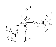
Referring to Fig.- l, a--first embodiment of~the bias ~
circuit in accordance with the present invention is shown.
,~. ., j ,An FET 12 is shown as having-a drain-and a source:~connected
, 'to power supply terminals 9 and 10, respectively, and a
gate connected to one end of a resistor 11. Those elements
which are designated by the reference numerals 1 to 8
constitute.the bias circuit which biases the FE~T 12.
Specifically, a resistor 1 which is connected to power
supply terminals 4 and 5 is divided at a point of division
2 so that a gate bias is applied to the FET 12 via the
~'~83~L~7
resistor 11. So far as such a system is concerned, this
embodiment is the same as the prior art.bias circuit of
Fig. 7. A characteristic feature of this particular
embodiment is an FET 8 which has a drain connected to
S another point of division 3 of the resistor 1, and a gate
and a source connected to power supply terminals 6 and 7,
respectively. It is important to note that the FET'8 is
different in size from the FET 12 but fabricated at the
same process step as the FET 12 and is equal in threshold
voltage VT to the FET 12.
The division points 2 and 3 of the resistor 1 may
have any of three dif~erent relative positions, i.e., a
.. ., : . . . .
' position of Fig. l wherein the division point 2 has a
' ' higher potential than the divlsion polnt 3, a positlon of
.. ~ 15 Fig. 2 wherein,the,.division-:points 2 and 3--have--the-~same
,potential, and.a_.position.of-Fig..3--wherein-the-~di-vision~
., . point 3 has a higher potential than the division point 2.
The division point 2 is determined by potentials at the-
power supply terminals 4, 5 and 10 and a predetermined --.-
: 20 voltagë across the gate and source of the FET 12.
~owever, the division point 3 is open to choice so long
as it remains higher in potential than the power supply
terminal 7 and ensures a voltage across the drain and
source of the FET 8. These are the reasons which account
for the threé alternatlve connections as shown in Figs.
.1 to 3. Because all of the three connections share the
~Z8~ 7
same operation principle, the following descxiption will
concentrate on the connection of Fig. 1 by way of example.
In Fig. 1, the voltage across the power supply
terminals 6 and 7 is so set up to have a threshold value
VTl. Assuming that the designed threshold voltage of the
FETs 8 and 12 is VT0~ the following relationship is set up:
VTl < VT0 < 0
When the threshold value VT of an actually manufactured
FET is greater than the threshold value VTl, the FET 8
remains turned off so that the voltage at the terminal 2
is equal to the divided voltage. As the threshold value
VT becomes'equal to or smaller than the threshold value VTl,
- - -` the FET 8 is turned on to cause a current to flow with the
. _ ,result:~that the voltage.at~,.,the.:terminal--3--is-:lowered-;due-to~
15 _,~the..resultant voltage,drop,..~,This.-,lowers:--the-voltage at-the=~
terminal (division point) 2 which is applied to the gate'
of the FET 12. Further, when the threshold value VT is
, equal to or smaller than the threshold value VTl and the
--latter is ~smaller than the threshold value VTo, the FET.
current IDS becomes greater than in the case with the
threshold value VTo. But, the voltage at the terminal
., ~ ' (dlvision point) 2 is lowered to shift the currenk IDS to. -
a lower sLde. Therefore, the d0gree of deviation of the
current can be reduced, compared to the prior art system
of Fig. 7.
3~77
By adequately selecting the size of the FET 8, it is
possible to provide a bias circuit which compensates
for scattering of the threshold voltage VT, as represented
by a graph of Fig. 5. In Fig. 5, the abscissa is indicative
of threshold voltages VT of the FETs 8 and 12 and the
ordinate, the drain source current IDS of the FET 12.
As~uming that the allowable range of current values"is
~20 percent, while the range of threshold voltages VT
attainable with the prior art circuit of Fig. 7 is limited
to VL < VT < VH as represented by a characteristic ~ ,
that of the present invention is as wide as VL' < VT ~,V~
as represented by a characteristic ~ . Further, in the
circuit of Fig. 1 if VTl is greater than VTo and the
division point 2 is'selected to bé higher~in potential
;15 than that of-Flg.,-7,jthe maximum-value-,can--be shifted-to -~
. . ~ . ~ . . . ..................... . . . . .
,~ ~ ,~ ,the vicinity_o~_VT_,-~VT0 as represented--by-a-characteristic-
~~ of Fig. 6, so that a bias circuit which compensates
for the threshold voltage scattering in both the cases of
.......
`'', , -~, VT'< VTo and VT > VTQ is achievable.' That is, the allowable
. :-20 range of VT deviation is extended from Al to A2, as shown
Fiy. 6.
Referring to Fig. 4, a more specific embodiment of
the present invention is shown. The bias circuit of Fiy. 4
is applicable to an FET whose threshold voltaye VT is
25' nearly equal to -1 volt. As shown, the bias circuit
includes a positive power supply terminal 4, a neyative
.
7 --
power supply terminal 5 and a ground terminal E. The
bias circuit is constructed such that when the threshold
voltage VT of the FET 12 has been lowered beyond the order
of -7 volt, a diode 13 turns on the FET 8. The operation
principle of this embodiment is the same as that of Fig. l.
In summary, it will be seen that in accordance with
the present invention an extra FET adapted to compen'sate
for variations of threshold voltage VT is added to an
ordinary resistance-division type bias circuit, so that
errors of operating current of an FET are confined in a
narrow range over a wide range of threshold values VT.
In addition, the bias circuit of the present invention
!' , ' -" ~' '~ " " can be fabri'cated~at the same process step as an FET and
'a resi'stor and,'hence,'~it 'is optimum not only~as a blas~
15 ' ;circuit of a slngle FET but aiso as a~ias circuit which~
,. . , - . , , .. , . ... - - . ,.,,, ,. , - .. . , . . ~ . . . ..... .. . . .
_ is to be built in an_integrated.:circuit chip.-~
. .
\ ' , ' , , .