Note : Les descriptions sont présentées dans la langue officielle dans laquelle elles ont été soumises.
0334L
CHANNEL ELECTRON MULTIPLIER
Backqround of the Invention
This invention relates to a channel electron
multiplier made from a monolithic ceramic body and a
method of making same. In particular it relates to a
channel electron multiplier wherein said channel
provides a preferably three dimensional, curved
conduit for increased electron/wall collisions and
for a device of smaller dimension, particularly when
longer channel length is required.
In one of its embodiments, this invention
provides for an electron multiplier device comprising:
a monolithic electrical insulating ceramic
body, at least one entrance port in said body and at
least one exit port in said body, and at least one
hollow curved passageway through said body extending
between each pair of entrance and exit ports, wherein
the walls of said hollow passageways include secondary-
emissive dynode material, and wherein the walls of said
passageway are non parallel with respect to the lateral
surface of said body.
Electron multipliers are typically employed
in multiplier phototubes where they serve as
amplifiers of the current emitted from a photocathode
when impinged upon by a light signal. In such a
multiplier phototube device the photocathode,
electron multiplier and other functional elements are
enclosed in a vacuum envelope. The vacuum
environment inside the envelope is essentially stable
\
-la-
and is controlled during the manufacture of the tube
for optimum operational performance. The electron
multiplier in this type of application generally
employs a discreet metal alloy dynodP such as formed
from berylium copper or silver-magnesium alloys.
There are other applications for electron
multipliers that do not require a vacuum envelope.
Such applications are, for e~ample, in a mass
spectrometer where ions are to be detected and in an
electron spectrometer where electrons are to be
detected. In these applications the signal to be
detected, i.e. ions or electrons, cannot penetrate
the vacuum envelope but must instead impinge directly
~: '
.
on the dynode surface of a ~windowless~ electron
multiplier.
Electron multiplier with discreet metal
alloy dynodes are not w211 suitea for Wwindowless~
5 applications in that secondary emission properties of
their dynodes suffer adversely when e~posed to the
atmosphere. Furthermore, when the operating voltage
is increased to compensa~e for the loss in ~econdary
emission characteristic~, the discreet dynode
10 multiplier eshibits undesirable background signal
(noise) due to field emission from the individual
dynodes. For tbese reasons, a channel electron
multiplier is often employed wherever "windowless"
detection is required.
lS U.S. Patent 3,128,408 to Goodrich et al
discloses, a channel multiplier device comprising a
smooth glass tube having a straight a~is with an
internal semiconductor dynode surface layer which is
most likely rich in ~ilica and therefore a good
20 secondary emitter. The ~continuous~ nature of saia
; surface is less susceptible to extraneous field
emissions, or noise, and can be exposed to the
atmosphere without adversely effecting its secondary
emitting properties.
Smooth glass tube chann~l electron
multipliers have a relatively high negative
temperzture coefficient of resistivity ~TCR) and a
low thermal conductivity. Thus, they must have
relatively high dynode resistance to avoid the
30 creation of a condition known as ~thermal runaway~
This is a condition where, because of the low thermal
conductivity of the glass channel electron
multiplier, the ohmic heat of the dyode cannot be
adequately conducted from the dynode, the dynode
--3--
temperature continues to increase, causing further
decrease in the dynode resistance until a
catastrophic overheating occurs.
To avoid this problem, channel electron
5 multipliers are manufactur~d with a relatively high
dynode resistance. If the device is to be operable
at elevated ambient temperature, the dynode
resistance must be even higher. Consequently, the
dy~ode bias current is limited to a low value
10 ~relative to discreet dynode multipliers) and its
ma~imum signal is also limited proportionately. As a
result, the channel multiplier frequently saturates
at high signal levels and thus does not behave as a
linear detector~ It w;ll be appreciated that ohmic
15 heating of the dynode occurs as operating volta~e is
applied across the dynode. Because of the negative
TCR, more electrical power is dissipated in the
dynode, causing more ohmic heating and a further
decrease in the dynode resistance.
In an effort to alleviate the deficiences of
the typical glass tube channel multiplier, channel
multipliers formed from ceramic supports have been
developed. Such devices are exemplified in
U.S. Patent 3,224,927 to L. G. Wolgfang, U.S.
25 Patent 4,095,132 to A. ~. Fraioli and U.S. Patent
3,612,946 to Toyoda.
As shown and described in U.S. patents
3,224,427 and 4,09S,137, the elertron multiplier is
formed from two sections of ceramic materi21 wherein
30 a passageway or conduit is an elongated tube cut into
at least one interior surface of the two ceramic
sections. While such a channel can be curved as
shown in the patent to Fraioli or undulating as shown
in the patent to Wolfgang, ea~h is limited to a
--4--
two-di~ensional configuration and thus may create
only limited opportunities for electron/wall
collisions.
In U.S. Patent 3,612,946, a semi conducting
5 ceramic material serves as the body and the dynode
surface ~or the passage contained therein. For this
device to function as an efficient channel electron
multiplier, the direction of the longitudinal a~is of
its passage must essentially be parallel to the
10 direction of current flow through the ceramic
material, ~uch a current flow resulting from the
application of the electric potential required for
operation.
- The present invention is an improvement o
15 the channel multipliers of the prior art discussed
above in that it combines the beneficial operation of
the glass tube-type channel multiplier and the
discreet dynode multiplier ana adds a ruggedness and
ease of manufacture heretofore unknown.
Accordingly, it is an object of the present
invention to provide a channel electron multiplier
which has a high gain with a minimum of background
noise.
It ;s another object of the present
25 invention to provide a channel multiplier which is
formed from a monolithic ceramic body for the
efficient dissipation o heat.
It is another object of the present
invention to provide a channel ~ultiplier having a
30 dynode layer formed from a semiconducting material
having good secondary emitting properties.
It is another object of the present
invention to provide a channel multiplier having a
3-dimensional passageway therethrough so as to
--5--
optimize electron/wall collisions and to provide for
longer channels in a compact configuration.
It is a further object of the present
invention to provi~e a method of making a channel
5 multiplier having a 3-dimensional passageway
therethrough.
It is another object o the present
invention to provide a rugged, easily manufactured
channel multiplier.
It is a further object of the present
invention to provide a channel multiplier which can
also serve as the insulating support for electrical
leads, mountlng brackets, aperture plates and the
like.
The above and other objects and a~vantages
of the invention will become more apparent in view of
the following description in terms of the embodiments
thereof which are shown in the accompanying
drawings. It is to be understood, however, that the
20 drawings are for illustration purposes only and not
presented as a definition of the limits of the
present invention.
Descript on of the Drawinqs
Referring now to the drawings, wherein like
25 elements are numberea ali~e in the several FIGURES;
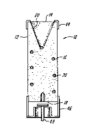
FIGURE 1 is a perspective view of a channel
electron multiplier of the present invention;
FIGURE 2 is a perspective view of an
embodiment of the present invention.
FIGURE 3 is a sectional view taken along
lines 3-3 of FIGURE 1 with additional support and
electrical elements thereon;
--6--
FIGURE 4 is a sectional view, similar to
that shown in FIGUR~ 3, of a modified version of the
channel electron multiplier of the present invention;
FIGURE S is a perspective view of yet
5 another channel electron multiplier of the present
invention; and
FIGURE 6 is a cross-sectional elevation view
along the line 6-6 of FIGURE 5.
Description of the preferred Embodimen~
Referring to FIGURE 1 and 3~ a channel
multiplier constructed in accordance with the present
inYention is shown at 10. It is comprised of a
mono1ithic electrically insulatin~, ceramic
material. It wi11 be appreciated that the problems
15 of reg;stration and seams in the channel passage, as
disc~osed, for e~ample in the above-discussed Patent
Nos. 3,224,927 and 4,095,132, are obviated by the
monolithic body.
In the embodiment shown in FIGURES 1 and 3,
20 the monolithic boay 12 of the multiplier i~
cylindrical in shape. As will be further noted, one
: end of said body may be provided with a cone or
funnel shaped entryway or entry port 14 which evolves
to a hollow passageway or channel 16. The channel 16
25 preferably is three dimensional and may have one or
more turns thereîn which are continuous throughout
the body 12 of the multiplier 10 and ~its the
multiplier 10 at an e~it port at the opposite end 18
of the cylinder shaped body from the entryport 14.
30 It will also be appreciated that the passage of the
channel must be curved in applications where the
multiplier gain is greater than about 1 ~ 106 to
avoid iDstability caused by ~ion feedbacka.
--7--
The surface 20 of the funnel shaped entryway
14 and the hollow passageway 16 is coated with a
semiconducting material having good secondary
emitting properties. Said coating is hereinafter
5 described as a dynode layer.
FIGURE 3 is a modified version of FIGURE 1,
wherein an input collar 44 is press fit onto the
ceramic body 12 and is used to ma~e electrical
contact with entry port 14. An output flange 46 is
10 also pressed onto the ceramic body 12 and is used to
position and hold a signal anode 48 and also to make
electrical contact with e~it port 18.
With reerence to FIGURE 2 the embodiment
shown may be described as a free form channel
15 multiplier. In said embodiment, the multiplier 10,
comprises a tube-like curve~ body 22 having an
enlarged funnel-shaped head 24. A passa~eway 26 is
provided through the curved body 22 and communicates
with the funnel-shaped entrance way 28. It will be
20 appreciated that passageway 26 of FIGURE 2 differs
from passageway 16 of YIGURE 1 in that passageway 26
comprises a two-dimensional passage of less than one
turn. It is believed that the FIGURE 1 embodiment
may be preferable over the FIGURE 2 embodiment
25 depending on volume or packaging considerations. As
in the embodiment of FIGURES 1 and 3, the surface 30
of the passageway 26 and entrance way 28 are coated
with a dynode layer.
FIGURE g discloses a further embodiment of
30 the present invention wherein the channel multiplier
10 has the same internal configuration as that shown
in ~IGURES 1 and 3, but has different e~ternal
configuration in that the ~ody 32 is not in the form
of a cylinder. For reasons to be explained below
~ ~3~
relating to the method of manufacturing the channel
multiplier of the present invention, almost any
desired shape may be employed for said multiplier.
Turning now to FIGURES 5 and 6, a~
5 alternati~e embodiment of the present invention
employing a plurality of hollow passageways or
channels therein is shown generally at 60. Channel
electron multiplier 60 is comprised o~ a unitary or
- monolithic body 62 of ceramic material with a
10 multiplicity of hol~ow passages 64 interconnecting
front and bac~ surfaces 6S, 68 of body 62. It will
be appreciated that passages 64 may ~e straight,
curved in tw~ dimensions, or curved in three
dimensions. Preferably, front and back surfaces 66,
15 68 arP made conductive by metallizing them, while a
dynode layer is coated o~ ~he passageways.
The monolithic ceramic body of the
multiplier o~ the present in~ention may be fabricated
from a Yariety of different materials such as
20 alumina, beryllia, mullite, steatite and the like.
The chosen mat~rial should be compatible with the
dynode layer material both chemically, mechanically
and thermally. It should have a high dielectric
strength and behave as an electrical insulator.
The dynode layer to be used in the present
invention may be one of several types. For esample,
a first type of dynode layer consists of a glass of
the same ~eneric type as used in the manufacture of
conventional channel multipliers. When properly
30 deposited on the inner passa~e walls, rendered
conductive and adequately terminated with conductive
material, it should function as a conventional
channel multiplier. Other materials which give
secondary electron emissive properties may also be
35 employed~
- ~ -
The ceramic bodies for the multiplier of the
present invention are fabricated using "ceramic~
techniques.
In general, a preform in the coniguration
of the desired passageway to be provided therein is
surrounded with a ceramic material such alumina and
pressed at high pressure.
AftPr the body containing the preform has
been pressed, it is processed using standard ceramic
10 techniques, such as bisquing and sintering. The
preform will melt or burn-off during the high
temperature processing thereby leaving a passageway
of the same configuration as ~he preform.
Following shaping, the body is sintered to
15 form a hard, dense body which contains a hollow
passa~e therein in the shape of the previously burnt
out preform. After cooling, the surface of the
hollow ~assage ma~ be coated by known techniques with
a dynode material such as described earlier in this
20 application.
Once the passageway has been coated with a
dynode material and the aperture end and the output
end has been metallized, the body may be fitted with
various electrical and support connections as shown
25 in FIGURE 4 such as an input collar or flange 35, a
ceramic spacer ring 34, transparent faceplate 36
having a photoemission film on its inner surface, an
output flange 38, and ceramic seal 40 with a signal
anode 42 attached thereto. In such configuration as
30 shown in FIGURE 4, the device ~unctions as a
phototube vacuum envelope electron mùltiplier.
While preferred embodiments have been shown
and described, various modifications and
substitutions may be made th~reto without departing
from the spirit and scope of the invention.
Accordingly, it is to be understood that the present
invention has been described by way of illustrations
5 and not limitation.
What is claimed is: