Note : Les descriptions sont présentées dans la langue officielle dans laquelle elles ont été soumises.
THERMAL PRINT HEAD CONTAINING
SUPER-THIN POLYCRYSTALLINE SILICON FILM TRANSISTOR
BACKGROUND OF THE INVENTION
Field of the Invention:
The present invention relates to a thermal
print head having heating resistors which are heated se-
lectively for printing information on a thermosensitive
recording sheet and, more specifically to a thin film
thermal print head having heating resistors and a driving
circuit which are formed through the appllcation of thin-
film techniques.
Description of the Prlor Art:
Mos-t conventlonal thermal print heads of a llne
type of a serial type employ either a direct drive system
. or a diode matrix system for driving the heating resistors
thereof. To form such a thermal print head in a compact
construction, the integral semiconductor chips, such as
IC chips and diodes, are mounted directly on the substrate
of the thermal print head. However, directly ~ounting
semiconductor chips on the substrate is subject to many
restrictions relating to forming a compact thermal print
head and the productivity of the thermal print head
-- 1 -- ~,
~ ~3~
manufacturing processes. Accordingly, an
improved thermal print head has been desired.
BRIEF DESCRIPTION OF THE DRAWINGS
Figure 1 is an enlarged sectional view of a
thermal print head containing a super-thin
polycrystalline silicon film transistor, in a first
embodiment, according to the present invention;
Figure 2 is an enlarged sectional view of a
thermal print head containing a super-thin
polycrystalline silicon film transistor, in a second
em~odiment, according to the present invention;
Figure 3 is an enlarged sectional view of a
thermal print head containing a super-thin
polycrystalline silicon film transistor, in a third
embodiment, according to the present invention;
Figure 4 is an enlarged sectional view of a
thermal print head containing a super-thin
polycrystalline silicon film transi.stor, in a fourth
embodiment, according to the present invention;
Figure 5 is a block diagram showing, by way of
example, the constitution of the circuit o-f a thermal
print head;
Figure 6 is a typical side elevation of a
conventional thermal print head; and
Figure 7 is an enlarged sectional view of a
thermal print head containing a super-thin
polycrystalline silicon film transistor, in a fifth
embodiment, according to the present invention.
As illustrated in Fig. 6, when a semiconductor
chip 102 is mounted on a substrate 101 of a thermal print
head and is sealed with a sealing material 103, the
projecting portion of the sealing material 103 and a
cover 10~ must be positioned outside the paper feeding
space through which a thermosensitive recording sheet is
fed by a platen 105, and hence the reduction of the
distance Wl between the front end of the semiconductor
chip 102 and the platen 105 is limited to a certain
extent, which is an impediment to the reduction in size
of the thermal print head.
On the other hand, the dimension W2 of the
substrate is dependent on the length of the semiconductor
chip 10~ and the wire bonding pitch. Accordingly, the
dimension W2 can be reduced to a certain extent by
employing a LSI chip as the semiconductor chip 102.
However, such a semiconductor chip is expensive.
Furthermore, the least wire bonding pitch is limited to a
value on the order of 150 to 200 ~m. For example, the
dimension W2 is approximately 3 mm when the semiconductor
3 --
chip 102 is a 32-bit driver, and is approximately 7 mm
when the same is a 64-bit driver.
The conventional thermal print head has many
problems such as:
l) low reliability due to many joints formed
by wire bonding, soldering and/or thermocompression
bonding,
2) the semiconductor mounting process
requires expensive equipment, such as a wire bonder and a
resin baking oven, and skilled labor,
3) the necessity of many materials and parts
such as IC chips, gold wires and a die bonding paste
requires many assembling processes and, hence, high
manufacturing cost, and
~ ) IC chips in addition to the semiconductor
chip 102 are necessary when other circuits, for example,
a counter circuit, a temperature sensing circuit and a
memory circuit, are required to be mounted on the
substrate lO1 of the thermal print head.
Japanese Patent Provisional Publication No. 58-
153672 discloses a thin ~ilm thermal print head
comprising a driving amplifier for driving a recording
device, i.e., heating resistors, and recording control
circuit each contalning thin film transistors.
3~j93
: However, in this known thermal print head
having such a driving unit comprising ordinary thin film
transistors, the perimeter of the gate needs to be very
large when the driving unit is used for switching a large
current, because of the low electron mobility lu of the
thin film transistors. Consequently, the size of the
device is increased, which restricts the reduction in
size of the thermal print head. Thus, this known thermal
print head has problems such as large power loss and,
hence, low efficiency due to the large driver ON
resistance, and difficulty in hi~h-speed recording and
i high-gradational recording due to the inferior frequency
~ characteristics of the field effect transistors incapable
I of responding to high-frequency waves of frequencies on
the order of 4 to 6 MHz.
Thus, many restrictions are placed on the
¦ conventional thermal print head in constructing the same
in a compact construction and the conventional thermal
print unit is disadvantageous in respect of the
productivity of the manufacturing process and the
; manufacturing cost. Although another thermal print head
employing a driving unit comprising ordinary thin film
transistors has been proposed, it is difficult to apply
this thermal print head to high-speed printing and high-
,- .,
,.~
gradational reeording due to its inferior
eharaeteristies.
~UMMARY OF T~E INVENTION
Accordingly, it is an objeet of the present
invention to provide a thermal print head eontaining
super-thin polyerystalline silieon film transistors,
having less restrietions on the size of the substrate,
capable of being formed in a compact eonstruction, and
capable of being manufaetured through a mass-produetion
system at a redueed eost.
It is another object of the present invention
to provide a thermal print head containing super-thin
polycrystalline silicon film transistors, capable of
high-speed printing and high-gradational printing.
Aceording to the present invention, a thin
polycrystalline silieon film is formed over an insulating
substrate, a heating resistor and a driving eireuit is
formed by using the polyerystalline silicon film on the
same insulating substrate, and the driving circuit is
constituted by a thin film transistor having a thin
active layer.
The insulating substrate is a silieon substrate
provided, at least in a portion thereo~, with an
insulating layer having at least one thermai resistanee
~ ~3~
layer, a thin polycrystalline silicon layer is formed
over the insulating layer having the thermal resistance
layer, and a heating resistor and a driving circuit is
constituted by using the thin polycrystalline silicon
film.
Furthermore., according to the present
invention, at least one thermal resistance layer is
formed on at least a portion of the insulating silicon
substrate, then a thin polycrystalline silicon layer is
formed over the thermal resistance layer, and then a
heating resistor and a driving circuit are formed by
using the thin polycrystalline silicon layer.
The thin film transistor having a thin active
layer is disclosed in Canadian Patent Application Serial
Nos. 470,775 and 470,776, both filed December 21, 1984,
which have been made previously by the applicant of the
present application. The present invention is one of the
utility inventions made by the practical application of
the thin film transistor having a thin active layer,
previously invented by the applicant of the present
invention.
According to the present invention, since the
driving circuit is formed by using the thin
polycrystalline silicon film formed over an'insulating
substrate, the size of the projection of the driving
-- 7 --
~3~
circuit can be reduced to a value below several microns,
which eliminates restrictions on the size of the
substrate.
Furthermore, since the thickness of the
polycrystalline silicon layer serving as the active layer
or active region of the transistor of the driving circuit
is 800 A or below, which is substantially the same as the
thickness of the depletion layer, the electron mobility ,u
is increased, and thereby a driver chip of several
milliampere to several tens milliampere in capacity
having a minute area can be manufactured. Furthermore,
since the operation frequency of the logic circuit is
comparatively high, the thermal print head is capable of
high-speed printing and high-gradational printing.
Furthermore, according to the present
invention, since the insulating substrate is a highly
heat-conductive silicon substrate, and a 1 to 500 ,um
thick thermal resistance layer, preferably, 10 to 150 ,um
thick thermal resistance layer, is formed over the
insulating substrate so that the thermal conductivity of
the insulating substrate is in an appropriate range, or a
0 to 350 ~m thick second thermal resistance layer is
formed so that the total thickness of the thermal
thickness layer is below 500 ~m, to contro; the heat
eneration of the thermal resistance layer properly and
-- 8
3~ 3
to prevent the excessive accumulation of heat in the
thermal resistance layer and the insulating substrate,
therefore, the heating resistor can be regulated so as to
prevent blurs and irre~ular print density in the print
for improved print quality, and hence the thermal print
head is capable of high-speed printing.
Furthermore, sincè the thermal resistance layer
serving as a heat accumulatiny layer can be easily formed
over the silicon substrate, the substrate forming process
is simplified, and since the driving circuit is formed in
the thin polycrystalline silicon layer, the driving
circuit can be formed in a minute projection, which
eliminates restrictions on the size of the substra-te.
Still further, since the thermal print head of the
present invention is manufactured without resorting to
complex processes including a wire bonding process, the
reliability thereof is enhanced.
The above and other objects, features and
advantages of the present invention will become more
apparent from the following description when taken in
conjunction with the accompanying drawings.
DESCRIPTION OF THE PREFERRED EMBODIMENTS
First, the constitution of the circuit of a
thermal print head containing a super-thin
polycrystalline
silicon film transistor (hereinafter, designated simply
as "thin-film thermal print head") emboaying the present
invention will be described with reference to Fig. 5.
A data signal, namely, a picture signal, is
given through a signal terminal 51 to a shift register
circuit 52. After data for one line has been given to
the shift register circuit 52 according to clock signals
applied to a signal terminal 53, the data is transmitted
by parallel transmission to a latch circui-t 55 in response
to a strobe signal applied to a signal terminal 54 and is
latched by the latch circuit 55. The data latched by the
latch circuit 55 drives a driver device 58 through a gate
circuit 57 in accordance with the instruction of an enable
signal fox determining print timing, applied to a signal
terminal 56 to supply current selectively to heating
resistors 59 to selectively make the heating resis-tors
59 generate heat.
According to the present invention, for example,
the driver device 58 comprises MOS FETs, while other
circuits comprises CMOSs. The MOS FETs and the CMOSs are
formed integrally with the heating resistors in thin-film
transistors comprising a thin polycrystalline silicon
film, a thin conductive film and an insulating film in a
laminated structure. The thin-film transistor is formed
-- 10 --
~3~
in a super thin polycrystalline silicon film transistor
having a source active layer and a drain active layer
formed of a polycrystalline silicon film of 800 A or
below in thickness.
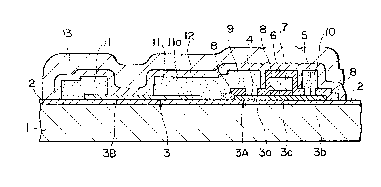
First Embodiment:
Referring to Fig. 1 showing a thin-film thermal
print head, in a first embodiment, according to the pre-
sent invention, a heating resistor is formed of the same
material as the active layer of the MOS FET of a driver
device, and the source and drain of the MOS FET are used
as the electrodes of the heating resis-tor.
In this embodiment, an insulating layer 2 of
SiO2 or the like is formed over the entire surface of the
substrate 1 of a thermal print head, and a thin polycrys-
talline silicon layer 3 is formed over the insulating
layer 2. The substrate 1 may be a quartz plate, a glass
plate, a glazed ceramic plate or a convex plate having
a slightly elevated portion in which a heating resistor
is formed, for example, a partly glazed substrate.
Although the insulating layer 2 is not necessarily needed,
normally, an insulating thermal resistance layer is formea.
The insulating layer 2 serves as a heat accumulating layer
which accumulates heat generated by a heating resistor 3B,
while the substrate 1 serves as a heat conducting layer
-- 11 --
3~
which transmits heat accumulated in the insulating layer
2 to a heat radiating plate. Print quality and the
printing speed of the thermal print head is greatly de-
pendent on the ma-terials forming the substrate 1 and the
insulating layer 2, and the thickness of the insulating
layer 2. In this embodiment, the substrate 1 is formea
of either single crystal silicon or polycrystalline
silicon. Silicon has a thermal conductivity in an appro-
priate range for the heat conducting layer. The insulat-
ing layer 2 is formed of SiO2, which has a comparatively
low thermal conduc-tivity in an appropriate range for the
heat accumulating layer, and has particularly desirable
properties facilitating the formation of a thin film in
a desired thickness. The SiO2 insulating layer 2 may be
formed through an ordinary thermal oxida-tion process in
which the surface of the silicon substrate 1 is oxidized
or a vacuum film forming process such as a sputtering
process. The smaller the thickness of the insulating
layer 2 the better is the print quality. And also, the
greater is the energy consumption of the insulating
layer 2. Therefore, it is not desirable to form the in-
sulating layer 2 in an excessively small thickness.
Accordingly, the SiO2 insulating layer 2 is formed in a
thickness in the range of 1 to 500 ~m appropriate for
- 12 -
optimum heat conduction. When the thickness of the SiO2
insulating layer 2 is 1 ~m or below, the energy consump-
tion of the insulating layer 2 is excessively high and,
when 500 ~m or above, an excessively large amount of heat
is accumulated in the substrate 1 and satisfactory heat
radiation is impossible, which causes the deterioration
of the print quality including blurred printings and
irregular printing density. Although the SiO2 insula-ting
layer 2 may be formed in a thickness in the range of 1 to
500 ~m, practically, it is preferable to form the SiO2
insulating layer 2 in a thickness in the range of 10 to
150 ~m. A cooling plate 24 for radiating the heat trans-
ferred thereto from the substrate l may be attached
adhesively to the backside of the substrate 1 having the
insulating layer 2 over the upper surface thereof with
the film 23 of a flexible adhesive such as a silicon
adhesive as illustrated in Fig. 7 when necessary. The
cooling plate 24 is formed of a material having a large
thermal conductivity, such as aluminum, copper or aluminum
oxide.
The polycrystalline silicon layer 3 is used as
an active layer for forming the thin-film transistors of
the driving circuit, and the heating resistor. The oppo-
site end portions of the polycrystalline silicon layer 3A
3~1 3
for the driving circui-t of the polycrystalline silicon
layer 3 is doped with an n-type impurity to form n-type
regions 3a and 3b having a low resistance. The n-type
regions 3a and 3b serves as a source region 4 and a drain
region 5, respectively. When the MOS FET is in operation,
a channel is formed be-tween -the source region 4 and the
drain region 5 in the polycrystalline silicon layer 3A,
and the region between the source region 4 and the drain
region 5 serves as an active layer 3c.
An insulating gate layer 6 of SiO2 is formed
on the polycrystalline silicon layer 3A. Gate electrodes
7 of doped polycrystalline silicon (DOPO~) are formed on
the insulating gate layer 6. The material o the gate
electrodes 7 is not limited to doped polycrystalline
silicon; the same may be formed of Ta-SiO2, Ta-Si, TaN
or NiCr.
An insulating layer 8 of SiO2 is formed over
the polycrystalline silicon layer 3A and the gate elec-
trodes 7. The insulating layer 8 is provided with
openings through which electrodes 9 and 10 of Al, W, Ti
of Mo connected to the source region 4 and the drain
region 5, respectively, are formed to constitute the
driving circuit.
In the ordinary MOS FET thus constituted, the
- 14 -
33~
thiekness of the polycrystalline silicon layer 3A in
which the channel is formed is on the order of 1500 ~.
However, in the MOS FET of the present invention the
thickness of the polycrystalline silicon layer 3A is as
thin as 800 A or below, and hence the field effec-t elec-
tron mobility ~ is very large, which is inferred to be
due to the thickness of the polyerystalline silieon layer
3A smaller than the thiekness of the ehannel indueed in
the active layer 3e when a gate voltage of an ordinary
magnitude is applied to the gate eleetrode 7. The thiek-
ness of the polyerystalline silieon layer 3A is in the
range of 20 to 800 A, preferably, 200 A.
On the other hand, the polycrystalline silicon
layer forming the active layer 3e is used for forming
heating resistors 3B as well as the driving cireuit.
Lead eleetrodes 11 are eonneeted to the polyerystalline
silieon layer forming the heating resistors 3B in the
proeess for forming the lead electrodes 9 and 10. In
this embodiment, lead eleetrodes lla among the lead elee-
trodes 11 are formed integrally with the lead eleetrcdes
9 of the souree region 4 to connect the driving eireuit
and the heating resistors 3B eleetrically. Wiring of
the driving circuit may be formed in two wiring layers,
for example, a wiring layer of a material having a
3~
comparatively high resistivity containing a wiring for
transmitting signals such as enable signals, latch signals,
data signals and clock signals between the active ele-
ments of the driving circuit, and a wiring layer of the
same material as the source and drain electrodes contain-
ing a wiring for VHI GH, VD and GD-
An oxidation resistant layer 12 and an abrasionresistant layer 13 are formed over the heating resistors
and the driving circuit. The oxidation resistant layer
12 and the abrasion resistant layer 13 function as a
protective film for the heating resistances 3B and as a
passivation film for the FETs of the driving circuit.
In the thermal print head thus constituted,
since the drivers of the driving circuit are thin-film
transistors, the dimension t in Fig. 6 namely, the height
of the drivers on the substrate, is substantially zero
(several microns or less). Accordingly, there is not any
restriction on the construction of the thermal print head
~ith respect to the paper feed space. Further, the pos-
sibility of forming the driving circuit at an optional
position enables reduction in size of the thermal print
head.
Furthermore, the driving circuit and the heat-
ing resistors are electrically interconnected by wiring
- 16 -
patterns of thin films, which are free from restric-tions
on the pitch of wiring lines and, hence, dimensional
restrictions, without requiring wire bonding process,
complex processes, the use of expensive equipments and
materials for wire bonding. Particularly, the thermal
print head has high reliability because the thermal prin-t
head does not include any IC chip and, hence any junction.
Still further, since the heating resistors and
the active elements of the driving circuit are formea
simultaneously through the same process on the same sub-
strate, the manufac-turing cos-t of the thermal print head
remains subs-tantially constant regardless of the design
of the circuit, which is highly advantageous in the
practical application of the thermal print head.
Particularly, when the substrate 1 is a silicon
substrate, and the insulating layer 2 is a SiO2 layer of
a thickness in the range of 1 to 500 ~m, preferably, 10
to 150 ~m, heat accumulation in the vicinity of the heat-
ing resistors 2 can be controlled properly, and thereby
print quality and printing speed are improved.
Although the present invention has been de-
scribed with reference to a first embodiment thereof in
which the active layers of the MOS FETs of the driving
circuit are used as the heating resistors, the present
- 17 -
~ ~3~ 3
invention is not limited thereto and, naturally, many
variations and changes are possible therein. Further
embodiments of the present invention will be described
hereinafter. In the following description, those parts
that are the same or corresponding to those of the first
embodiment are designated by like reference characters
throughout and the description thereof will be omitted
to avoid duplication.
Second ~mbodiment (Fig. 2):
The gate electrodes 7 of FETs and heating
resistors 21 are formed simultaneously of the same gate
material. The lead electrodes o~ the heating resistors
21, and the respective lead electrodes 9 and 10 of the
source region 4 and the drain region 5, similarly to
those of the first embodiment, are formed simultaneously
of the same electrode material.
Third Embodiment (Fig. 3):
A polycrystalline silicon layer 3 for forming
the active layer 3c of FETs is used, similarly -to that of
the first embodiment shown in Fig. 1, for forming heating
resistors 3B, and an insulating layer 8 is functions also
as an oxidation resistant layer for the heating resistors
3~. Accordingly, any particular oxidation resistant
- 18 -
layer, such as the oxidation resistant layers 12 of the
first and second embodiments shown in Figs. 1 and 2,
respectively, need not be formed over the heating re-
sistors 3B, and only an abrasion resistant layer 13 is
formed over the driving circuit and the heating resistors
3B.
Fourth Embodiment (Fig. 4):
Hea-ting resistors 21, similarly to those of the
second embodiment shown in Fig. 2, are formed of the same
gate material forming the gate electrodes 7 of FETs, and
an insulating layer 8 functions also as an oxidation
resistant layer for the heating resistors 21. Accordingly,
the fourth embodiment, similarly to the third embodiment
shown in Fig. 3, does no-t need any particular oxidation
resistant layer 12. The heating resistors, similarly to
those of the conventional thermal print head, may be
formed of Ta-SiO2, Ta-Si, TaN or NiCr, and the heating
resistors may be connected to -the thin-film -transistors,
respectively, by a wiring pattern of the electrodes of
the thin-film transistors.
In the foregoing embodiments, the heating
resistors 3B are formed on the insulating layer 2, i.e.,
the thermal resistance layer, formed over the flat sub-
strate to control heat accumulation in the vicinity of
- 19 -
the heating resistors 3B properly, and thereby print
quality can be improved to a satisfactory extent.
However, for the further improvement of print quality,
it is possible to form a convex SiO2 layer as a second
thermal resis-tance layer 22 under the heating resistors
3B as illustrated in Fig. 7 to enable the appropriate
contact of the heating resistors 3B with the thermosensi-
tive recording sheet. The convex second thermal resist-
ance layer 22 is formed through a vacuum thin-film form-
ing technique, such as a spu-ttering process.
When two or more thermal resistance layers are
formed as mentioned above, preferably, the total thick-
ness ~f the thermal resistance layers, similarly to those
of the foregoing embodiments, is in the range of 1 to
500 ~m. Accordingly, it is preferable that the total
thickness of the thermal resistance layer 2 and the second
thermal resistance layer 22 of the embodiment shown in
Fig. 7 also is in the range of 1 to 500 ~m. Therefore,
the thickness of the second thermal resistance layer 22
is dependent on the thickness of the thermal resistance
layer 2 formed over the substrate 1. However, the prefer-
able thickness of the second thermal resistance layer 22
is in the range of zero to 350 ~m. The parts of the em-
bodiment shown in Fig. 7 like or corresponding to those
- 20 -
of the foregoing embodiments are designated b~ like refer-
ence characters and the description thereof is omitted to
avoid duplication.
As apparent from the foregoing description, the
thermal print head according to the present invention
comprises heating resistors and a driving circuit formed
on the same substrate and interconnected by wiring pat-
terns formed of a gate material and an electrode material,
respectively, without requiring a wire bonding process.
Therefore, the thermal print head production line is able
to operate at a high productivity and the thermal print
head of the present invention has a high reliability.
Furthermore, since the driving circuit comprises
thin-film transistors and the height of the -thin-film
transistors on the substrate is very small (several
microns or less), there is not any restriction on the
disposition of the thermal print head relative to the
platen, and the employment of the thin-film transistors
is very advantageous to the reduction in size of the
thermal print head.
Still further, since the thickness of the active
layer of the thin-film transistors of the driving circuit
is as small as ~00 A and hence the electron mobility ~ is
very high, the thin-film transistors, namely, driving
- 21 -
3~j9 ~
devices, may be of a very small area, which also is ad-
vantageous to the reduction in slze of the thermal print
head.
Moreover, forming the active layer in a thin
film is h1ghly effective for improving the printing
characteristics of the thermal print head in the practical
application thereof as well as for -the reduction in size
of the thermal head. For example, the thin-film active
layer reduces the on-resistance of the driver device and,
hence the power loss, and thereby the power efficiency
is improved remarkably. Since the frequency character-
istics of the FETs can be improved, high-speed printing
and high-gradational printing are possible.
Still further, when the insulating substrate is
formed of silicon having a high thermal conductivity and
the thermal resistance layer is formed of SiO2 over the
surface of the insulating substrate, heat accumulation in
the vicinity of the heating resistors can be controlled
properly, an excessive amount of heat will not be accu-
mulated in the thermal resistance layer and the insulating
substrate, and blurs and irregular density in the printing
are eliminated to improve the print quality.
Particularly, when the convex second thermal
resistance layer is formed under the heating resistors,
- 22 -
~8~ 3
the state of contact between the heating resistors and
the thermosensitive recording sheet is improved, and
; thereby -the print quality is further improved.
:
: "
.
,
- 23 -