Note : Les descriptions sont présentées dans la langue officielle dans laquelle elles ont été soumises.
~J ~2B4~i9Z
FIELD OF TH~ INVENTION
This invention relates to the fabrication of a planar
multilayer interconnection system for multichip high performance
semiconductor packaging.
BACKGROUND OF THE INVENTION
Very Large Scale Integration (VLSI) and Ultra Large Scale
Integration (ULSI) devices in semiconductor technology are
expected to result in significant performance improvementS in
systems based on such devices. However, many of the advantages
of such devices will be lost without significant improvements in
device packaging techniques. A number of new designs, materials
and processes capable of providing high density multilayer
interconnections with controlled electrical characteristics have
been proposed. These include high density printed circuit
boards, cofired multilayer ceramics, customized multilayer cop-
per/polyimide interconnections built on cofired ceramic sub-
strates and wafer scale integration using semiconductor inte-
grated circuit (IC) processing. One of the most versatile and
cost effective of the interconnection technologies is a sequen-
tially built multilayer structure of metal conductor and die'ec-
tric material using a substrate such as silicon, ceramic or mo-
lybdenum.
Howe~er, one of the problems encountered in the multilaye-
structure is the ability to obtain continuity of the upper 'àye~
metal films and the integrity of the dielectric insulating ia~-
1~84692
over the step formed by the underlying metallization pattern.The problem is caused by the protrusion of the metallization
pattern that results in an increase in the degree of unevenness
as the number of metallization layers increases.
Another problem relates to the adhesion between the metal
conductor and the dielectric. For instance, the adhesion
between a copper conductor and polyimide dielectric is enhanced
by the use of a thin layer of chromium, titanium, titanium tung-
sten alloy or nickel between them. This thin layer of metal
also serves as a corrosion barrier for the copper conductor.
The two techniques previously known in the art, the subtractive
and the additive process, were unable to provide a suitable
layer between the conductor and the dielectric. The subtractive
process did not provide a completely sealed and corrosion resis-
tant copper conductor; and although the additive process formed ;
a completely sealed and corrosion resistant copper conductor,
extra processing steps were required, which resulted in extra
expense.
SUMMARY OF THE I NVENT I ON
The present invention provides many advantages over theprior methods. First, the present invention provides a fully
planar, multilayer structure with completely sealed and cor.o-
sion resi,stant conductors separated by polyimide dielectric :a -
ers. The present invention also provides this structure ~ ^c_~
the use of the additional processing steps used in the prior
-2-
r~
128469Z
art. This structure is a high density packaging that is useful
with VLSI and ULSI devices.
Additional advantages provided by this invention are set
jforth, in part, in the following description. Other advantages
will be obvious from the following description, or may become
apparent by practice of the invention. The appended claims par-
ticularly point out how the advantages of the invention can be
attained.
To obtain the advantages of the present invention, then, a
layer of a planar multilayer interconnection system is fabri-
cated using a method comprising: ;
a) forming a dielectric sub-layer overlaying a base
layer, the dielectric sub-layer being nonsoluble after the layer
is cured;
b) forming a sacrificial sub-layer overlaying the
dielectric sub-layer, the sacrificial sub-layer being soluble
after the layer is cured;
c) removing a portion of the sacrificial sub-layer
to expose a portion of the dielectric sub-layer;
d) removing the exposed portion of the dielectric
sub-layer and a selected portion surrounding the exposed portion
of the dielectric sub-layer to expose a portion of the base
layer, removal of the selected portion leaving an exposed por-
tion of the sacrificial sub-layer overhanging the exposed por-
tion of the base layer;
--3--
il ~ 1~84692
.1 :
~1 e) depositing a first conductive adhesive sub-layer
~I overlaying the dielectric and sacrificial sub-layers and the
exposed area of the base layer without overlaying the exposed
overhang portion facing the base layer of the sacrificial sub-
layer;
f) depositing a conductive seeding sub-layer
overlaying the first conductive adhesive sub-layer:
g) removing the sacrificial sub-layer and the first
conductive adhesive sub-layer and the conductive seeding sub-
layer in contact with the sacrificial sub-layer;
h) forming a conductor sub-layer by electrolessly
plating a conductor sub-layer onto the seeding sub-layer; and
i) forming a second conductive adhesive sub-layer by
electrolessly plating the second adhesive sub-layer onto the
conductor sub-layer to form a surface which is planar with the
dielectric sub-layer.
One preferred embodiment of the invention comprises a meth-
od for fabricating a layer of a planar multilayer interconnec-
tion system comprising:
a) forming a polyimide sub-layer overlaying a base
layer, the polyimide sub-layer being nonsoluble after the layer
is cured;
, b) forming a metallic sub-layer overl.aying the
polyimide sub-layer;
c) forming a sacrificial sub-layer overlaying the
` J 1~84692
metallic sub-layer, the sacrific;al sub-layer being selected
from polyimides which are soluble after the layer is cured;
d) removing a portion of the sacrificial sub-layer
to expose a portion of the metal].ic sub-layer;
e) removing the exposed portion of said metallic
sub-layer to expose a portion of the polyimide sub-layer;
f) removing the exposed portion of the polyimide
sub-layer and a selected portion surrounding the exposed portion
of the polyimide sub-layer to expose a portion of the base
layer, removal of the selected portion leaving an exposed por-
tion of the metallic sub-layer and the sacrificial sub-layer
overhanging the exposed portion of the base layer;
g) removing the portion of said metallic sub-layer
overhanging the exposed portion of the base layer;
h) depositing a first conductive adhesive sub-layer
overlaying the polyimide and sacrificial sub-layers and the
exposed area of the base layer without overlaying the exposed
overhang portion facing the base layer of the sacrificial sub-
layer;
i) depositing a conductive seeding sub-layer
overlaying the first conductive adhesive sub-layer;
j) removing the sacrificial sub-layer and the firsr
conduct.ive adhesive sub-layer and the conductive seeding sub-
layer in contact ~ith the sacrificial sub-layer;
k) removing the metallic sub-layer;
~284692
!¦ ,
1) forming a conductor sub-layer by electrolessly
plating a conductor sub-layer onto the conductive seeding sub-
layer; and
m) forming a second conductive adhesive sub-layer by
electrolessly plating the second conductive adhesive sub-layer
onto the conductor sub-layer to form a surface which is planar
with the polyimide sub-layer.
In another preferred embodiment, the present invention com-
prises a method for fabricating a layer of a planar multilayer
interconnection system comprising:
a) forming a silicon dioxide sub-layer overlaying a
base layer;
b) forming a sacrificial sub-layer overlaying the
silicon dioxide sub-layer, the sacrificial sub-layer being solu-
ble after the layer is cured;
c) removing a portion of the sacrificial sub-layer
to expose a portion of the silicon dioxide sub-layer;
d) removing the exposed portion of the silicon
dioxide sub-layer and a selected portion surrounding the exposed
portion of the silicon dioxide sub-layer to expose a portion o~
the base layer, removal of the selected portion leaving an
exposed portion of the sacrificial sub-layer overhanging the
exposed portion of the base layer;
e) depositing a first conductive adhesive sub-laye~
overlaying the silicon dioxide and sacrificial sub-layers and
~ ~ 12~34~9~
the exposed area of the base layer without overlaying the
exposed overhang portion facing the base layer of the sacrifi-
cial sub-layer:
f) depositing a conductive seeding sub-layer
overlaying the first conductive adhesive sub-layer
g) removing the sacrificial sub-layer and the first
conductive adhesive sub-layer and the conductive seeding sub-
layer in contact with the sacrificial sub-layer;
h) forming a conductor sub-layer by electrolessly
plating a conductor sub-layer onto the seeding sub-layer: and
i) forming a second conductive adhesive sub-layer by ;
electrolessly plating the second adhesive sub-layer onto the
conductor sub-layer to form a surface which is planar with the
silicon dioxide sub-layer.
The accompanying drawings, which constitute a part of this
specification, illustrate one embodiment of the inventi-on and
serve to explain the principles of the invention.
BRIEF DESCRIPTION OF THE DRAWINGS
Fig. 1-12 are cross-sectional views of one embodiment of
one layer of the multilayer interconnection system in various
staqes of completion.
Fig. 13-14 are cross-sectional views showing several com-
plete layers of the multilayer interconnection system.
Fig. 15-19 are cross-sectional views of another embodimenr
of one layer of the multilayer interconnection system in var:o~s
stages of completion.
128~g2
DETAILED DESCRIPTION OF THE INVENTION
Referring to Fig. 1, a base layer 10, which can either be a
previously formed layer or a substrate such as silicon, ceramic,
or molybdenum, is thoroughly cleaned to remove all contaminants
and then subjected to a dehydration bake to remove the moisture
from the surface of the base layer. Base layer 10 is then coated
with an adhesion promoter for optimum adhesion before the coating
of the dielectric sub-layer 12.
After this preparation step, the first step in forming a
layer of the multilayer interconnection system, as shown in Fig.
1, comprises forming a dielectric sub-layer 12 overlaying the
base layer lO. Any dielectric material can be used for this sub-
layer as long as the sub-layer is nonsoluble after the layer is
cured. The preferred dielectric sub-layer material is a
photosensitive type polyimide which is nonsoluble after curing of
the layer or a silicon dioxide, which is nonsoluble. Typical
photosensitive polyimides that can be used include PROBIMIDE 300*
series manufactured by CIBA-GEIGY Corporation in California or
Selectilux HTR 3* manufactured by EM Industries, Inc. in New
York. The dielectric sub-layer 12 can be applied using any
conventional method, such as a spin or spray coating process.
If the dielectric material 12 used for the first dielectric
sub-layer is a polyimide, then the polyimide must be softbaked.
This is a mild heat treatment used to set the polyimide and
remove excess solvent.
* TRADE MARK
1~8469Z
After softbake, if the dielectric materizl 12 is a
photosensitive material and if the sacrificial sub-layer will
be patterned using ultraviolet light, then che next step in
forming the layer is forming a metallic sub-layer 14
overlaying the dielectric sub-layer 12, as shown in Fig. 2, to
shield the dielectric sub-layer 12. Although any metal which
will shield ultraviolet light can be used, the preferred metal
is titanium. The metal is deposited as a film 14 with
thickness suitable for shielding ultraviolet light. Generally
a thickness of about 5,000 to 10,000 angstoms is sufficient.
This metallic sub-layer is formed at a substrate temperature
equal to or less than the-softbake temperature of the
polyimide sub-layer to prevent premature curing of the
polyimide sub-layer.
If the dielectric is not photosensitive, such as silicon
dioxide, then no metallic sub-layer is necessary and the next
sub-layer is applied directly over the dielectic sub-layer.
Thereafter, as shown in Fig. 3 and 15, a sacrificial sub-
layer 16 is formed which is overlaying the dielectric sub-
layer 12, and, if present, the metallic sub-layer 14. Any
conventional material used in the semiconductor art as a
sacrificial layer can be used within the scope of the claimed
invention. This sacrificial sub-layer, however, must be
soluble after the layer is cured. Preferred materials for
this sub-layer 16
_g_
J 1284692
include photosensitive material such as photoresist or
polyimides such as pRoBrMIDE 400 series manufactured by
CIBA-GEIGY Corporation. This sub-layer can also be applied by
spin or spray coating on the surface. The sacrificial sub-layer
is then softbaked.
The next step of the process involves removing a portion of
the sacrificial sub-layer 16 to expose a portion of the
underlying sub-layer, which in Fig. 5 is metallic sub-layer 14
and in Fig. 16 is the dielectric sub-layer 12. The sacrificial
layer is removed according to the desired conductor configura-
tion. As will be evident from the following disclosure, any
planar configuration can be made according to the claimed inven-
tion, resulting in conductors on different layers crossing one
another at various angles.
Although any conventional method can be used to remove the . ,
sacrificial layers, since the preferred materials are
photosensitive, removal of the layers in the preferred embodi-
ment, as shown in Fig. 4, is accomplished by exposing the sub-
layer 16 to ultraviolet light using a mask consisting of opaque
and transparent regions 18A and 18B.
Photosensitive polyimides and photoresists can be negatlve
or positive acting and either can be used within the scope of
this invention. ~he commonly available photosensitive
polyimides are negative acting while photoresists are either
positive or negative acting. ;n the event a negative actins
--10--
,~ 128A6g~
material is used, 18A is opaque and after exposing the sub-layer
to ultraviolet light through the mask, the portion of the sub-
i layer underneath region 18A is removed from sub-layer 16 using
conventional techniques, such as contacting with a developer.
The next step of the process comprises removing, if pres-
ent, the exposed portion of the metallic sub-layer 14 to expose
a portion of the dielectric sub-layer 12. This is shown in
Fig. 6. This portion of the metallic sub-layer can be removed
using any conventional method, such as etching away the metallic
sub-layer using a dilute hydrofluoric (HF) acid.
Removal of a portion of the metallic sub-layer 14 exposes a
portion of the dielectric sub-layer 12. The next process step
comprises removing the exposed portion of the-dielectric sub-
layer and a selected portion surrounding the exposed portion of
the dielectric sub-layer to expose a portion of the base layer.
The removal of the selected portion leaves an exposed portion of
the metallic sub-layer, if present, and the sacrificial sub-
layer overhanging the exposed portion of the base layer. This
is shown in Fig. 7 and in Fig. 16.
If photosensitive material is used for the dielectric sub-
layer 12, it is preferred that sub-layer 12 be negative acting.
In that case, since it is not exposed to the ultraviolet light
¦ because of the metallic sub-layer 14, a suitable developer ~i :
remove the exposed portion of sub-layer 12.
1284692
If photosensitive material is no1: used for the dielectric
sub-layer, such as when the dielectric material is silicon
dioxide, this material can be etched using a suitable
solution, such as a hydrogen fluoride based acid.
It is important in this step that the method used to
remove sub-layer 12 does not remove any of sub-layer 16. This
can be achieved either by selecting a removal method that will
not remove the sacrificial sub-layer or by treating the
sacrificial sub-layer 16 so that the method being used does
not remove this sub-layer. In one preferred embodiment, the
sacrificial sub-layer is exposed to ultraviolet light so that
the photosensitivity of the sacrificial sub-layer prevents its
removal. In another preferred embodiment, the dieletric sub-
layer is removed by a solution that will not remove the
sacrificial sub-layer, such as when the solution is a hydrogen
fluoride based acid and the sacrifici~l layer is photoresist.
Removing a portion of sub-layer 12 exposes base layer 10,
as well as selected portions of sub-layer 12 surrounding the
exposed portion. According to the present invention, part of
these selected portions are removed. In the preferred
embodiment, this is accomplished by using the same method used
to remove the exposed portion of the dielectric sub-layer.
Preferably, the side portions are removed so as to provide an
exposed overhanging portion having a lateral depth ranging
from 3 micrometers to 7 micrometers per side, as shown in Fig.
7 and 16.
-12-
J 1~84692
Curing of the layer is done at various times depending upon
'the materials used in the sub-layers. When the dielectric
sub-layer is a polyimide, the polyimide is cured after the above
removal steps. The preferred polyimide materials used in the
present invention for sub-layers 12 and 16 are cured at tempera-
ture ranging from about 275C to about 320C.
When the dielectric sub-layer is silicon dioxide, curing of
the layer is done prior to etching the silicon dioxide layer,
since the conventional etchant for silicon dioxide would attack
the uncured sacrificial sub-layer.
The next step in the process comprises removing the portion
of the metallic sub-layer overhanging the exposed portion of the
base layer, if present, as shown in Fig. 8. The overhang of the
metallic sub-layer 14 can be removed in any conventional manner.
In the preferred embodiment, the metallic sub-layer is etched in
a dilute HF acid to expose the lower surface of the sacrificial
sub-layer.
After removing a portion of the metallic sub-layer, a fi.st
conductive adhesive sub-layer 20A and 20B is deposited so as to
overlay the sacrificial and dielectric sub-layers and the
exposed area of the base layer without overlaying the exposeà
overhang portion of the sacrificial sub-layer facing the base
layer. T,his is shown in Fig. 9 and 17. The first conduc~i;e
adhesive material aids in the adhesion bet~een the conduc~o~ a~~
the base or dielectric sub-layer. In the preferred embodime,-
chromium (Cr) is used as the first conductive adhesive mater:~ .
~84692
After forming the first conductive adhesive material, a
conductive seeding sub-layer 22A and 22B is deposited to overlay
~the exposed surface of the first conductive adhesive material,
~also shown by Fig. 9 and 17. Any conductive material can be
used. Preferably copper (Cu) is used.
The first conductive adhesive material and conductive
seeding sub-layer are preferably deposited by cold sputtering
deposition. Cold sputtering insures that the exposed overhang
portion of the sacrificial sub-layer facing the substrate re-
mains uncovered and that there is a discontinuity in the first
conductive adhesive and conductive seeding sub-layers at the
overhangs. It also insures that the sidewalls of the selected
portions of the dielectric sub-layer are covered with the first
conductive adhesive and conductive seeding sub-layers, as shown
in Fig. 9 and 17. Cold sputtering deposition is preferably per-
formed in-situ using a temperature less than 100 degrees Cel-
siuS.
After the formation of the conductive seeding sub-layer,
the sacrificial sub-layer is removed, as shown in Fig. 10 and
18. Removing this sub-layer also thereby removes the first con-
ductive adhesive sub-layer and the conductive seeding sub-layer
in contact with the sacrificial sub-layer.
In t~e preferred embodiment of the invention, the sac! f:-
cial sub-layer is a soluble polyimide or photoresist, which rr~-
mains soluble after curing. As disclosed earlier, this type o-
-14-
l,ZB~9~
sacrificial material is well known in the art. Since the sacri-
ficial sub-layer 16 is soluble, the sandwich structure of the
first conductive adhesive sub-layer 20B and the conductive
seeding sub-layer 22B that is formed over the upper surface of
the sacrificial sub-layer 16 is lifted off by immersing the sam-
ple in an ultrasonic agitated solution of solvent, such as
methylene chloride or chloroform for polyimide and acetone for
positive photoresist, resulting in the layer as shown in Fig. 10
and 18. The solvent should not attack the conductive adhesive
or the conductive seeding sub-layers.
The contact of the solution with the soluble sacrificial
sub-layer 16, as in the preferred embodiment, is facilitated by
the presents of overhangs. The solution enters the overhangs
where the bottom surface of the soluble sacrificial sub-layer 16
is exposed and the ultrasonic agitation enhances the liftoff
action and results in the removal of the first conductive adhe-
sive sub-layer 20B as well as the conductive seeding sub-layer
228, as shown in Fig. 10 and 18. The first conductive adhesive
sub-layer 20A and conductive seeding sub-layer 22A which are in
contact with the upper surface of the base layer 10 and the sice
portions of the dielectric sub-layer 12 remain.
The metallic sub-layer 14, if present, can then be removeà
by an etchant which etches the material used in the metallic
sub-layer preferentially to the conductive seeding sub-laye.
material, as shown in Fig. 11. Again, where the metallic
sub-layer is titanium, a dilute hydrofluoric acid can be used.
~
lZ8~69;2
Final curing, if necessary, of the dielectric sub-layer 12
¦ can be performed at this point. The material used in one pre-
ferred embodiment, a photosensitive polyimide, is cured in a
vacuum at a temperature of about 400 degrees Celsius for 1-2
hours. A vacuum cure is preferred so as to retard the oxidation
of the conductive seeding sub-layer 22A. This will not affect
the pattern resolution.
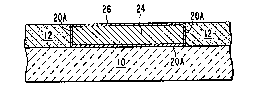
A conductor sub-layer 24 is then formed by electrolessly
plating the conductor material onto the conductive seeding sub-
layer 22A, as shown in Fig. 12 and 19. Electroless plating in-
volves immersing the layer into a bath of conductor material and
is a well known process in the printed wire board art. While
any conductor material can be used, the preferred conductor
material is copper.
A second conductive adhesive sub-layer 26 can then be
electrolessly plated onto the conductor sub-layer 24, completing
a single layer of the multilayer interconnection system, as
shown in Fig. 12 and 19. In the preferred embodiment of the
invention, the second conductive adhesive sub-layer is nickel
(Ni).
This completes a single layer of the interconnection sys-
tem, which comprises a completely sealed conductor sub-layer
which is recessed in a cured dielectric sub-layer 12. The s~--
face of the conductor sub-layer coincides substantially ~ith
that of the dielectric sub-layer.
12'84~g2
It will be apparent that the invention is not restricted to
the description above. For instance, the second dielectric sub-
layer 16 can be a nonphotosensitive soluble material such as
PROBIMIDE 200 series manufactured by CIBA-GEIGY Corporation. In
this case, a negative photoresist and oxygen plasma can be used
to define the pattern. The metallic sub-layer 14 and conductor
materials can be other metallic materials depending upon the
applications.
By applying a new sub-layer of dielectric material and re-
peating the procedures described in Fig. 1 through Fig. 12, or
Fig. 15 through Fig. 19, a planar multilayer interconnection
system consisting of completely sealed and corrosion resistant
copper power planes and signal lines electrically separated by
dielectric layers and interconnected by solid vias can be real-
ized. The layers containing vias are formed using the same
method as above, except that smaller conductor sub-layers are
formed. An array of pretested high performance IC chips can
then be directly attached on and interconnected by this
multilayer system. Fig. 13 shows a cross-sectional view of two
conductor sub-layers interconnected to each other and connected
to the substrate through solid vias. Fig. 14 shows a cross-
sectional view of two conductor sub-layers interconnected by
solid vias but isolated from the substrate.