Note : Les descriptions sont présentées dans la langue officielle dans laquelle elles ont été soumises.
~53~
1 A METHOD AND DEVICE FOR DRIVING
SEMICONDUCTOR POWER COMPONENTS
3 TECHNIC~L FIELD
4 The invention relates to a method and device for driving
semiconductor power components. In particular, the invention
6 relates to a method and a device that transmits, via the same
7 pulse sequence, the control power and control information for
8 driving semiconductor power components.
sAcKGRouND OF THE INVENTION
., . _ . . . _ _ . .
11 The control of semiconductor power components used in
12 power electronics equipment generally requires a separation of
13 potentials to insulate the control section from the power section.
14 In conventional thyristors used as semiconductor power components,
the potential separation is accomplished by means of a pulse
16 transformer which feeds the control current directly to the
17 gate-cathode path, i.e., the control path of the thyristor. In
18 power transistors and thyristors which can be disconnected on the
19 control current side, i.e., GTO thyristors, the cost for
potential-separated control has risen sharply. In general,
21 control currents in pulse form of both polarities are required,
22 for instance, a positive pulse fox swi-tching on and a negative
23 pulse for switching off the semiconductor power component. In
24 addition, the control currents and voltages, respectively, must be
present during the "on" and "off" times of the semiconductor power
26 component, for instance, a positive control current during the
27 "on" time and a negative control voltage during the "off" time.
28 Japanese Patent A 57-12 62 70(A) discloses a device in
29 which one of the secondary windings of a first transformer is
connected via rect;fiexs directly to the gate-cathode path of a
1 GTO thyristor. The positive control current is fed-in during the
2 "on" time via this first secondary winding. Via the second
3 secondary winding, a capacitor is charged as an auxiliary voltage
4 source which can be discharged via a transistox to the primary
S winding of a second transformer. The secondary winding of the
6 second transformer is also connected to the gate-cathode path of
7 the GTO thyristor for feeding-in, via diodes, a negative
8 disconnect current. With this circuit arrangement, the current
9 slope of the control currents is limited by the leakage
inductances of both pulse transformers. This leads to
11 difficulties especially in the case of stringent requirements as
12 to the insulation voltage and in the control of high-power
13 semiconductor components.
14 Another control unit for the potential-separated control
of power transistors is known in which the control information,
16 i.e., the command for switching a power transistor on or off with
17 separated potentials, is transmitted by optoelectronic means. The
18 control information drives a pulse amplifier which connects
19 alternatingly two auxiliary voltage sources with opposite
polarities to the gate-emitter path of a power transistor. The
21 auxiliary voltage sources, which also supply power to the pulse
22 amplifier, are likewise separated as to potential.
23 Disadvantageously, this type of control unit is a very costly
24 device.
Thus, the problem arises to develop a method and device
26 for potential-separated control of semiconductor power components
27 in such a manner that the cost for the potential-separated
28 transmission of the control power as well as the control
29 information is reduced.
--2--
~2~3~l
1 S~MMARY OF THE INVENTION
2 According to the invention, this problem is obviated by
3 a method for driving a semiconductor power component, comprising
4 the steps of:
a. impressing control information for the component on
6 a pulse sequence containing the control power for the component;
7 b. transmitting the pulse sequence to the component to
8 drive the component in a manner so as to separate the respective
9 potentials of the control power and control information; and
c. recovering the control information from the pulse
11 sequence and delivering the control information to the component.
12 In the method according to the invention, the control
13 power as well as the control information is transmitted by the
14 same pulse sequence. Therefore, only one insulating path between
the control section and the power section of a semiconductor power
16 component is required. A pulse transformer, which can provide the
17 potential-separation transmission, can furthermore be designed for
18 a high insulating voltage and small volume since a large leakage
19 inductance is permissable.
It is of advantage to subject the pulse sequence to
21 pulse-width modulation or pulse-frequency modulation. Pulse-width
22 modulation has been found to be particularly advantageous because
23 it simplifies the circuit design by requiring only a simple
24 demodulator with a lowpass filter followed by a comparator
circuit. In addition, it is possible to compensate the load
26 dependence of the control voltages, which occurs because of
27 possible different loads during the "on" and loff" states, by a
28 suitably chosen pulse-to-pause ratio. Further, a reliable
29 switching state can be assigned to the failure of the arrival of
the pulse sequence with pulse-width modulation. If, for instance,
32~
1 a smaller pulse-pause ratio is assigned to the "off" state than
2 the "on" state, automatic opening of a connected semiconductor
3 switch can be realized if the pulse sequence is absent.
4 A device for carrying out the method comprises:
a. means for impressing control information for the
6 component on a pulse sequence containing the control power for the
7 component;
8 b. means for transmitting the pulse sequence to the
9 component to drive the component and for separating the respective
1 potentials of the control power and control information;
11 c. means for recovering the control information from
12 the pulse sequence and delivering the control information to the
13 Component-
14
BRIEF DESCRIPTION OF THE DRAWINGS
16 For a better understanding of the invention, reference
17 is made to the following description of an exemplary embodiment
18 thereof, and to the accompanying drawing, wherein:
19 Fig. 1 is an electrical schematic diagram of a control
section for driving semiconductor power components according to
21 the method of the invention.
22
23 DETAILED DESCRIPTION
-
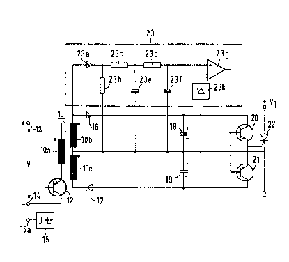
24 Fig. 1 shows an electrical circuit diagram of a control
section which is operated according to the method of the
26 invention. A pulse transformer 10 has a primary winding 10a and
27 two secondary windings 10b, 10c. The primary winding 10a of the
28 pulse transformer 10 is connected at one end to the emitter of a
29 transistor 12 and at the other end to the positive terminal 13 of
a d-c voltage source V. The collector of the transistor 12 is
i3;;~ ~
1 connected to the negative terminal 14 of the d-c voltage source V.
2 The base of the transistor 12 is addressed by a modulating stage
3 15 which receives control pulses at a control input 15a~ The
4 modulating stage 15, which can be used, for instance, in an R-C
oscillator, generates a width-modulated pulse sequence having a
6 pulse frequency of about 1 MHz. With pulse-width modulation, the
7 trailing flanks of the individual control pulses are modulated in
8 such a manner that a small pulse pause is assigned to state "1" of
9 the firing signals (corresponding to the command "thyristor on")
and a large pulse pause is assigned to state "0" (corresponding to
11 the command "thyristor off").
12 One end of each secondary winding 10b, 10c (i.e., the
13 tap of each secondary winding) of the pulse transformer 10 is
1~ connected, via a respective diode 16, 17, to one end of a
respective capacitor 18, 19, each serving as an auxiliary voltage
16 source, and to the collector of a respective transistor 20, 21.
17 The transistors 20, 21 form the pulse amplifier and are tied
18 together in a push-pull arrangement with each base tied to the
19 other and each emitter connected to the gate-cathode pathof a GTO
thyristor 22. The cathode of the thyristor 22 is connected to the
21 negative terminal of a d-c voltage source Vl;to the junction point
22 Of the two secondary windings 10b, 10c, which has zero potential;
23 and to the ends of the capacitors 18, 19 not already connected to
24 the windings 10b, 10c. The anode of the thyristor 22 is tied to
the positive terminal.
26 The tap of one of the secondary windings 10b is also
27 tied to a demodulation stage 23 which, in the embodiment example
28 shown, comprises a lowpass filter circuit followed by a comparator
29 circuit. The tap of the one secondary winding 10b is connected to
the cathode end of a diode 23a acting as a rectifier which, in
~53~
1 turn, is connected at the anode end to one end of a shunt resistor
2 23b. The anode end of the diode 23 is also connected to the
3 lowpass filter comprising two series-connected resistors 23c, 23d
4 and two shunt-connected capacitors 23e, 23f. The output of the
lowpass filter is connected to a non-inverting input of an
6 operational amplifier 23g. The inverting input of the amplifier
7 23g is connected to a voltage limit source 23h. The output of the
8 operational amplifier 23g is connected to the control inputs,
9 i.e., the bases, of the pulse amplifier transistors 20, 21. The
other ends of the shunt resistor 23b, the shunt-connected
11 capacitors 23e, 23f and the voltage limit source 23h are tied to
12 the junction point of the two secondary windings lOb, lOc.
13 In operation, the control input 15a receives a pulse
14 sequence which becomes pulse width-modulated by the modulating
stage 15. The pulse sequence is then transmitted by the
16 transformer 10, rectified by the diodes 16, 17 and charges the
17 capacitors 18, 19. The pulse sequence thus serves for
18 transmitting the control power. The control information impressed
19 by the pulse-width modulation is recovered in the demodulation
stage 23 which also receives the pulse sequence transmitted by the
21 transformer 10. At the output of the lowpass filter in the
22 demodulation stage 23, a d-c voltage is present, having a
23 magnitude which is proportional to the pulse-pause ratio of the
24 pulse sequence. The threshold voltage, i.e., the voltage from the
voltage limit source 23h, is chosen so that it is between the
26 maximum value of the output voltage of the lowpass filter which is
27 assigned to the command "thyristor on" and the minimum value of
28 the output voltage which is assigned to the command "thyristor
29 off~. Conse~uently, a signal at the output of the comparator 23g
is produced which is positive for switching on the thyristor 22
--6--
~2~353~
20365-2534
and is negative for switching off the thyristor 22. As a result
of this signal, the push-pull transistors 20, 21 are driven
alternatingly and the GTO thyristor 27 is fired and extinguished
thereby.
It is to be understood that the embodiment described
herein is merely illustrative of the principles of the invention.
Various modifications may be made thereto by persons skilled in
the art without departing from the spirit and scope of the
invention.
~ .