Note : Les descriptions sont présentées dans la langue officielle dans laquelle elles ont été soumises.
~2 ~34~ FJ-6559
DIGITAI, DATA MULTIPLE CONVERSION SYSTEM FO_
CONVERTING DATA HAVING A FREQUENCY ~O DATA HAVING
ANOTHER FR~QUENCY BY A DIGITAL STUFFING METHOD
BACKGROUND OF THE INVENTION
1 Field of the Invention
The present invention relates to a system for
a multiple-conversion of digital data having one frequen-
cy to digital data having another frequency. Moreparticularly, it relates to a system for a multiple-
conversion of digital data having a frequency of, for
example, 1. 544 MHz, at a first order group in a digital
data communication system, to digital data having
another frequency of, for example, 6.312 MHzr at a
sec~nd order group in the digital data communication by
using a digital stuffing method.
The digital data multiple conversion system o
the present invention is preferably used in terminal
equipment in the digital data communication system.
2. Description of the Related Art
Recent advanced digital data communication
networks can be constructed in a hierarchy structure,
and such a digital data communication network comprises
first to fifth order groups. Note, occasionally, a
digital data communication network will comprise a one
and a half (1.5) order group. In short distance data
communication, data issued from a data processing
equipment is multiplexed at an exchange office, fed to a
transmission line of the first order group through the
exchange office, further multiplexed at a terminal
equipment, and then fed to a transmission line of the
second order group. When the data approaches a target
data processing equipment, the data on the transmission
line of the second order group is demultiplexed at
another terminal equipment, fed to a transmission line
of the first order group different to the above first
~35;3~L~
-- 2
order group transmission line, demultiplexed at another
exchange office, and finally transferred to the target
data processing e~uipment. If longer distance data
communications are required, transmission lines of
hi~her order groups, for example, the third order group
and the fourth order group, can be used for the data
transfer.
The data transfer speeds are as follows:
1.544 Mega-bit-per-seconds ~Mbps) for the first order
group; 3.152 Mbps for the 1.5 order group; 6.312 Mbps
for the second order group; approximately 32 Mbps for
the third order group; approximately 98 Mbps for the
fourth order group; and, approximately 400 ~bps for the
fifth order group. The relationship of the data transfer
speed between the first ana 1.5 order groups is approxi-
mately 1:2, approximately 1:4 between ~he first and
second order groups, approximately 1:2 between the 1.5
and second order groups, and so on. Therefore, for
example, the data on the transmission line of the first
order group is multiplexed at a 1:4 relationship at the
terminal provided between the first and second order
groups, and fed to the transmission line of the second
order group, and transferred at 6.312 Mbps.
However, the relationship of the data transfer
speed is not a fine integer. For example, a four time
multiple of the first order group's transfer speed of
1.544 Mbps is 6.176 Mbps, but the transfer speed of the
second order group is 6.312 Mbps. This irregular
relationship of the data transfer speed lying between
two groups is hased upon a difference of the provision
of redundant data in each group, which must be inserted
for data transfer and is defined by a data format of
each group.
Upon multiplexing or demultiplexing, the
problem of the above irregular relationship of the data
transfer speed, i.e, an irregular relationship of a
frequency between two groups, may be solved by providing
53D~
-- 3
a phase-locked-loop (PLL) circuit, because a PLL circuit
can continuously change the frequency. However, the
provision of the PLL circuit necessitates a complicated
circuit structure and high costs.
Also, stuffing, which bypasses data multiplex-
ing or data demultiplexing unaer certain conditions, can
be applied to adjust the above irregular frequency
relationship. However, a prior art multiplexing or
demultiplexing still suffers from a disadvantage of an
irregular multiplexing or demultiplexing due to an
omission of pulses. This will be described later with
reference to the drawings.
SUMMARY OF T~E INVENTION
An object of the present invention is to provide a
~igital data multiplexing conversion system by which
data having one frequency is converted to data having
another frequency, the relationship of which does not
involve an integer, all data is multiplexed, and the
construction is simplified.
Another object of the present invention is also to
provide a digital demultiplexing conversion system
having similar features to the above digital data
multiple conversion system.
According to the present invention, there is
provided a digital data multiplexing-demultiplexing
system including; a memory unit receiving and storing
input data having N bits; a first frequency divider
receiving an input clock having a first frequency and
frequency-dividing the input clock at N to output a
first frequency-divided signal; a first pulse width
expansion circuit connected to receive a plurality of
frequency divided pulses which indicate at least start
and end fre~uency divided pulses from the first frequency
divider, receiving the input clock and outputting a
first pulse width expanded signal of the input clock, a
pulse width thereof corresponding to a number of lost
pulse of the input clock plus one, a circuit outputting
34~0
-- 4
a read clock having a second frequency near to the first
frequency and stuffing the read clock; a second frequency
divider receiving the read clock and frequency-dividing
the read clock at N to output a second frequency-diviaed
signal; a second pulse width expansion circuit connected
to receive a plurality of frequency divided pulses which
indicate at least start and end frequency divided pulses
from the second frequency divider, receiving the read
clock, and outputting a second pulse width expanded
signal of the read clock, a pulse width thereof corre-
spondin~ to a number of lost pulses of the read clock
plus one; a phase detector receiving the first and
second pulse width expanded signals, and outputting a
phase detection signal when the phases of both pulse
width expanded signals coinciae; and a stuffing request
circuit receiving the phase detection signal, and
outputting a stuffing request signal to the stuffing
circuit. The memory unit storing the input data in
response to the first frequency-divided signal r and
outputting the stored data to the stuffing circuit in
response to the second frequency~divided signal. The
stuffing circuit stuffs the read clock in response to
the stuffing request signal.
The plurality of frequency divided pulses from
the first frequency divider may include m consecutive
frequency divided pulses starting with a start frequency
divided pulse during each frequency dividing period of
the first frequency divider, where m indicates a number
of lost pulses of the input clock plus one, and thus the
pulse width of the first pu~se width expanded signal may
have an m ~ l pulse width. Also, the plurality of
frequency divided pulses from the second frequency
divider may include n consecutive frequency divided
pulses starting with a start frequency divided pulse
during each frequency dividing period of the second
frequency divider, where n indicates a number of lost
pulses of the read clock plus one, and thus the pulse
~L2 !3~j3~
-- 5 --
width of the second pulse width expanded signal may have
an n + 1 pulse width.
BRIEF DESCRIPTION OF THE DR~WINGS
Other objects and features of the present invention
will be described below in detail with reference to the
accompanying drawings, in which:
Fig. 1 is a block diagram of an example of a
digital data processin~ system in whieh a digital data
multiple conversion system of the present invention can
be applied;
Fig. 2 is a diagram of an example of a prior
art digital data multiple eonversion system;
Figs. 3a to 3f, 4a to 4f, 5a to 5f, and 6a to
6f are timing charts explaining the operation of the
digital data multiple conversion system shown in Fig. 2;
Fig. 7 is a diagram of an embodiment of a
digital data multiple conversion system in aecordance
with the present invention;
Fiy. 8 is a eircuit diagram of a frequeney
divider shown in Fig. 7;
Figs. 9a to 9m are timing charts explaining
the operation of the frequency divider shown in Fig. 8;
Fig. 10 is a eireuit diagram of a memory unit
shown in Fig. 7;
Fig. 11 is a circuit diagram of a pulse
expansion circuit shown in Fig. 7;
Fiys. 12a to 12c are timing charts explaining
the operation of the pulse width expansion cireuit shown
in Fig. 11;
Fig. 13 is a eireuit diagram of a phase
detection eireuit, a stuffing request eireuit and a part
of a multiplexing unit shown in Fig. 7;
~igs. 14a to 14f, and 15a to 15f, are timing
eharts explaining the operation of the digital data
multiple conversion system shown in Fig. 7;
Fig. i6 is a circuit diagram of another
stuffing request eircuit shown in Fig. 7; and
~28~Q
-- 6 --
Fig. 17 is a diagram of a general digital data
multiple conversion system in accordance with the
present invention.
DESCRIPT~ON OF THE PREFERRED EMBODIMENTS
First, an example of a digital data multiplexing
system provided in a terminal equipment installed bet-
ween a first order group and a second order group in a
digital communication network, in which a digital data
multiple conversion system of the present invention is
applied, will be described with reference to Fig. 1. A
bipolar-to-unipolar conversion circuit 1 receives a bipo-
lar signal varying among a zero level, a positive level,
and a negative level and having a frequency fl
= 1.544 MHz, and outputs a unipolar signal on a transmis-
sion line of the first oxder group. A decoder 2 receivesthe unipolar signal, extracts write clocks WR-CLK of the
frequency fl in response to a change of the unipolar
signal, and outputs write data WR-DATA. A 12 multiplexer
5, which indicates the data multiplexing from the data of
the first order group to data of the second order group,
receives a signal having a frequency f2 = 6.312 MHz
output from an oscillator 6, and outputs a read clock
RD-CLK having a frequency fl' which is obtained by
frequency dlviding the frequency f2 by four. A memory 3
stores the write data WR-DATA therein in response to the
write clock WR-CLK. A phase comparator 4 compares the
phases of the write clocks WR-CLK and the read clocks
RD-CLK and outputs read pulses to the memory 3, out-
putting read data RD-DATA. The read data RD-DATA is
multiplexed together with other three read data output
from three other memories (not shown) corresponding to
the memory 3. The multiplexed data OUT DATA having the
frequency f2 = 6.312 M~z is output to a transmission
line of the second order group and then transferred.
Before describing the preferred embodiment of the
present invention, an example of a prior art digital
data multiple conversion system will be described with
3 2~3D~
-- 7
reference to Fig. 2.
The digital data multiple conversion system shown
in Fig. 2 receives write data WR-DATA of 12 bits and
having a bit rate of 1.544 ~bps, and outputs multiplexed
data having a bit rate of 6.312 MHz. The digital data
multiple conversion system includes a memory 21 having a
12 bits length register, a first frequency divider 23, a
phase detector 27, a second frequency divider 24, and a
stuffing request circuit 28. Four of these circuits can
be provided in parallel and connected to a 12
multiplexer 22. The digital data multiple conversion
system also includes the 12 multiplexer 22 and an
oscillator 29 outputting a signal having a frequency of
f2 ~ 6.312 MHz.
The write data WR-DATA is a serial data of 12 bits
and is serially stored into the memory 21. A read data
WR-DATA output from the memory 21 also is a serial 12
bits aata, and thus the memory 21 comprises a 12 bit
shift register. The first frequency divider 23 receives
a write clock WR-CLK having a frequency of fl = 1.544 MHz
and frequency divides that clock at 12, to output a
divided signal S23 to the memory 21. The 12
multiplexer 22 receives the signal having a frequency
f2 = 6.312 MHz and a read clock RD-CLX having a frèquency
fl', which is the signal having the frequency f2
frequency-divided by four and thus is 1.578 ~Hz. The
second frequency divider 24 also frequency-divides the
read clock RD-CLK at 12, to output a divided signal S24
to the memory 21. Accordingly, the memory 21 stores the
serial write data WR-DATA of 12 bits in response to the
divided signal S23. The memory 21 also outputs the
stored data as the serial read data RD-DATA to the 12
multiplexer 22 in response to the divided signal S24.
The phase detector 27 receives the first and second
divided signals S23 and S24 and outputs a phase detection
signal S25' when both received divided signals S23
ana S24 are time-coincided. The phase detection
;3~
-- 8
signal S27' has a pulse width corresponding to an
overlapped time of both of the received divided
signals S23 and S24. The stuffing request circuit 28
outputs a stuffing request signal S28' to the 12
multiplexer 22 upon receiving the phase detection
signal S27'.
The 12 multiplexer 22 outputs a normal read clock
RD-CLK when the stuffing request signal S28l is not
output from the stuffing request signal S28'. In this
case, a normal data read is carried out. Figures 3a to
3f show timing charts when a normal store and read is
carried out.
Figures 4a to ~f show timing charts when the
stuffing is carried o~t. As shown in Fig. 4c, the 12
multiplexer 22 does not output the last read clock,
shown by a dotted line, to adjust the fre~uency differ-
ence between the write clock WR-CLK and the read
clock RD-CLK.
However, the wri~e clock WR-CLK is frequently lost,
as shown in Figs. 5a and 6a. There are several reasons
for the loss of a pulse: One is noise and another is
the provision of the 1.5 order group between the first
order group and the second order group. Namely, the
frequency relationships between the first order group
and the 1.5 order group and between the 1.5 order group
and the second order group do not involve an integer.
As a result, the extraction of the write clock is
shifted on time. Similarly, the read clock RD-CLK also
may be lost, as shown by dotted lines in Figs. 5c
and 6c. If the write and/or read clock are lost, those
divided signals are shifted on time, and become wide, as
shown in Figs. Sd and 6b.
As a result, many problems may arise, as follows:
a) a time shift of the data write and/or the
data read. This may lead to an irregular
data write and/or data read.
b) a memory overflow caused by a loss of the
34~
g
write clock WR-CLK and/or the read clock
RD-CLK, as shown in Figs. 6a to 6d.
c) a loss of the generation of the phase
detection signal S27', and thus a loss of
the generation of the stuffing request
signal S28', as shown by dotted
lines in Figs. 6e and 6f. In this case,
the frequency can not be adjusted.
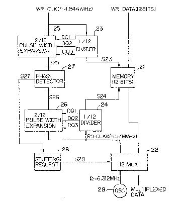
Now, referring to Fig. 7, an embodiment of a
digital data multiple conversion system in accordance
with the present invention will be described.
The digital data m~11tiple conversion system shown
in Fig. 7 is able to multiple-convert data of the first
order group and having the frequency ~1 = 1.544 MHz into
data of the second order group and having the frequency
f2 = 6.312 MHz . The digital data multiple conversion
system further includes a first pulse width expansion
circuit 25 and a second pulse width expansion circuit 26
in addition to the circuits 21, 22, 23, 24, 27, 28,
and 29 of the digital data multiple conversion system
shown in Fig. 2~
Figure 8 shows a circuit diagram of a 1/12
frequency divider circuit which can be applied to the
first and second frequency dividers 23 and 24. The 1/12
frequency divider circuit shown in Fig. 18 includes 12
series-connected delay-type flip-flops (D-FFs~ DFFl to
DFF12 and a NAND gate NANDl. The 1/12 frequency divider
circuit shown in Fig. 8 is formed as a ring counter.
Figures 9a to 9m show timing charts of the 1/12 frequency
divider circuit shown in Fig. 8.
The first 1/12 frequency divider circuit 23 receives
the write clock WR-CLK of the frequency fl = 1.544 MHz,
and outputs 12 frequency-divided pulses DQl to DQ12 as
the first frequency-divided signal S23. The second 1/12
frequency divider circuit 24 also receives the read
clock RD-CLK of the frequency f1' = 1.574 MHz from the
12 multiplexer 22, and outputs 12 frequency-divided
-- 10 --
pulses DQl to DQ12 as the second frequency-divided
signal S24. In the above, the number 12 corresponds to
the bit length 12 of the write data WR-DATA and the read
data RD-DATA~
Figure 10 shows a circuit diagram of the memory 21.
The memory 21 includes 12 parallel-connected D-FFs 21
to 21A12 , 12 parallel-connected NAND gates 21Bl ~o
21B12 , and a ~AND gate 21C. The memory 21 receives the
serial write data WR-DATA, and stores the same to the
parallel-connected DFFs 21Al to 21A12 in response to the
12 frequency-aivided pulse train DQ1 to DQ12 as the
first frequency-divided signal S23. Thus, the data
stored in the DFFs 21Al to 21A12 is parallel data. The
stored data in the DFFs 21Al to 21A12 is output to the
NAND ~ate 21C in response to the 12 frequency-divided
pulse train DQl to DQ12 as the second frequency-divided
signal S24. The read data RD-DATA output from the ~AND
gate 21C is serial data.
Figure 11 shows the pulse width expansion
circuit 25. The pulse width expansion circuit 27
includes an OR gate 251 and a DFF 252. The OR gate 27
receives the first and second frequency divided pulses
DQl and DQ2 of the first frequency-divided signal S23
from the first frequency divider circuit 23. The
DFF 252 receives an output of the OR gate 251 at a delay
input terminal D and is turne~ O~ in response to the
write clock WR-CLK. A positive output of the DFF 252 is
supplied to the phase detection circuit 27. The DFF 252
is cleared by the third frequency-divided pulse DQ3 of
the first frequency-divided signal S23. As a result,
the pulse width expanded signal S25 has two pulse widths
of a pulse width of the frequency divided pulse.
Figures 12a to 12c show the generation of the pulse
width expanded signal S25.
In this example, the pulse width expansion
circuit 25 recovers a loss of a single pulse of the
write clock ~R-CLX.
~353a~0
In this example, the consecutive frequency-divided
pulses DQl to DQ2 are used for recovering the loss of a
single pulse of the write clock WR-CLK except for the
frequency-divided pulse DQ3 using the reset of the
DFF 252. In general, m consecutive frequency-divided
pulses are required for recovering a loss of an Im-l)
pulse of the write clock WR-CLK, m consecutive frequency-
divided pulses can be replaced at least start and end
frequency-divided pulses, a number of pulses therebetween
corresponding m.
The second pulse width expansion circuit 26 can be
formed in the same way as the first pulse width
expansion circuit 25.
Figure 13 shows a circuit diagram of the phase
detection circuit 27, the stuffing request circuit 28,
and a part of the 12 multiplexer 22. The phase detec-
tion circuit 27 comprises a NAND gate 27A and receives
the first and second pulse width expanded signals S25
and S26, and outputs a low level phase detection
signal S27 when both of the received pulse expanded
signals S25 and S26 are high level. The pulse width of
the phase detection signal S27 is an overlapped ON time
of the first and second pulse width expansion
signals S25 and S26. The stuffing request circuit 28
comprises two NAND gates 281 and 282 to form a latch
circuit, and outputs the low level stuffing request
signal S28 when the phase detection signal S27 is input.
The 12 multiplexer 22 includes a flip-flop 22A, for
latching the stuffing request signal S28. Upon receipt
of the stuffing request, the stuffing request circuit 28
and the flip-flop 22A are reset by supplying a reset
pulse RESET from the 12 multiplexer 22.
Now, the operation of the digital data multiple
conversion system shown in Fig. 7 will be described with
reference to Figs. 14a to 14f and Figs. 15a to 15f.
In Fig. 14a, the write clock WR-CLK is lost at a
time tl. However, the pulse width expansion signal S25
;3~
- 12
has two pulse widths of a single write clock WR~CLK, and
as a result, a phase matching between the pulse width
expansion signals S25 and S26 is obtained at the phase
detection circuit 27, and the stuffing request signal S28
is issued from the stuffing request circuit 28. The 12
multiplexer 22 carries out the stuffing of the read
clock WD-CLK at a time t3, regardless of the loss of the
read clock WD-CLK at a time t2.
In Fig. l5a, a single pulse of the write clock
WR-CLK is lost at a time tll. In Fig. 15c, a single
pulse of the read clock RD-CLX is lost at a time tl2.
These lost pulses lay between adjacent pulse width
expansion signals S25, but the number of lost pulses is
the same, and thus a normal operation is carried out.
As described above, the digital data multiple
conversion system shown in Fig. 7 carries out a normal
data multiplexing regardless of the loss of a single
pulse of the write data WR-DATA and/or a single pulse of
the read data RD-DATA. In addition, the pulse width
expansion circuits 25 and 26 are formed by a simple
circuit, as shown in Fig. 11.
Figure 16 shows another circuit diagram of the
phase detection circuit 27 and the stuffing request
circuit 28. The phase detection circuit 27 comprises a
NAND gate 27B, and the stuffing request circuit 28
comprises a resister 285 , a capacitor 286 ~ and an
inverter 287. The resister 285 and the capacitor 286
form a time constant circuit; the time constant thereof
being shorter than a period o~ the frequency-divided
signal S23. This analog-type stuffing request
circuit 28 ~oes not require the reset pulse RESET from
the 12 multiplexer, as shown in Fig. 13.
Figure 17 shows a circuit diagram of a general
digital data multiple conversion system. In Fig. li,
reference N indicates a bit length of an input data
IN-DATA and an output data OUT-DATA and a frequency
dividing factor, and m and n denote pulse widths to be
3~3
expanded. If the number of lost pulses of an input clock
IN-CLK is one, _ is two. Similarly, if the number of
lost pulses of the read clock RD-CLK is one, n is two.
The digital data multiple conversion system of
Fig. 17 can be applied to any portion in the digital
data communication network.
Also, the digital data multiple conversion system
of Fig. 17 can be applied to a digital data de~ultiple
conversion system by replacing a demultiplexer (not
shown) with the multiplexer 22, since the data write at
one frequency and the data read at another frequency
different to the fixst frequency are xequired in the
data demultiplexing, and in the demultiplexing, the
above lost pulse may be recovered.
Many widely different embodiments of the present
invention may be constructed without departing from the
spirit and scope of the present invention, and it should
be understood that the present invention is not
restricted to the specific embodiments desc~ibed above,
except as defined in the appended claims.