Note : Les descriptions sont présentées dans la langue officielle dans laquelle elles ont été soumises.
~.28636~
IN-PLACE DIAGNOSABLE ELECIRONIC CIRCUIT BOARD
Back~round of the Invention
This invention relates to fault diagnosdcs in electronic circuits. More
particularly, this invention relates to methods and arrangements for communicating
5 fault diagnostics to repair systems.
VLSI technology pe~nits fairly complex subsystems to be packaged
on removable, or pluggable, circuit packs. The cost of a circuit board increaseswith complexity, and complexity increases with advances in VLSI manufacturing
technologies.
High circuit board costs make repair of failed circuit boards desirable,
but the complexity that comes with VLSI makes field repair almost impossible.
Consequently, many current system designs incorporate methods and hardware
means for isolating faults to revable sub-assembly (e.g., a circuit board), andrdy on a field technician to locate the failed sub-assemblies, replace them, and15 send the failed units to repair centers.
In some software-based systems, diagnostic software is also
incorporated which is ~ctivated either automatically, or manually, and that
software exercises the system and locates the faults to within the desired
granularity. Typically, the desired granularity is the removable circuit board. In
20 most of these applications, detailed diagnostic results are summarized into apass/fail indication, and the indication is presented to the repair technician so that
proper circuit board replacements can be effected. A failed circuit board is then
removed and returned to the factory for repair, often with a written summary of
the indications presented to the technician.
A number of limitadons exist with the present techniques. First,
detailed test results are not reliably and accurately returned with the circuit boards
to the repair center. This relates to the practical problems of recording test
indicadons accurately, loss or separation of thc diagnosdc record dur~ng transit of
the failed circuit board, etc. Second, once the failed circuit board arrives at the
30 repair center, repair must begin with thc minimal information provided about the
latest circuit board failure. Third, to proceed with repair, external equipment is
requircd to invoke testing and obtain results, and there is some question whether
thc original failurc can be induced again and identified.
Summary of the Invention
In accordance with the principles of this invention, an on-board self
diagnostic capability is realized in a circuit board with a microprocessor which is
located on the circuit board and which interacts for diagnostic purposes with the
: . :
.: -
.
,
.
363~i~
.,
functional circultry on the board. The microprocessor
interacts with an electrically erasable read-only-memory
(EEROM) that is also located on the circuit board. Diagnostic
signals occurring during the circuit board's normal operation
are automatically detected and stored in the EE~OM.
Additionally, a control port at the circuit board permits
activation in the microprocessor of diagnostic routines that
accept input test data, apply test sequences to the functional
circuitry and store the diagnostic results in the EEROM.
Also, through control of the microprocessor, the EEROM is
accessed to retrieve previously stored diagnostic results.
In accordance with one aspect of the invention there
is provided a circuit assembly for performing a preselected
function comprising first means for performing said
preselected function; second means, responsive to an applied
stimulus, for developing a test sequence and applying said
test sequence to said first means; and robust memory means for
storing selected signals of said first means that occur in
response to said test sequence.
In accordance with another aspect of the invention
there is provided a method for failure tagging of a removable
electronic sub-assembly containing functional circuitry, means
for testing said functional circuitry and a robust memory
responsive to said means for testing for storing results
obtained by said means for testing, comprising the steps of:
detecting conditions in said functional circuitry that merit
storing; and storing said conditions in said robust memory.
Brief Des¢ription of the Drawinq
FIG. 1 illustrates a block diagram of circuitry on a
pluggable board that affords the in situ diagnostics
capabilities of this invention;
FIG. 2 presents a flow chart of the major processes
in the microprocessor of FIG. l; and
FIG. 3 presents a flow chart of operational
sequences related to the maintenance of the pluggable circuit
board.
-:
128636~
Detailed DescriPtion
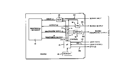
FIG. 1 depicts one realization of a plug-in board
design in conformance with the principles of my invention.
The primary elements in the FIG. 1 board design are the
functional circuitry, 10, the on-board microprocessor, 20, and
the on-board electrically erasable memory (EEROM), 30. The
functional circuitry performs whatever function is desired of
the board, and interfaces with the other elements or
subsystems outside the board via board input leads 101 and
10 board output leads 102. Leads 101 are connected to input
leads 11 of circuitry 10 by way of two-input multiplexer 40,
while leads 102 are connected to output leads 12 of circuitry
10 by way of switch 50. In addition to the functional input
and output lead sets 11 and 12, the FIG. 1 arrangement
includes additional leads going to and from circuitry 10;
specifically, diagnostic input leads 13 and diagnostic output
lead 14. Often, sufficient diagnostic information can be
derived from a circuit simply by observing the signals at the
normal output leads (12) and comparing them to the expected
output signals. In other circuit designs, specific circuitry
is provided for error detection, and the output signals of
those circuits form diagnostic failure tagging outputs which,
for example, trigger an alarm. In still other circuit
designs, the electrical signals at various intermediate points
within circuitry 10 may be particularly useful in pin-pointing
failed components or subsystems, and those intermediate points
are brought out through additional diagnostic output leads.
It is the collection of these diagnostic leads that
.,
~'. - ~ .'' ' . ,:
.
i286~6~
comprises leads 14 in FIG. 1, and those leads combine with output leads 12 to
form data bus 16. Data bus 16 is applied to microprocessor 20 and to EEROM
30.
The expected output signals on bus 16 relate, of course, to the input
5 signals applied to circuitry 10. In most designs, however, passive observation of
the output signals is not sufficient to detect the occurrence of all possible
malfunetions; and even if it were sufficient, detection of errors merely by
observing output signals in response to the normally applied input signals wouldrequire microprocessor 20 to have very extensive computing and/or storage
10 capabilities. Artisans generally overcome this problem by specifying vanous sets
of diagnostic input signal sequences that "exercise" the circuitry in a
predetermined manner and thereby uncover malfunctions efSciently. It is for thispurpose that multiplexer 40 is included.
In FIG. 1, diagnostic sequences can be applied to circuitry 10 via
lS input leads 11 or via diagnosdc input leads 13. Input leads 11 receive signals
dther fiom bus 101 or from bus 15 (depending on the state of multiplexer 40),
whereas diagnosde input leads 13 recdve signals only from bus lS.
Wbile diagnosde routines are bein8 ca~ied out, it may be desirable to
not provide output signals at output leads 12. It is for this purpose that switch 50
20 is provided. Both muldplexer 40 and switch 50 are controlled by microprocessor
20, via eontrol bus 17.
To maintain a history of the diagnosde outputs, FIG. 1 provides for
the storage of the diagnosde output signals of bus 16 in EEROM 30, in addidon
to these diagnosde signals being provided to micropmcessor 20. EEROM 30 is a
25 convendonal, commercially available, unit. W iting into, and reading from
EEROM 30 is controlled by microprocessor 20.
Mieroprocessor 20 is a convendonal microprocessor with an
associated memory 60 wbich comprises a read-only pordon and a read-write
portion, In FIG. 1, microproeessor 20 has a user data input 104, a user control
30 input 10S and a status indication ou~put 106. Status indicadon output 106 may be
a multi-lead output that provides information to the system outside the board
coneerning tho operatdonal well-being, or state of the functdonal cireuitry and of
tho mieroproeesso~. Ussr eontrol input 10S p~rmits the system outside the board
to inid~ seleeted routines to be performed by microprocessor 20 while user data
35 input 104 permits data to be hjeeted into microp~cessor 20. Injecdon of data
into mieroproeessor 20 may be useful h some of the diagnosdc roudnes because
it ean initiats various registers, sst different thresholds, and place the functional
. ... . . . . . . . .. .
.. . ,. ~ .. .
.~ , .. .. . .
., . , . . . . - .. . -
'' ' ' ' ' - . -
.~ . .
; . . .
i~28636~
circuitry at any preselected state via buses 11 and 13. Being able to preset
circuitry 10 to a preselected state substantially speeds up the diagnostic process.
As an aside, the specific state applied to the functional circuitry 10 can also be
obtained from memory 60 into which data may have been placed either by the
5 designer (into the ROM portion) or by the capturing of a previous state of the system in the read-write portion of the memory.
Inputs 104 and 105 provide information to microprocessor 20 from
the system outside the board. Bus 16, on the other hand, provides information tomicroprocessor 20 from within the board. As described above, bus 16 contains
10 the normal output leads and the diagnosdc output leads of circuitry 10.
Consequently, microprocessor 20 can initiate diagnostic routines automatically in
response to various preassigned states on bus 16, or following an analysis of
signal sequences on bus 16 which may indicate the need for diagnostics. Based
on its various inputs, microprocessor 20 also selects the outputs on bus 16 that are
lS to be stored in EEROM 30.
PIG. 2 presents a flow diagram depicting the operation of
microprocessor 20. Following START block 200, initializations are perforrned in
block 220, and control passes to decision b1Ock 201, where a deterrnination is
made conceming the status on bus 16. When bus 16 indicates that a fault exists or
20 that a potential fault may exist, control passes to path 202, the fault indication is
recorded in EEROM 30 (block 203), and microprocessor 20 proceeds to ascertain
the kind of action that is required in response to detected fault or potential fault
(block 204). Sometimes the failure is not catastrophic and the design of the
functlonal circuitry can compensate for the failure. In such cases, merely
25 recording information conceming the failure (failure tagging) is sufficient. When
no addidonal action is required (other than recording the fault) decision block 205
passes control back to decision block 201. When i~ is ascertained that a
diagnosdc routine is to be inidated, control passes to block 206.
When no faults are detected on bus 16 by decision block 201, control
30 passes to decision block 207 where attention is directed to input 105. When input
105 does not request the initiadon of diagnostic routines or outputting of data
stored in EEROM 30, an "all is well" output is delivered to output leads 106
(Uock 208) and control retums to decision block 201. When input 105 does
request the initiation of some routine, contro1 again passes to block 206.
Block 206 is reached whenever a routine needs to be executed by
microprocessor 20. The input requesting the diagnosdcs (be it input leads 105 orbus 16) also provides an indicadon as to the particular diagnostdc routine that
.
: . .. . .
.
'
.
: '
~8636~
ought to be exercised. The selection of the diagnosdc roudne and the running of
same is performed in block 206, with the results of the roudne being recorded inEEROM 30 (block 209), if called for. Decision block 210 ascertains whether the
encountered fault or the diagnosdc results indicate that the subject board should be
S redred from service. When such is not the case, control returns to decision
block 201. Otherwise, an alarm is presented to output 106 (Uock 211) and the
microprocessor's operations are terminated by END block 212. When that
happens, the failed board is removed from service and sent to the repair center.As depicted in FIG. 3, in the repair center, the contents of EEROM 30
10 are accessed via control of microprocessor 20. Leads 104, 105 and 106 permit
activating the r~croprocessor's routines, the routine can output the contents ofEEROM 30 (block 302) and can exercise the funcdonal circui~y with additional
test sequences (block 304). With the aid of the available informadon the board
can, hopefully, be rep~ured and forwarded for new service (block 305). Of course,
15 as part of thc repair, thc EEROM would be erased in the manner specified by the
EEROM's manufacturer.
The versatility of the structure depicted in FIG. 1 can be appreciated
from a number of the very desirable features that I have implemented with this
structure. One feature, for example, is a routine embedded in microprocessor 20
20 that detccts the initiation of opcratdons (e.g., when power is turned on). That
routine is pcrformed in block 220. Block 220 also inidalizes or configures the
functional circuitry in accordance, for cxamplc, with thc functdon that it must
pcrform bascd on the specific locadon whcre it is inserted within the overall
systcm. For instancc, funcdonal circuitry 10 may be a muld-pole Bessel filter,
25 with the number of reaL;zed poles bcing controlled by microprocessor 20. In one
locadon within the ovcrall system, inputs 105 may specify a three pole realizadon,
while at another location within the overall system, inputs 105 may specify a four
pole realizadon. Such reconfiguring is easily accomplished within the roudnes ofbloclc 220.
Another feature, for examplc, is a storagc intcgrity chcck. Sincc one
of the primary bcncfits of my invendon is thc availability of stored diagnosdc
infonnation, it is cssentdal to protcct this asset. The quesdon arises, then, of what
happcns when EEROM 30 fails eithcr partially or completely. Clearly there must
be a procedurc included that vcrifies the storage of informadon. In accordance
35 with one aspect of my invention, each wridng of data into EEROM 30 (e.g. in
block 209) is effected by microprocessor 20 with a roudne that reads the contents
of EEROM 30 in thc stored locadons and compares that which has been stored
: '.' ' : ' '
. . ' , .
,
.
,
- 6 -
12~3636
with the informadon of which microprocessor 20 is aware. When the information
storage is successful, there is a match and the routine exits normally. When there
is no match, the routine tries to read again and, failing to successfully accomplish
that task, the data is read into a different portion, or block, of EEROM 30. The5 rationale for that is the hope that the failure of EEROM 30 is only partial and
that, therefore, the diagnostic information can still be saved.
The descriptions presented herein are illustrative of the principles of
my invention, and it should be understood that variations in construction and
embodiment can easily be incorporated in the FIG. 1 design without depardng
10 from the spirit and scope of this invention. For example, the disclosure herein
describes the use of an electrically erasable read-only-mery (EEROM 30). The
aspect of this memory that is critical to its operations in the context of this
invention is its "read-only" feature, or, more specifically, the feahlre of read-only
memories where contents of the memories remain unaltered by the removal of
15 power. The erasable read-only-memory has the advantage of being reusable, butthat is not critical. In appropriate circumstances, it may be economically feasible
to employ a different memory that maintains its contents in the absence of power,
or even to employ a conventional read-only memory (ROM) that may be written
into by microprocessor 20 only once. After use at the repair center that ROM
20 may be reved and replaced with another one. In the context of this disclosure,
all versions of memory that can be used in the FIG. 1 arrangement and maintain
their contents (without power external to the board) for a period of time that is
sufficient to bring the board to a repair center and read the memory's contents,shall bc encompassed by thc tcrrn "robust mcmories".
. - '
,
.
.
,
,~.~, ~ '' ' ' ,