Note : Les descriptions sont présentées dans la langue officielle dans laquelle elles ont été soumises.
735
CASCADED INTERNAL IMPEDANCE DEPENDENT
AMPLIFIER WITH ACCURATE VARIABLE GAIN CONTROL
1 BAcKGRouN--n OF THE INVENTION
1. Field of the Invention
The invention relates to the ~ield of analog
circuit desiqn and in particular relates to the desiqn
S of cascaded amplifiers wherein temperature independence
and accurate qain control is provided.
2. Description of Related Art
: ___ _ _ _ . ~. A. . _ __ __
In certain types of app]ications accurate ~ain
control in portions of the electronic circuitrY is
essential to the ef~ective or use~ul functionin~ of
the system. One such class of systems include radar
systems, particularly those radar systems which require
multiple channels and accurate equal ~ain control.
In the prior art, gain adjustments in amplifiers
in radar systems were made usinq a delta qain control
AGC circuit for multiple channels o~ the amplifier.
However, even where each channel is separately adjuste~,
the relative gain amon~ channels must not only be
initially calibrateA or equalized, but ~uch equalization
must be maintainefl over time as wellO Therefore the
prior practice has been to provide an aAditional delta
gain control AGC circuit to compensate or drifts in
3~i
1 gain among the various channels of a multiP1e channel
amplifier. Nevertheless, such prior art desiqns require
periodic checking to match the gain of the multiple
channels.
In addition prior art circuits which incorporate
some type of gain reduction inherently, by virtue of
their design, affect the noise figure of the amplifier,
namely the hi~her the qain reduction the hiqher the
noise figure. Similarly, the gain of such prior art
circuits may become non-linear at hi~h gain reduction.
What is needed then is a design for an amplifier
which includes an accurate qain control which is of
such a design that:
(a) the need for periodic checking, particularly
in a multiple channel amplifier is eliminated, and (b)
the gain does not lose linearity or suffer a deterioration
of its noise figure with hi~her qain reduction.
SUMMARY OF THE INVENTION
The invention is an internal impedance dependent
amplifier circuit which is characterized by an
amplification gain according to an impedance at a
predetermined node of the amplifier, and which is
characterized by an accurate qain control (hereinafter
termed "AGC") achieved by accurately controllin~ the
internal impedance of the amplifier. ~y reason of this
combination the ~ain of the amplifier circuit is
selectively determined. The AGC circuit comprises in
turn a diode and another subcircuit for applyinq a
forward bias current to the diode to vary its impedance.
The AGC circuit provides a log linear impedance with
respect to a selective control si~nal applied thereto.
A log linear impedance is defined for the purposes of
this specification to mean an impedance such that if
the logarithm of the qain of the AGC is linearly varied,
the logarithm of the imPedance will also vary linearlv.
3~
1 In particular, the AGC circuit is a PIN diode and the
selective control siqna] is a forward biased current
applied thereto.
Amonq the advantaqes of this circuit is the
surprisinq result that the noise fi~ure of the amplifier
is affected only to a very minor extent by the maqnitude
of the AGC control siqnal. Moreover, the linearitY of
the amplifier is not only retained at hiqher qain
reduction maqnitudes, but actually improves with hiqher
gain reduction ma~nitudes.
In addition the subcircuit comprises a temperature
compensation subcircuit for driving the diode forward
biased current independently of thermal parametric
variations of the diode. In more qeneral terms, the
AGC circuit further comprises a temperature indePendent
subcircuit for drivinq the AGC circuit independently of
thermal parametric variations of the AGC circuit.
The invention further comprises a plurality o~
impedance controlled amplifiers and correspondinq AGC
subcircuits. Each imPedance controlled amplifier has
an input and an output node. The output node of each
impedance controlled amplifier is coupled to the input
of another one of the plurality of impedance controlled
amplifiers to form a cascaded series of the plurality
of impedance controlled amplifers. One of the Plurality
of impedance controlled amplifiers has an input port
and the last one of the plurality of impedance controlled
amplifiers has an output port to provide an input and
output of the cascaded series of impedance controlled
amplifiers respectively. The cascaded plurality o~
amplifiers is also characterizsd by a loq linear qain
with respect to the AGC voltaqe. The loq linear relation
of gain to AGC control voltaq~ is achieved by providinq
each correspondinq AGC circuit of the pluralitv of
impedance controlled amplifiers with a common AGC
control voltaqe.
, ~ ~ ;
`` ~2~35
1 The invention further includes a plurality of
impedance controlled amplifiers coupled to form a
subplurality of cascaded series connected impedance
controlled amplifiers. Each one of the subplurality of
cascaded series connected impedance controlled amPlifiers
defines a separate channel havina a correspondinq
separate input and output.
In more specific terms the invention is an amplifier
circuit comprising a first active stage, which is a
voltage amplifier; a second active stage, which is a
current amplifier, havinq an input coupled to the first
stage; and a subcircuit for providin~ a gain control which
couples to the node between two stages. The subcircuit is
independently driven with respect to the first and second
staqes. The subcircuit provides a log linear feedback
signal to drive the internal loading impedance of the
first staqe. In particular the subcircuit ComPrises a
PIN diode selectively driven by a forward hiased current
to vary the impedance of the PIN diode in the amplifier
comprised of the first and second stages. The first
stage of the amplifier is a common base transistor and
the second staqe is an emitter follower transistor. The
PIN diode is coupled to the node between the output of
the common base transistor and the input of the emitter
follower transistor. The suhcircuit comprises another
or second PIN diode to compensate for temperature drift
of the PIN diode, which second PIN diode is selectively
driven hy a forward biased current to vary the impedance
of the PIN diode in the amplifier.
The invention also includes a method for control]inq
the gain of an impedance controlled amplifier comPrisinq
the steps of couplinq a variable resistance to a pre-
determined node within the impedance controlled amplifier,
the impedance controlled amplifier beinq characterized by
3~
having a gain determined by the impedance at the
predetermined node, and the step of varying the variable
resistance coupled to the node in a log linear fashion. In
the step of varying the variable resistance, the forward
biased resistance of a PIN diode is coupled to the
predetermined node by varying a forward biased current
applied to the PIN diode. The method further comprises the
step of varying the forward biased current in the PIN diode
in a temperature compensated manner.
The method still further comprises the steps of coupling
and varying the forward biased current in the PIN diode in a
plurality of cascaded impedance controlled amplifiers, each
amplifier being controlled by a common voltage.
Other aspects of this invention are as follows:
An amplifier circuit comprising:
a first active stage;
a second active stage having an input coupled to said
first stage; and
means for providing a feedback signal to said first
stage, said means being independently driven with respect to
said first and second stages, said means providing a log
linear feedback signal to said first stage.
A method for controlling the gain of an impedance
controlled amplifier comprising the steps of:
coupling a variable resistance to a predetermined node
within said impedance controlled amplifier being
characterized by having a gain determined by the impedance at
said predetermined node; and
varying said variable resistance coupled to said node in
a log linear fashion.
An amplifier circuit comprising:
a first active stage comprising a common base transistor
having an output;
a second active stage comprising an emitter follower
transistor having an input coupled to the output of said
first active stage;
a PIN diode which is independently driven with respect
,~
7~5
5a
to the firs~ active and second active stages by a forward
biased current ~o vary the impedance of said PIN diode and
theraby provide a log linear signal to said first active
stage; and
one terminal of said PIN diode being coupled ko the
output of said first active stage and to the input of said
second active stage and the other terminal of said PIN diode
being coupled to ground.
BRIEF DESCRIPTION OF THE DRAWINGS
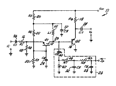
Fig. 1 is a schematic diagram of an intermediate
frequency (IF) single stage amplifier incorporating the
invention.
Fig. 2 is a schematic diagram of a temperature
compensation subcircuit used in combination with portions of
the circuitry of Fig. 1.
Fig. 3 is a blocX diagram of a plurality of amplifiers
as described in connection with Figs. 1 and 2 shown as
serially cascaded.
DESCRIPTION OF THE PREFERRED EMBODIMENTS
An internal impedance dependent amplifier has a gain as
determined by the impedance at a predetermined node within
the amplifier. A PIN diode is coupled to the predetermined
node. The PIN diode is driven with a forward biased
current which serves as the accurate gain control (AGC)
signal for the amplifier. In the preferred
~ ,,
s
1 embodiment, the PIN diode is driven by an operational
amplifier in such a manner that the imPedance thus couPled
to the predetermined node in the amplifier is temParature
independent. Because the PIN diode has an impedance
qiven by:
loq R = A + B loq Ip,
where0
R is the impedance of the PIN diode;
Ip the forward biasing current; and
A and B constants which are different for each
PIN diode,
the AGC voltaqe applied to the operational amplifier
drivinq the PIN diode is loq linear with respect to the
impedance of the PIN diode and hence also loq linear
with respect to the voltaqe qain of the impedance
dependent amplifier to which the PIN diode is coupled.
This characteristic of the ~ain of the amplifier allows
the amplifier to be cascaded in series and to preserve
the same impedance relation as expressed above for the
cascaded series of ampli~iers as well. Thus, the
voltaqe ~ain of the cascaded series of amplifiers is
also loq linear with respect to a common AGC voltaqe
applied to each of the amplifiers of the series.
As will be made apparent in the following
description, the noise fiqure of the amplifier or a
cascade of such amplifiers is substantially independent
of the AGC volta~e because ~ain is determined by the
PIN diode's impedance, whose contribution to noise
fiqure is relatively independent of the maqnitude of
the impedance or at worst a very slowly varyinq function
of its impedance.
1 The invention is an amplifier which is temperature
independent and qain trackina by usin~ the radio
frequency (RF) characteristics of a PIN diode. It is
known that the loqarithm of the RF resistance of a PIN
diode is loqarithmically linear with respect to its
forward current~ The amplifier of the Dresent invention
thus has its qain resistively controlled. By usinq a
lo~ linear PIN diode as the qain determininq resistive
element, amplifier qain can then be made lo~ linear
relative to the qain control volta~e. As a result, an
amplifier with a high dynamic ranqe, low intermodulation
distortion and gain control with output noise reduced
proportional to the gain reduction is realized. For
e~ample, using a typical PIN diode in a cascaded
amplifier, gain control accuracy of better than 0.5 dB
over a range of 60 dB with temperature chanqes of more
than 25 degrees C in the temperature ranqe of
-55 degrees C to 85 deqrees C is achieved.
The function of the amplifier qain can be verified
by takin~ input and output readinas at only two points.
This results in considerable ease in ~ain calibration.
Because of the ease in qain calibration, the
design of the amplifier readily allows for adjustments
to be made takinq into account the individual constants
of the operative gain determinin~ element, i.e. the PIN
diode.
As ~ill be ascertainable below, the center
frequency of the amplifier is set by a sinqle inductive
element, which permits a hybrid circuit desi~n of small
size and easily adiustable ~erformance. This makes the
desiqn a universal circuit block usable in a wide variety
of applications with no redesiqn re~uired.
7~3S
1 of particular advantage is the ~act that as the
gain control voltaqe changes in the circuit, the phase
of the center ~requency does not chanqe. This is c]earlY
an advantaqeous attribute where, as in radar circuits,
the phase of a received si~nal carries siqnificant
information. In the prior art, compensation of some
sort was reauired to accommodate phase chan~es in the
center frequency of the tuned amplifiers as qain chanqed.
This is unnecessary in the circuit of the invention.
As will further be described below, as the current
in the PIN diode increases (increasing qain reduction)
the voltage distortion across the PI~ diode decreases.
Thus, unlike prior art amplifiers, the linearity of the
circuit of the invention actually improves with qain
reduction.
Exactly how these advantages are accomplished is
better understood by turnin~ to the schematic dia~ram
of FIG. 1.
The amplifier, generally denoted by reference
numberal 10 is a resistance dePendent amplifier which
forms the core of the lo~ linear ~ain control IF
amplifier. Amplifier 10 is comprised of two active
devices, complementary transistors 12 and 14, and inPut
resistor 16. I~norinq frequency dependence impedances
in FIG. 1 for the moment, disconnectinq suhcircuit 24,
and substitutinq a resistor Rc for it, (which assumes
that Rc is not more than one tenth of the value of the
output impedance of transistor 12 and the input impedance
of transistor 14), and concentrating only on the
transistor parameters and resistances, it can be shown
that the voltage qain of amplifier 10 is approximately
equal to:
__ f~
~3b~5
1 Vo / Vi = Rc / Ri ,
where
Vo is the output ~o.ltaqe;
Vi is the input voltaqe:
Rc is the resistance of node 2h which is
dominated by PIN diode 42;
Ri is the amplifier input resistance.
Hence the qain of the amplifier is the ratio of its
input impedance, Ri, and the im~edance of PIN diode,
Rc. Many of the advanta~es of the circuit desi~n
discussed above result from the dependence of ~ain and
other circuit parameters on the PIN dio~e's impedance
and the inherent properties of the PIN diode. Therefore,
amplifier 10 combines the voltaqe qain of transistor 12
with the current ~ain of transistor 14 to Provide an
overall power ~ain with fixed in~ut and output impedances.
What needs to be particu].arly emphasized here is
that the gain of amplifier 10 is almost entirely
determined by the ratio of a function of the qain control
resistor Rc to the input resistance Ri and less affected
by any transistor parameters than in prior art amplifiers.
Alternatively stated, the ~ain is determined hy the
resistance or impedance at node 2fi.
The lo~ linear ~ain control is effectuated throu~h
a subcircuit, ~enerally denoted by reference numeral 24.
As implied in the above discussion of amplifier 10, the
qain of the amplifier is determined by the RF impedance
at node 26.
2~73~
1(~
1 Capacitors 28-34 are RF ~ecouPlin~ capacitors
used in a conventional sense in amplifier 10 in a manne~
which shall not be further described here. Similarly,
capacitors 36 and 38 are input and output dc blockinq
capacitors respectively which are also conventionallv
employed at the input and output of the sinqle staae
amplifier 10 shown in FIG. 1. Ca~acitor 40 is, however,
an RF coupling capacitor which is used to couple the RF
signal, which is being amplified, to PIN diode 42. It
is well known that the RF resistance of the PIN diode
is given by the following equation:
log R = A + B log Ip
where
R is the RF resistance of PIN diode 42;
A and B are constants which will be determined
by individual diode: and
Ip is the DC forward current of the PIN diode
42.
Therefore, by applying a predetermined voltaqe, - Vc,
to diode 42, the RF resistance can be varied. Resistors
44 and 46 are thus current limiting resistors to define
the maximum forward current applied by Vc to diode 42.
~esistors 18, 20, 22, 48 and 50 are part of the
conventional biasinq network for transistors 12 and 14
while inductor 52 is chosen to set the center frequency
of amplifier 10.
-` ~21~3~73S
11
1 The effective RF resistance at node 26 is thus
controlled by varyin~ the forward current throuqh diode
42. PIN diodes are characterized in ~eneral by havinq
an almost pure resistance at ~F fre~uencies, whose value
S can be varied from approximately 10 kohm to less than one
ohm by the control current, Ip. Althouqh all diodes show
this behavior to some extent, the PIN diode i.5 o~timize~
to show this characteristic over a wide resistance ranqe,
with ~ood linearity, low distortion and low control
current Arive.
Turn briefly to the schematic dia~ram of FIG. 2.
The PIN diode junction voltaqe chan~es as a function of
temperature. Therefore, it is difficult to control the
~ain control current, Ip, accurately if the control
voltage is directly applied to the PIN diode as the
temperature of diode 42 chan~es. To effect such control,
a subcircuit, generally denoted by reference numeral 54
in FIG. 2, is substituted into amplifier 1~ of FIG. 1
in place of subcircuit 24.
The ~ain control volta~e, Vc, is coupled to the
input of an operational amplifier, qenerally denoted by
reference numeral 56. The output of amplifier 56 is a
volta~e, Vo and a qain control current, IP. A resistor 5
serves as a current limitin~ resistor for diode 42. As
before diode 42 is coupled to no~e 26 of amplifier ln by
couplinq capacitor 40. The remaininq portion of amPlifier
10 has been omitted from the simPlified schematic of
FIG. 2 for the purposes of clarity of illustration. It
follows immediately that:
~ 6~
12
1 Ip = -Vc/Ri
where
Ip is the gain control current at the output of
amplifier 56;
Vc is the input gain control voltaqe at the
input of amplifier 56; and
Ri is the input resistance of resistor 6n.
It is important to note that Ip is independent o~ the
DC junction voltage of diode 42. Therefore, when used
in the circuit of FIG. 2, the forward current throuqh
diode 42 will be automatically adiusted to be independent
of the diode's DC junction voltage and therefore
temperature indePendent. If Ip is thus temperature
independent, then in the equation for the dio~e ~F
resistance given above, R will also be temperature
independent. j~
Therefore, what has thus far been described in a
single sta~e, log linear gain controlled, and temperature
independent amplifier. In other words, a temperature
independent, accurate qain control is provided in
amplifier 10 as long as an AGC log linear volta~e, Vc,
is provided to the input of subcircuit 54 of FIG. ~.
The invention is thus summarized as an amplifier
incorporating a PIN diode whose resistance is used to
control the gain of each staqe. The PIN diode is used
in a temperature compensation circuit so that the ~F
resistance of the diode is temperature independent.
Multiple stages of the basic amplifier block are cascaded
to achieve hiqher gains and AGC ranges. FIG. 3 is a
block schematic of a plurality of amPlifiers 70 such as
7~
13
1 described above with each amplifier coupled in series
to comprise a cascade of n amplifiers, Al, A2, A3, ... An.
Each amplifier 70, Ai, is Provided with a common PIN
diode current, Ip, as the AGC signal. Thus, the cascade
of amplifiers can be treated as a sinqle amplifier,
generally denoted by reference numeral 72, with an
input 74, output 76 and AGC control siqnal, Ip. The
lo~ linear characteristic of the PIN diode is used so
that the overall gain of the cascaded staqes in dB can
be expressed as:
Gain in dB = a ~ b ln(-V)
where
V is the channel's AGC voltage commonly
applied to each staqe; and
a and b are constants which can be determined
by calculations based upon the ~easured
output the voltage of each channel at
predetermined AGC volta~es.
Many modifications and alterations may be made by those
havin~ ordinary skill in the art without de~arting from
the spirit and scope of the invention. Therefore, the
illustrated embodiment must be read only as an example
which has been set forth ~or the purposes of cl~rity
and not as a limitation of the invention as defined in
the followinq claims.
CDB:cal
[272-13]