Note : Les descriptions sont présentées dans la langue officielle dans laquelle elles ont été soumises.
lZB6796
DOUBLE WAFER MOATED SIGNAL PROCESSOR
Background of the Invention
The present invention finds application in connection
with thin silicon plates or wafers formed to ~upport a
multiplicity o~ monolithically integrated data proce~sor
circuits. More particularly, the invention is directed to
the production of circuits formed on silicon wa~ers to
include conductive pads or films formed on at least one
edge thereof, with the remaining poxtion of that edge
10 being in~ulated from the silicon material. The wafer~ may
be stacked and adhesively bonded to form a data proce3sor
module that can be bump bonded to an input eource, e.g.,
an infrared detector array, connected to the module along
the edge portions thereof. Conductive pads formed on the
15 edge portions of the wafers opposite to the input ~ource
can be similarly bump bonded to an array of connector
contacts such as a pin grid array or a printed circuit
board. A plurality of modules can be joined together and
interconnected electrically to form an assembly, e.g. an
20 infrared detector processor as~embly.
Though silicon wafer~ formed in accordance with the
present invention may have application in a variety of
different areas, the present invention is described in
connection with the production of modules ~or space-borne
25 infrared detection sy~tem~, wherein particular
requirements with respect to space, size and ability to
operate in extremely low temperature environments present
criteria for which the present invention ha~ particular
advantages. In view of the ~pace and weight limitations
30 imposed on objects designed to be placed in ~pace the.~ is
a particular need to develop processing modules and
connecting devices that can reliably operate without
imposing sub~t~ntial weight or npace penalties on the
payload.
In order to provide accurate detection and resolution
of objects characterized by an infrared ~ignature, it i6
~ILZ86791~
typically necessary to employ detection sy~ems having a
large number of discrete detector elements. The detector
elements are interconnected ~o form a detector array,
which in turn i8 connected to circuitry to allow the array
to "scan" or "stare" over a substantial field of view.
Accordingly, each of the detector elements must be
electrically connected to processing circuitry in a manner
wherein signals from adjacent detector elements may be
saparately detected and processed. Because the detector
10 elements are small and very clo~ely spaced, e.g., .003
inches center to center spacing, the circuitry for
processing signals from the detector elements must conform
to similar size and space limitations. Many conventional
schemes for connecting detector element~ to the processing
lS circuitry are unsuitable to provide the required
isolation, and reliability. Moreover, production
techniques for connecting the individual detector elements
to dedicated processing circuitry are typlcally expensive,
tedious and characterized by a low degree of reliability.
The technique for connecting in~rared detector
elements and the dedicated processing circuitry requires
that the input3 and outputs of the processor circuits be
electrically i~olated. When the proces~or circult~ are
formed on ~tacked silicon wafers, it is nece~sary to
25 isolate the conductive edge portion from the active
circuitry formed on the silicon wafer ~to prevent
undesired communication between the inputs or outputs and
the processor circuit). Previous disclo~ures modify the
vertical edge portions of the semiconductor wafers after
30 the wafer has been fabricated and the plates are cut
therefrom, to form a non-conductive region on the edge~ o~
the finished wafers to provlde thi~ isolation. For
example, U.S. Patent No~ 4,551,629, to Clark, teache~ that
stacked wafer, i.e. silicon integrated circuits, may be
35 connected to a detector array by selectively etching
between metallized edge portions of the semiconductor
,~ .... ~ .... .. .. . .. . . .. .
~2~367~
wafers and then refilling the etch removed material with
an insulator. The technique for selectively etching and
backfilling edge portlons of ~uch small, thin wafers is
tedious, expensive and difficult.
U.S. Patent No. 4,618,763 to Schmitz, assigned to the
common assignee, di~close~ that a wafer construction
formed of epitaxially grown silicon formed on an insulator
sapphire base. The silicon i~ removed from the sapphire
near the edge portion to provide an insulator substrate
10 for isolated conductive film leads. Though feasible, this
cons~ruction utilizes integrated circuit technology that
is less practiced than that of using a bulk silicon
substrate. Additionally, because the sapphire substrate
is harder and more difficult to produce than silicon, it
15 is more difficult to grind the wafer to the required
thinness necessary to form a high density proce~sor
channel module and it is more expensive.
The present invention is directed to a processor
construction particularly suited for high density
20 environmentg, where conductive end and edge portions may
be isolated from the cilicon material by the formation of
insulator moats constructed in the course of the wafer
fabrication process. The insulator moats are formed in
the silicon wa~er which, after appropriate thinning and
25sizing provides the desired insulator ~ubs~rate end and
edge portions of the wafers. Various techniques are
disclosed or forming the insulator moats, and isolatlng
the silicon from adjacent wafer~ in a wafer stack.
The method of forming a multiwa~er integrated circuit
for abutting electrical connection to external electronics
is disclosed. The method comprises forming a plurality of
groove~ in the first surface of each of first and ~econd
wafers. The grooves are filled with a body of insula~ing
35material and joined along the groove surfaces thereof. In
one embodiment active circuitry i8 formed in one of the
~i _.. , .. ~ ,.. ... . .... ..
~ZB679~;
abutting wafer surface~. In another embodiment active
circuitry is formed in a non-abutting surface of one of
the wafers. Conductive leads are applied to the surface
of one of the wafers to be in electrical communication
with the doped regions. At least one of the conductive
leads extends across at least a portion of the grooves.
The wafers are trlmmed in length 80 that the lengthwise
edgeR of the wafers are defined by the grooves and the
butt end of at least one of the conductive leads i8
10 exposed. A layer of conductive material i8 deposited
along the lengthwise edge of the wafers in electrical
communication with the exposed conductive lead to
facilitate communication between the doped regions and
external electronics.
The invention contemplates the use of different
sequences to form the desired con~truction. The body of
insulating material may be deposited as desired within the
construction sequence. The grooves on each of the wafers
may be filled at different times as preferred. Similarly,
20 the sequence of thinning the wafers may be effected as
most convenient to facilitate construction~ In addition,
a further layer of insulating material may be provided
along the mating surface of one or both of the wafers to
further facilitate isolation of the active circuitry.
It is further anticipated that a plurality of such
integrated circuits may be arrayed, e.g. vertically, to
form a composite module or subarray.
Brlef Description of the Dr w ~
Figure lA is an exploded perspective view of an
30 infrared deteation sy~tem formed to include a plurality of
stacked integrated circuits;
Figures 1~, and lC are enlarged sectional views of
Figure lA;
Figure 2 is a top view of an exemplary silicon wafer
35 used to form structures in accordance with the present
invention;
128679~3
Figures 3(A-F) are side view~ illustrating a fir~t
exemplary manner of forming a multiwafer chip in
accordance with the present invention;
Figures 4(A-C) are ~ide views illustrating a ~econd
5 exemplary manner of forming a multiwafer chip in
accordance with the present lnvention;
Figures 5(A-F) are side view illustrating a third
exemplary manner of orming a third multiwafer chlp in
accordance with the present invention;
Figures 6(A-J) are ~ide vlews illustrating a fourth
exemplary manner of forming a multiwAfer chip in
accordance with the pre~nt invention1
Figures 7(A-D) are side views illustrating a first
exemplary manner of forming a single wafer chip in
15 accordance with the pre&ent invention.
Figures 8(A-D) are side views illustrating a second
exemplary manner of forming a single wafer chip in
accordance with the present invention; and
Figures 9(A-D) are side views illustrating a third
20 exemplary manner of forming a single wafer chip in
accordance with the present lnvention.
Detailed Description of the Preferred Embodiment
The detailed description set forth below in
connection with the appended drawings is intended as a
25 description of the presently preferred embodiments of the
invention, and is not intended to represent the only form
in which the present invention may be constructed or
utilized. The description sets forth the functions and
sequence of steps for construction of the invention in
30 connection with the illu~trated embodiments. It is to be
understood, however, that the ~ame, or equivalent
functions and sequences may be accomplished by different
embodiments that are also intended to be encompa~sed
within the spirit and scope of the invention.
86~t7~
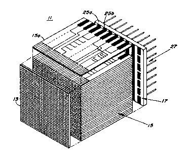
Referring to the drawings, Figure lA illustrates a
perspective view of one application including a plurality
of integrated circuits, stacked to form a module, and
connected to a detector array portion and an output
connector board and pin grid array. As de~cribed ~more
fully below, the integrated circuits may each be formed in
accordance with the present invention. The assembly 11
set forth at Figure lA includes detector array portion 13,
stacked integrated circuit module 15, connector board 17
10 and pin grid array 27. Detector array portion 13 is
typically formed of a large number of individual detector
elements, such as 13a as shown at Figure lB. Module 15 is
formed of a plurality of individual integrated circuit
layers, such as 15a, stacked one atop the next to
15 collectively form the module 15. Each of the layers 15a
is formed to support active circuitry for processing
signals received from detector elements, e.g., detector
for elements in the same horlzontal plane as the layer
15a. Each integrated circuit layer typically includes
20 processing circuitry such that each detector element in a
detector array has a dedicated processor channel.
As shown at Figure lC edge portions of each of the
individual integrated circuit layers, such as layer 15a,
is formed to expose a plurality of input leads or conduits
25 18 which communicate signals from an individual detector
element to a dedicated active circuit portion of the
integrated circuit, i.e. a doped semiconductive region.
The input leads 18 are in electrical communication with
conductive material formed on edge ~urface 19. Edge
30 surface 19 may be provided with a region of conductive
material such as a conductlve pads 22 formed on edge
surface 19 and in electrical communication with leads 18~
Raised sections or bumps 12 are preferably formed on the
outer surface of conductive pads 22 to facilitate
35 connection between the input lead~ 18 and the a~sociated
detector element in detector array 13. Bump~ 12 may be
.. . . . .
67~i
formed of indicium material or the like, applied to the
surface of pads 22 in a conventional manner. Insu1Ator
coat 26 may be provided alony the upper side surface o~
layer 1sa. As further shown at Figure 1s, the detector
array 13 may further be provided with a buffer board 21
used to facilitate electrical connection between the
detector array 13 and the input leads 18. As disclosed
further in U.s. Patent 4,792,672 of December 20, 1988
for Detector Interface Device, assigned to the common
10 assignee, the buffer board 21 may a1BO provide ~dvantage~
in connection with the construction and test~bility of the
detector array 13. As de~cribed more fully below the
pre~ent inven~ion provide~ ~n effective and relia~le
technique for allowlng formation of pad 22 on edge surface
~5 19 of the layer 15a, while isolating the conductive p~d~
22 from the ~illcon 8ub8tr~t~ 23 except through conductlve
leads 18. The present invention permits thi~ isolation to
be effected in the cour~e of fabric~ting the layers 15~
and does not reguire the further proceasing of layers 15a
20 to backfill the in~ulator regions ~nd expo~e leads 18 at
the edge of layers lSaO The invention ~voids the
nece~slty of etchlng edge portion~ of the l~yer 15a ~nd
applying an insulator in the etched regionsO Accordingly
the present invention adv~ntageously eliminate~ tediou~
25 steps as ociated with the manipul~tion of the layex~ after
wafer ~bric~tion.
Connector board 17 i8 prefersbly ~ormed to provide a
plurality of conduc~lve regions 25~, 25b, etc. ~he
conductive region~ are each di~posed in ~butting
30 electrical connection with the layers forming module 15.
~hough not described ~n detail below, lt i8 to be
understood tha~. the principlee of the pre~ent invention
described in connection with electrical communication
between the detector ~rray 13 and the module 15, are
35equally applicable with re~pect to facilitating electrical
communication between the module lS and the connector
~2~6796
-8-
board 17. Pin grid array 27 communicates ~ignals from the
conductive areas 25a, 25b, etc. ~o external circuitry
where furthex processlng occurs.
As generally illustrated at Figure 2 silicvn wafer
31, used to form the integrated circuit layers 15a, may be
constructed to have a plurality of moats or grooves 33
formed in a surface thereof. The moats 33 may be filled
with an in~ulator material in~ulating edge portions of the
chips as described more fully below. By application of
10 the technique~ described below silicon wafer 31 may
produce a plurality of chips~ each defined lengthwise by a
pair of the qroove~ 33 and cut to the de~ired width.
Figure~ 3A-P ~re cros~-sectional view~ illustratlng a
first exemplary manner of forming a chip tlayer 15a) in
15 accordance with the pre~ent invention. Figures 3A-F
illustrate a two wafer method/ of formlng A ~tructure in
accordance with the present inventlon. A~ ~hown ~t Flgure
3A wafers 35 and 37, whlch are typlcally ~lllcon wafers,
are each formed to have grooves 39, 41, 43 and 45 di~po~ed
20 on the oppo~ing surface~ of the wafer3. Th~ groove~ may
be formed by any of a plurality of well known techniques
including ~awing or etching. One of the wafers, e.g.,
wafer 35, may further be provided with an insulating oxide
coating 47 extending along a surface thereof. Grooves 39,
25 41, 43 and 45 may be filled with insulating material,
e.g., silicon dioxide (SiO2) as described more fully
below.
A3 ~hown at Figure 3B wafer portions 35 and 37 may be
joined together along their opposing surfaces. As wafers
30 35 and 37 ~re ~oined groove~ 39, 41, 45 and 43, now filed
with in~ulating material, are placed in abutting
relationship to collectively form moats 42 and 44. As
shown in Figure 3C the top portion of wafer 35 is removed
such that the silicon material 30 forming the principal
35 portion of wafer 35, is bounded by insulating moats 42 and
44 and in~ulator layer 47, which i~ typically SiO2
~LZ~67~36
As shown in Figure 3D active integrated circuitry is
ormed upon the surface of wafer portion 35 by the
formation of doped regions 46~ The doped regions 46 may
be formed in accordance with conventional techniques for
5 forming monolithic integrated circuitry in a
semiconductive substrate. A pattern of conductive leads,
48 provides interconnection between doped regions 46, and
extends across the moats 42 an 44. Conductive leads 48
may be formed of metal, polysilicon or other similarly
10 conductive material. The input leads 18 and output leads
16 are disposed to be in electrical communication with
active circuitry 46, extending over and beyond the
insulating moat~ 42 and 44. An insulator coat 52 i8
provided on the upper surface of conductive portion 45.
15 The insulator coat 52 may be formed of any of a number of
well known in~ulating materials such as silicon dioxide or
silicon nitride.
As shown in Figure 3E silicon i~ then removed from
the wafer 37, e.g. by grinding or lapping, to the required
20 chip thicknegs. Enough silicon is removed such that the
moats 42 and 44 extend to ~he lower surface of wafer 37.
As shown at Figure 3F, chip3 20 or layers 15a are formed
by cutting or sawing through the wafer across the moats 42
and 44. Except for lead~ 16 and 18, extending over moats
25 42 and 44, circuitry 46 is isolated from all other edge
portions of the resulting composite chip 20.
Consequently, the circuitry 46 is isolated from electrical
communication with any other circuit except via edge
portions 49 and 51 of lead~ 16 and 18, respectively. Edge
30 surfaces of the wafer may then be metalized, as shown at
Figure lD to facilitate input to or output from the
circuitry via leads 16 an 18. No etching, filling or
other i~olation techniques need be implemented to isolate
the active circuitrv from the input/output connectors.
As a con~equence of the pre~ent invention multiple
composite chip~ 20 may be adhesively stacked and connected
1~67g~
--10--
to a detector array with fully isolated or insulated
connections. Because the ~ilicon body 35 i8 l~olated from
edge portion~ by mo~t~ 42 and 44 the lnput ~nd output
signals from the chip cannot be co~nunicated to circuitry
46 except via connections to edge portions 49 and 51 of
input and output leads 16 and 18. Accordingly, end
portions of the composite chip 20 are i~olated from the
active circuitry 46 during the wafer fabrication process,
i.e., by forming insulating moats 42 and 44, and by sizing
10 the chip such that the moats 42 and 44 define the length
of the chip. The upper ~urface of the chip 20 i~ isolated
from the surrounding environment by means of in~ulator
coat 52 or by the insulating adhesive used to stack chips
20. The silicon body 30 is further isolated from the
lS lower silicon portion 37 of chip 20 by means of the
insulating oxide layer 47. As described more fully below
the invention may be con~tructed of one layer with the
insulation provided insulator coat 52 on the top of the
chip or by the insulator stack adhe~ive.
In the alternate construction illustrated at Figure
4A, 4B and 4C the composite chip 40 iB formed similar to
the construction described above, except that insulating
material is not deposited in grooves 43 and 45 of wafer 37
prior to joining wafers 35 and 37. Instead, after the
25 composite chip has been trimmed to the required thickness,
exposing grooves 43 and 45 they are filled with an
insulating material, e.g., a glass or resin. A~ shown at
Figure 4C the resulting chip, after trimming the
longitudinal edge~, includes grooves 43 and 45 filled with
30 insulator and grooves 39 and 41 having a body of silicon It
dioxide disposed therein.
Figures 5A, 5B and 5C illustrate another emodiment
wherein the grooves are filled with glass or resin.
Grooves 43, 45 are formed in the surface of wafer portion
35 37. The grooves 39, 41 are coated with a layer of
insulat1ng m~ter1al, 1.e., s111~on dloxide, whlch extends
. ... .. . .
128~7~i
as layer 47 across the surface of wafer 35. Layer 47
coats the interior of grooves 39 and 41. After the wafer
portion 37 is thinned to the required thicknes~, as shown
at Figure SC, the grooves 39, 41, 43 and 45 are filled
5 with insulator material, e.g., glass or re~in a6 shown at
Figure 5D. The application of conductive leads 16, 18,
48, insulating layer 52 and the trimming are illustrated
at Figures 5E and SF, and proceed a~ described above.
Figure~ 6A-J illustrate ~nother lnsul~ted ~ub~trate
lOconstruction wherein the active circuitry is ~andwiched
between the two silicon bodie~. Parallel grove~ 43 and 45
are sawed in wafer 37 as shown at Figure 6A. Active
circuitry 46 i~ formed in the wafer and the wa~er ~urface
i8 coated with oxide 47a as ~hown at Figure~ 6B. Groves
1543 and 45 are gla~s or resln filled afl ~hown at Figure 6C.
Metal leads 16, 18, 48 are formed a~ shown at Figure 6D.
The layer 47a is selectively removed where the conductive
leads 16, 18 and 48 are intended to contact the active
circuitry 46. A second silicon wafer 35 with grooves 39
20and 41 and oxide coat 47B is prepared a~ shown at Figure
6E. A resin adhesive coat 55 applied to the upper surface
of wafer 37 i~ also shown at Figure 6E. The two wafers 35
and 37 are then adhesively bonded as shown at Figure 6F.
Wafer 35 is then thinned to expose grooves 39 and 41 as
25shown at Figure 6G. The groove~ 39 and 41 are resin
filled as shown at Figure 6H. Wafer 37 is thinned to
expose moats 43 and 45 as shown at Figure 6I. Chips are
then sawed from the compo3ite wafer to obtain chips with
the structure a~ described above. Thlfl in~ulated
30substrate or two-wafer embodiment should result in a
higher wafer fabrication yield since the circuit is formed
and all high temperature processes are completed before
the wafers are bonded and thinned. Further, since the
grooves in either wafer can be made relatively deep, wafer
35thinning to expose the moats i~ less critical than in
previously described composite substrate embodiment~.
.. .. . . ... . . . .
lZlY6~96
-12-
Each of the embodiments ~et forth in connectian with
Figures 3-6 has employed a technology utilizing a pair of
semiconductive silicon wafers mated toyether to form a
composite wafer. It is to be understood, however, that
5 the features and advantages of the present invention may
be obtained utilizing a single wafer construction. As
described in connection with the remaining figures a
single wafer may be provided with insulating moats to
insulated edge portions of the chip, and upper insulating
101ayers to insulate the top and portion of the chip. The
insulating moats may be formed to have an oxide filling,
such as silicon dioxide, or may be provided with glass or
resin filling as previou~ly de~cribed
Figures 7A-D illustrate a single layer construction
15utilizing the teachings of the present invention. As
shown at Figure~ 7A-C wafer 37 i9 provided with shallow
grooves 43, 45. Oxide layer 47 is provided along the
upper surface of the wafer portion 37, extending across
grooves 43 and 45, which are then filled with an
20insulating material as described above. The layer 47 i3
selectively removed along the surface of wafer 37 to
facilitate the formation of active circuitry 46 and
conductive leads 16, 18, 48. As shown at Figure 7C and 7D
the upper surface of wafer 37 is provided with a
25conductive and adhesive insulating layer 52 encasing the
conductive leads 16, 18, 48. The wafer portion 37 i~ then
thinned to the required thicknes~ and the longitudinal
edges sized as illustrated in Figures 7C and ~D. As with
the composi~e ~ub~trate conatruction, the single layer
30chip may be provided with metalization pads on the edge
surfaces thereof to connect the chip to a detector array
and to a connector board. The chips formed in accordance
with Figures 7A 7D may similarly be ~tacked to form a
processor module which may be disposed in abutting
35electrical connection with a detector array.
... . .... . .. .
128679~
-13-
Figures 8A-D illustrate a similar construction
technique to that disclosed ln 7A-D, where the glass or
resin is used to flll ~he moats rather than a high
temperature resistant material and as SiO2. ~s shown at
Figure 8A, grooves 43, ~5 are cut in the wafer, active
circuitry 46 is formed in the wafer, and an insulating
layer 47, e.g. SiO2, is provided on the upper surface of
the wafer. Groove~ 43, 45 are filled with glass or resin
and metal leads 16, 18, 48 are applied as shown at Figure
10 8B. The insulating layer 47 is selec~ively removed where
the leads 16, 18, 48 contact the active circuitry 46. The
top surface of the structure iB coated with a thin layer
of insulating resin 55, such as polyimide or epoxy, as
shown at Figure 8C. Wafer 37 is then thinned to expose
15 moats 47 and cut or sawed to the proper length to form
composite chip 46 as shown at Figure 8D.
Figures 9A~D illustrate how the same compo~ite chip
40 set forth in Figure 9D may be formed utilizing a
different sequence of construction steps. In the
20 embodiment set forth at Figures 9A-D the wafer 37 is
thinned to the required thickness prior to and filling the
grooves 43, 45 with insulating material. When the wafer
37 is thinned prior to filling the grooves with an
insulating material, the wafer must be supported on a base
25 before groove filling to in~ure that the segments, then
separated, as shown in Figure 9B, remain in their proper
relative positlon. The remaining portions oP the
construction of the embodiment shown at Figure lOD i8
similar to that set forth in connection with Figures 8A-D.
As described above in connection with the illustrated
embodiment~, various techniques may be used to construct a
moated chip in accordance with the present invention. The
moated chip may be formed of a single wafer or pair of
wafers bonded together as de~cribed. If desired, the chip
35 may be formed to include more than two layers bonded
together, with either separate or interconnected
~28679~
electrical circuit patterns as suitable for particular
application~ The thickness o the layers and materials
used to form the ~ubstrate or insulator filling may also
be varied in accordance with the requirements of a
5 particular application. Additionally, it is anticipated
that the invention may have an application in fields other
than infrared detection systems, such as in connection
with data processing systems that consist of stacked and
interconnected monolithic integrated circuit chips.
These and other modifications and substitutians may
be effected to implement the structure and function of the
component portions without departing from the spirit and
scope of the invention.