Note : Les descriptions sont présentées dans la langue officielle dans laquelle elles ont été soumises.
~8 Eii~
Specification
Title of the Invention
Printing Control System for Thermal Printer
Background of the Invention
The present invention relates to a printing
control system for a thermal printer and, more
particularly, to a method and apparatus for controlling
printing in a thermal printer.
Thermal printers have been popular as facsimile
printers or the like, and various methods and circuit
arrangements for controlling printing have been developed
and used in practice.
A typical conventional thermal printer control
system is a printing pulse control circult for a thermal
printing head described in U.S.P. No. 4,~15,907. In the
thermal printer in this prior art, in order to control heat
generated by heating resistor elements during printing, the
grade of heat accumulation in the printing head is analyzed
on the basis of the number of dots of high level (to be
referred to as "H" dots hereinafter~ in the preceding dot
line of the printing data. A printing pulse width is
changed according to the analysis result, thereby
preventing degradation of print quality which is caused by
remaining heat.
In the technique described above for changing the
printing pulse width in units of dot lines, when "H" dots
,
'
- . : ' , . .
" ' , ~"'
~ 28~
appear continuously in a dot line, i.e., when the dot level
in a direction perpendicular to the dot line is not
changed, a nonuniform density distribution of the dots can
be prevented. However, when the "H" dots in a dot line are
not continuous and a distance between the adjacent "H" dots
is increased, a nonuniform density distribution undesirably
occurs.
The conventional problem will be described with
reference to Table 1 below.
Table 1
First Dot Line Second Dot Line Third Dot Line
Dot 1 ~ ~ 0
. . _ ---I .
Dot 2 ~ __ _
Dot 3 o 9 O
Dot 4 e e o
Dot 5 o o o
Dot 6 o e o
Dot 7 o
Dot 8 ;
One dot line consists of Dot 1 to Dot 8 which
correspond to the heating resister elements, and a solid
dot represents an "H" dot, and a hollow dot represents a
dot of low level ("L" dot~. Propositions (1) to (3) are
assumed as follows:
(1) If si~ "H" dots or more are present in one
dot line, the grade of heat accumulation is high and the
-- 2
.
~ ~ ~ ' ' ' , ' ' , '
. -, . . .
'
.
~2~369~9
711~0-76
printing pulse ~id-th of the next dot llne is set to be a short
width WS;
~ 2) If ~hree to five "H" do~s are present in one dot
line, the grade of heat accumulation is moclerate and the prin-ting
pulse width of the next dot line is se~ to be an intermediate
width W~; and
(3) If two 'H" dots or less are present in one clot
line, the grade of heat accumulation i5 low and the printing pulse
width of the next dot line is set to be a long width WL.
Under these propositions, assume that first, se~ond, and
third dot lines having ~, 6, and 3 "H" dots are sequentially
printed. Since there is no dot line preceding the first dot line,
the long width WL as the printing pulse width is selected for the
first dot line. Since the preceding dot line, i.e., the first dot
line, of the second dot line has four "H" dots, the intermediate
width WM as the printing pulse width is selected for the second
dot line. Since the preceding dot line, i.e., the second dot
line, of the third dot line has six "H" dots, the short width WS
as the printing pulse width WS i5 selected for the third dot line.
The printing densities of the columns DOT1 and DOT2
having all "H" dots are uniform, respectively, due to effects
obtained by selection of pulse widths taken in consideration of
the grade of heat accumulation. However, on the column DOT8, the
first and se~ond dot lines do not have printing data, i.e., "L"
dots and the grade of heat accumulation is substantially low, the
printing density of "H" dot for the third dot line is low be~ause
the pulse width for the third dot line is the short width WS.
.': . . . .: - : . .
:...~ ,.,. ' - , ' . '~ ' :
. , , ,
~ 2~369~t
71180-76
In the conven-tiona:L case describecl above, since the
printing pulse ~1idth, that i5, ~he energi~ation time of the
heating resis~or elements is changed in units of dot lines in
accordance ~ith the grade of heat accumulation of the recording
head as a whole, it is impossible to energize the respective
heating resistor elements in accordance wi~h dlfferent grades of
heat accumulation in units of heating resistor elements.
Summarv of the Invention
It is an ohject of the present invention to provide a
method and apparatus for controlling printiny in a thermal
printer, which is free from the conventional drawbacks described
above.
According to an aspect of the present invention, there
is provided a method of conkrolling printing in a thermal printer,
the method heiny adapted to control a printing density of a dot
corresponding to each of a plurality of heating resistor elements
by controlling energization times of the plurality of heating
resistor elements, wherein dot energization times of a heating
resistor element corresponding to a printing dot to he printed in
a line at a current step are determined on the basis of a printing
data printed in the same line at least one and ~wo printing dots
ahead of the current printing dot.
In a preferred embodiment, the printing time of the
current printing data is divided into a plurality of time
intervals, and logical operations are performed according to
different algorithms using the printing data printed in the line
at least one and to printing dot ahead of the ~urrent printing dot
. . , ', ~, ' . . .
' . ~
',
.
~ ~8~ 09
71180--76
every time interval so as to perform approprlate printing for each
tlme interval, and the density of ~he current printing data is
determined by combining prlnting data of previous time intervals.
According to another aspect of the present invention,
there is provided a printing control apparatus in a thermal
printer, comprising a recording head having a plurality of heatlng
resistor elements, processor means for preparing and .storing data
sent from a host computer and calculating and outputting current
printing data to be printed in a line on the basis of printing
data printed in the same line at least one and two printing dots
ahead of a current printing dot, means for parallel/serial
converting output data from said processor means, and head driver
means for generating an ON/OFF pulse signal for heating resistor
elements of said recording head on the basis of output data from
said parallel/serial converting means.
Brief Description of the Drawinqs
Fig. 1 is a block diagram showing an entire system
configuration according to the present invention;
Fig. 2 is a block dia~ram showing an overall arrangemen~
of a printing control apparatus according to the present
invention;
~, , .
'''' - ~ ' ' ' ' ', ' '
~6~ )9
Fig. 3 is a circuit diagram of a thermal driver
shown iII Fiy. 2;
Fig. 4 is a flow chart showing an operation of
the printing control apparatus shown in Fig. 2; and
Figs. 5(a) to 5(h) are timing charts showing
timings of signals generated in the printing control
apparatus shown in Fig. 2.
Detailed Description of the Preferred Embodiment
Fig. 1 is a block diagram showing a method of
controlling printing in a thermal printer aeeording to an
embodiment of the present invention. -Referring to Fig. 1,
reference numeral 1 c~enotes a printer; and 2, a host
computer. The printer 1 comprises a eentro-interfaee
receiver 11 for receiving rcce~ion data ~ from a host
computer 2, an editor 12 for reeeiving ~ reeeption data a
from the eentro-interfaee receiver 11 and outputting output
data e and a printing pulse e, a parallel/serial converter
13 for converting the parallel output data e into serial
output data d, a reeording head driver 14 for reeeiving the
output data d and the printing pulse e and outputting a
drive signal, and a reeording head 15 driven by the
recording head driver 14 and having a plurality of heating
resistor elements R. The editor 12 eomprises a
mieroproeessor 121 having an 8-bit memory and a CG memory
122 for storing CG font data.
The reception data a reeeived from the host
eomputer 2 is input to the editor 12 through the
.
,
.,
-
. ' : : : . ' .
,.. ' ' ~ ' ~ :
. ,
centro interface receiver 11. The CG font data coincidingwith the input reception data a is read out as editor data
b from the CG memory. The output data c is ~enerated on
the basis of the printing data one and two steps ahead of
the current step, which are stored in the microprocessor
121.
Formation of the output data c wi]l be described
with reference to Tables 2, 3, and 4.
Table 2
. _ __
First Dot Line Second Dot Line Third Dot Line
.~... _
Dot 1 _
Dot 2 o
Dot 3 o o
Dot 4 ,
Table 3
.
Dot Line First Dot Second Dot Third Dot
Information Line Line Line
EDO EDl ED2 EDO EDl ED2 EDO EDl ED2
Dot 1 o o o oo o o o o
Dot 2 o o o oo o ~
Dot 3 o o o oo e o ~ o
.
Dot 4 o o e oo _ ~ o 0 o
The solid dot represents an "H" dot, and the
hollow dot represents an "L" dot. Table 2 shows editor
data b obtained by developing the reception data a into CG
font data by the microprocessor 121. Dots 1 to 4
correspond to the heating resistor elements R of the
. ' : ': . . , ` . :
. . ....... . ~ :
; . . . ~.
,
3~
recording head 15 shown in Fig. l. Dot 1 to Dot 24 are
used in a 24-dot printer. Table 3 is a history table of
editor data b one (ED1) and two (ED0) steps ahead of the
current step (ED2).
When -the editor data b as output data is supplied
to the recording head driver ]4, a duration of high level
of the printing pulse e is divided into four time intervals
tl, t2, t3, and t4, as shown in Fig. 5(b). The output data
of the respective time intervals are calculated using the
editor data ED0, EDl, and ED2 as follows:
A Output data for tl = (ED0 +-ED1) ED2
Output data for t2 = EDl-ED2
Output data for t3 = (ED0 EDl) ED2
Output data for t4 = ED2
where + represents an OR operator, represents an AND
operator, and an upper line represents a complement. For
example, for the first dot line in Table 2, ED0 =
(0,0,0,0), EDl = (0,0,0,0), and ED2 = (0,1,0,1) are
obtained from the first dot line data in Table 3.
Therefore, the output data for the time intervals tl to t4
are given as follows:
Output data for tl = t(0,0,0,0) + (0,0,0,0))
(0,1,0,1)
= (0,].,0,1)
Output data for t2 = (0,0,0,0)-(0,1,0,l)
= (0,1,0,1)
. . ~ .
, ~ - . , - ~ , , :
. .
,
', ~ - .
~ll2~909
~utput data for t3 = ((0,0,0,0) (0,0,0,0)~
(Q,l,0.1)
= (0,1,0,1
Output data for t4 = ~0,1,0,1)
Since the data one and two steps ahead of the
current step in the first dot line are "L" dots, the grade
of heat accumulation is low. Therefore, the output data
for the time intervals tl to t4 are current editor data
ED2.
Similarly, the logical operations are performed
for the second and third dot lines. Table 4 shows output
data for the respective time intervals.
Table 4
First Dot Line Second Dot Line IThird Dot Line
,
tl t2 t3 t4 tl t2 t3 t4tl t2 t3 t4
_
Dot 1 ~ o o o
_ . . _ __ __ _
Dot 2 e ~ o o ~ e o
Dot 3 = = = = _ _ o _ = = - _
Dot 4 e e e 0 e e e
_ _ _ _
The output data c shown in Table 4 is sent to the
recording head driver 14 throu~h the parallel/serial
converter 13 and printed as the printing data by the
recording head 15.
Fig. 2 is a block diagram of a printing control
apparatus for a thermal printer according to the embodiment
of the present :invention.
:. . . .
:
:, , , ~ - , . , :
:, : ,
~l28~i.909
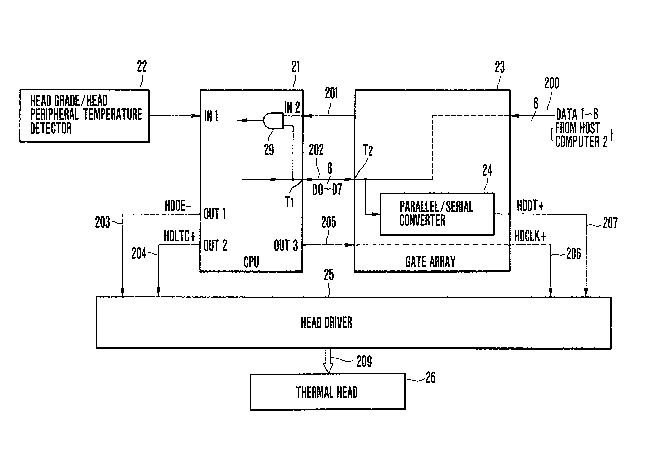
Referring to Fig. 2, a head grade/head periphcral
temperature detector 22 for detecting the grade of heat
accumulation of the head and the peripheral or ambient
temperature is connected to an input terminal IN1 of a CPU
21. A data reception interruption signal is supplied from
the host computer to an input te~minal IN2 of the CPU 21
through a line 201. An input/output terminal T1 of the CPU
21 and an input/output terminal T2 of a gate array 23 are
connected through a bidirectional data line 202. The input
terminal IN2 and the input/output terminal T1 in the CPU 21
are connected to the two input terminàls of an AND gate 29.
The output terminal of the AND gate 29 is connected to a
processing circuit, not shown, of the CPU 21.
Output terminals OUTl and OUT2 of the CPU 21 are
connected to a head driver 25 through corresponding lines
203 and 204. A head driver enable signal HDOE- and a head
driver latch signal HDLTC+ are output from the output
terminals OUT1 and OUT2, respectively. A clock signal for
the head driver 25 is output from an output terminal OUT3
to the gate array 23 through a line 205. This clock signal
is converted into a head driver clock signal HDCLK+ by the
gate array 23, and the signal HDCLK+ is supplied to the
head driver 25 through a line 20~.
The input/output terminal T2 of the gate array 23
is connected to the input terminal of the parallel/serial
converter 24. The parallel/serial converter 24 supplies
:.
-- 10 --
.
,
serial head data HDDT~ to the head driver 25 through a line
207.
The head driver 25 outputs the printing data to a
thermal head 26 throuqh a line 209.
Fig. 3 is a circuit diagram of the head driver
25.
The operations of the circuits shown in Figs. 2
and 3 will be described below.
Referring to Fig. 2, the gate array 23 which
receives data 1 to data 8 from the host computer 2 through
the line 200 sends the data reception interruption signal
to the CPU 21 through the line 201. The CPU 21 analy~es
the reception data and performs thermal history control.
The CPU 21 detects the ambient temperature of the head on
the basis of the head grade data from the head grade/head
peripheral temperature detector 22 and defines a pulse
width of the signal HDOE- supplied to the head driver 25.
The CP~ 21 sends parallel data D0 to D7 edited by history
control and the head driver clock signal to the gate array
23 through the corresponding lines 202 and 205. The gate
array 23 causes the parallel/serial converter 24 to convert
the parallel data into the serial data in synchronism with
the head driver clock signal and sends the signals HDDT+
and HDCLK+ to the head driver 25. Thereafter, the CPU 21
sends the enable signal HDOE- and the latch signal HDLTCt
to the head driver 25. The signa~ ~DDT+ sent ~rom the gate
array 23 to the head driver 25 is written in registers 38-l
', ~
.
. . ,
,
, ~ ' :
.:
9~1~
to 38-8 at the leading edge of the signal HDCLK~. The
contents of the shift registers 38-1 to 38-8 are latched by
latch circuits 37-1 to 37-~ at the leading edge of the
signal HDLTC~ supplied from the CPU 21. The data latched
by the latch circuits 37-1 to 37-8 are supplied as output
signals DOUTl to DOUT8 through AND gates 36-1 to 36-8 and
inverters 35--1 to 35-8 to energize the corresponding
heating resistor elements R.
Thermal history control will be described in
detail below.
Fig. 4 is a flow chart showing the operation of
history control.
Referring to Fig. ~, when the reception data
interruption from the host computer 2 is detected in step
Sl, the CPU 21 performs reception data processing and
editing using the CG font (S2). These operations are
repeated, and the CPU waits for a print instruction. When
a print instruction is detected in step S3, the two-step,
one-step previous printing data or information E0 and El,
and the current-step printing data or information E2 are
set by a motor interruption, and the head position is set.
In step S5, the CPU 21 checks the factor of the print
interruption representing a print interruption. At first,
the print interruption is associated with the time interval
tl, and the flow advances to step S6. (ED0 + EDl)-ED2 is
calculated as the output data and is stored in a register
PD. The enable signal HDOE- is set at low level, and the
. ~
,
o~
printing time is initiated (Fig. 5(a)). The output data
(~ot 1) in the register PD i5 sent to the head driver 25
(S11).
The signal HDLTC~ i5 set at "H" level, and this
data is sent to the head 26 (S12). Thereafter, the signal
HDLTC+ is set at "L" level (S13). Information is printed
by the head. The CPU 21 checks in step S14 whether a print
interruption 1 is completed. Since YES in step S14, the
flow returns to step S5. A print interruption 2 associated
with the time interval t2 is generated. In step S7,
EDl-ED2 is calculated, and the calculated data is sent to
the head driver 25. The operations in steps Sll to S14 are
performed, and the print information is sent to the head 26
and printed thereby. The flow returns to step S15. A
print interrupt 3 associated with the time interval t3 is
input. In step S3, (ED0-EDlj-ED2 is calculated, and the
calculated data is sent to the head 26. The print
interrupt 4 associated with the time interval t4 is
generated, and data ED2 is sent to the head 26 and printed
thereby. One-dot line printing is completed. If YES in
step S14, the flow advances to step S15. The enable signal
HDOE- is set at "H'l level, and the flow advances to step
S16. The CPU 21 checks in step S16 whether printing of all
data is completed. If NO in step S16, the flow returns to
step S4, and the head positlon is changed in accordance
with a motor interruption. The above operations are then
- 13 -
- . -
,
. . ,
.
, .
,
~l~8~90~
repeated. When printing of all data is completed, the flow
returns to step S1.
Figs. 5(a) to 5(h) are timing charts showing
timings of the signals when the third dot line in Table 4
is to be printed.
The output signals DOUT1 to DOUT4 (Figs. 5(e) to
5(h)) supplied from the head drive:r 25 to the head 26 to
control the ON/OFF operation of the heating xesistor
elements R can have different levels during the time
intervals tl to t4 even while the enable signal HDOE- is
kept at "L" level (in the prior art, these levels are the
same when the enable signal level is kept at a
predetermined level).
In the printing control system for a thermal
printer according to the present invention as described
above~ the printing densities of the respective heating
resistor elements can be controlled on the basis of the
respective heat accumulation. Therefore, a nonuniform
density distribution can be greatly improved.
- 14 -
,: - -
.
. - . . : -
.: .. ~ . '~ :
., ., ,, : . . - . : ,
:. . - , ~ ' ~ .
' ,. ' , ' ' ', ' ' ' ' '