Note : Les descriptions sont présentées dans la langue officielle dans laquelle elles ont été soumises.
1;2 ~371~3
--1--
HIGH FREQUENCY ARC STABILIZER
Field of the Invention
_
The invention pertains to apparatus and
methods for stabilizing welding arcs. More
j 5 particularly, the invention pertains to methods and
j apparatus usable in connection with AC or DC tig
- welding devices to maintain continuity of the welding
arc during oscillations of the output voltage or
while initiating the arc.
Background of the Invention
Both AC and DC tungsten-inert gas (tig)
welding devices are generally known in the art. In
such devices, a hollow housing is provided wlth a
tungsten electrode positioned therein. An inert gas
;5 such as argon is expelled under pressure fro~ the
t.~ open front end of the housing. The inert gas
_ surrounds the tungsten electrode as well as the
region of metal to be welded.
It has also been known, with respect to tig
~20 welding, that it is necessary to supply a high
_voltage, on the order of 3500 volts or so to break
down the gas and start the arc. Conventionally, a
spark gap oscillator has been used in the prior art
~~for this purpose. The spark gap oscillator will
_~25 generate a 3500 volt, relatively high freguency,
'output signal which can be used to ionize the inert
gas and-thereby start the arc.
Conventionally, in prior art systems, the
spark gap oscillator has been powered by 60 ~z line
~!30 voltage through a step-up transformer to generate a
60 Hz high voltage input signal, on the order of 3500
!volts, whiah is then used to power the spark gap
oscillator. However, the same 60 Hz signals are also
used to provide output voltage and current to the
tungsten electrode and the metal members being welded.
~ 7 ~
As a result, the high voltage input to the
- spark gap oscillator can be in phase with the welder
output voltage and current.
In addition to being used to initiate the
arc, in AC tig welding equipment, the output of spar~
~- gap oscillator is critical to maintaining the ionized
condition of the inert gas during time intervals when
the output voltage is going through zero and changing
polarity. Without the high frequency signal from the
- 10 spark gap oscillator during these transition periods,
the arc will become extinguished.
-- ~owever, the input AC voltage has to exceed
- a predetermined threshold before the spark gap
~ oscillator receives a high enough voltage to result
f , in the air gaps breakins down to produce the desired
. oscillation. There is thus a dead zone when the
input AC voltage to the spark gap oscillator is below
this predetermined threshold. This dead zone will
occur during the same time intervals that the output
20 voltage is also crossing through zero, provided the
-~ voltage to the spark gap oscillator is in phase witb
~ the output voltage. ~ence, the time when the output
voltage should be receiving the high frequency signal
from the spark gap oscillator so as to maintain thé
25 inert gas in its ionized condition is exactly the
time when the spark gap oscillator will cease to
_ function.
~ To avoid this problem, it has been known
- generally to shift the phase between the output AC
30 voltage and the AC voltage input to the spark gap
oscillator. This solution has had some measure of
success. ~owever, ~ewer tig welding machines with
wave balance controls have varying points at which
the output voltage transitions through zero due to
35 the output current and the wave balance setting.
1~7~
--3--
In such machines a phase shifting circuit
does not solve the problem completely. Due to the
asymmetrical shape of the output wave form it may not
be possible to adjust the phase of the spark gap
oscillator input voltage so that the oscillator is
functioning at all times that output transitions
occur. Hence, the results of this solution tend to
be inadequate.
Thus, there continues to be a need to be
able to drive the spark gap oscillator so as to
minimize or completely eliminate dead zones in the
output thereof. Further, it would be desirable to be
able to not only incorporate such driving circuitry
into new machines but to be to able to retrofit
existing tig welding units so as to eliminate this
dead zone.
.~ .
,~,
712~
- 3a -
Summarv of the Invention
The invention provides an apparatus and method for high
frequency arc stabilization of a welder. The apparatus is usable
with a welder having a hiqh frequency spark gap generator.
In accordance with the present invention, the apparatus
includes means for generating a repetitive, non-synchronized,
electrical signal with at least two voltages of differing values
wherein transitions from one of the voltages occurs substantially
instantaneously. Additionally, means couples the non-
synchronized electrical signal to the high frequency spark gap
oscillator such that an essentially continuous high frequency
output signal is generated by the spark gap oscillator. When the
apparatus is used with existing and new tig welding units, the
tig welding arc is more stabilized.
The apparatus preferably includes a relatively high
frequency oscillator which is not synchronized to the alternating
current voltage used to power the welding equipment. This
oscillator is coupled through buffering circuits so as to form
two pulse trains, one inverted with respect to the other. The
two pulse trains are coupled through a high voltage step-up
transformer which generates a high voltage rectangular wave for
the purpose of driving the spark gap oscillator.
The essentially instantaneous transitions of the high
voltage rectangular wave used to drive the spark gap generator
result in essentially continuous high frequency output from that
oscillator.
,; .
"'~, .. .
' ' `' ~'
. ~. ,
~' ,
~ 2~3712~)
-- 4
The non-synchronized oscillator can be implemented with a
Schmitt trigger. The output from the oscillator can be passed
preferably through first and second Schmitt triggers with one of
the outputs being inverted, to provide two rectangular out-of-
phase driving signals. The driving signals can each be coupled
to a gate input of an MOS field effect transistor. The MOS field
effect transistors can in turn be coupled to the high voltage
step-up transformer which in turn drives the spark gap
oscillator.
Further, in accordance with the invention a method is
provided for stabilizing a tig welding arc. The method includes
the steps of: generating a repetitive, nonsynchronized
electrical signal with at least two voltages of differing values
with transitions from one voltage to the other voltage which
occur substantially instantaneously; and coupling this
nonsychronized electrical signal to a high frequency spark gap
oscillator which in turn will generate a essentially continuous
high frequency, high voltage output signal feasible to stabilize
the arc.
The invention also provides a system for gating the
out-of-phase driving signals. By gating the driving signals off
of selected power initiating pulses, the high voltage, high
frequency stabilizing signal can be limited to a few milliseconds
during which the output voltage is crossing through zero volts.
As a result, the welder control system is subjected to
substantially less electrical noise.
~..?~
12~3712-.~
- 4a -
Numerous other advantages and features of the present
invention will become readily apparent from the following
detailed description of the invention and the embodiments
thereof, from the claims and from the accompanying drawings in
which the details of the invention are fully and completely
disolosed as a part of this specification.
,.~
Description of the Drawings
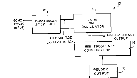
FIGURE I is a block diagram of a generally
known arc stabilizer system usable with a tig welder;
FIGURE 2 is a plot of sinusoidal high
voltage input to the arc stabilizer of Figure 1 and a
plot of the high frequency output of the spark gap
oscillator illustrating the presence of a dead zone;
FIGURE 3 is a block diagram of an arc
stabilizer in accordance withe present invention;
FIGURE 4 is a detailed electronic schematic
of an arc stabilizer in accordance with the present
invention;
FIGURE 5 illustrates driving voltages of the
circuitry of Figure 4 as a function of time;
FIGURE 6 is an electronic schematic of a
gating circuit usable with the arc stabilizer of
Figure 4; and
FIGURE 7 is a timing diagram illustrating
various waveforms found in the gating circuit of
Figure 6.
Detailed Description of the Preferred Embodiment
While this invention is susceptible of
embodiment in many different forms, there is shown in
the drawing and will be described herein in detail a
specific embodiment thereof with the understanding
that the present disclosure is to be considered as an
exemplification of the principles of the invention
and is not intended to limit the invention to the
specific embodiment illustrated.
Figure 1 illustrates a prior arc high
frequency arc stabilizer 10 of a type generally
known. The arc stabilizer 10 includes a step-up
~,~
: . '
~, ~2~3'71~
transformer 12 which transforms 60 ~z, 115 volts AC
input to 60 Hz, 3500 volt output. The high voltage
step-up transformer 12 provides eleGtrical input to a
spark gap oscillator 14 of a known type. The high
frequency output of the spark qap oscillator 14 is
coupled by a high frequency coupling coil 16 to the
welder output 18. The system 10 could be used with
AC or DC welders.
Figure 2 illustrates a sinusoidal high
10 voltage input to the spark gap oscillator 14 as a
function of time and high frequency output from the
spark gap oscillator 14. As can be seen from Figure
- 2, a dead zone exists when the input voltage falls
below predeterminable threshold values ET~, -ETH
15 as it approaches the zero volts periodically. This
-~ results in a dead zone in the high frequency, high
voltage output of the spark gap oscillator 14.
If a rectangular input wave is provided to
the spark gap oscillator 14, having essentially
- 20 instantaneous transitions between first and second
; voltage levels, the dead zone in the high frequency
output voltage can be essentially eliminated. The
block diagram of Figure 3 is an arc stabilizer system
- 20 which eliminates the dead zone in the high
25 fre~uency output of the spark gap oscillator 14.
~ The system 20 is illustratively powered off
u of 115 volts ~C, 60 Hz. The input alternating
current and voltage are rectified and filtered in a
. power supply 22. The power supply 22 powers an
30 astable oscillator 24.
~ The oscillator 24 can be implemented in a
variety of ways. The exact implementation of this
oscillator is not a limitation of the present
invention. The output signal of the oscillator 24
35 can be set to a variety of frequencies. One
~2~7~
frequency which has been found useful is 240 Rz. The
output freguency of the oscillator 24 is asynchronous
with respect to the input 60 ~z signal.
Buffer circuits 26 generate an asserted and
5 a negated rectangular signal on first and second
output lines 28 and 30, respectively. The drive
signals on the lines 28 and 30 provide input voltage
to the gates of switching transistors 32 and 34,
respectively. Preferably, the switching transistors
32 and 34 will be power MOS field-effect transistors
which display a high input impedance at each gate
input.
The field effect transistors 32 and 34
~ alternately drive the step-up transformer 12. Output
from the step-up transformer 12, a high voltage, high
; frequency wave then provides input to the spark gap
oscillator 14. Use of the system 20 results in the
spark gap oscillator 14 generating an essentially
continuous high voltage, high frequency output signal
_ 20 to the coupling coil 16.
Figure 4 is an electronic schematic of the
system 20. The power supply 22 includes a bridge
-~ rectifier 40 as well as filtering an output circuitry
~ 42. The free-running oscillator 24 can be
- 25 implemented with a single element 44 from a hex
- Schmitt trigger with an appropriate feedback loop
~ 46. In this case, the feedback loop 46 is a 33R ohm
- resistor.
The 240 ~z sguare wave output signal from
the oscillator 24 provides input to drivers 50 and
52. The resistor capacitor networks 54 and 56
-
coupled to the driver Schmitt triggers 50 and 52,
~ respectively, will be discussed subsequently. Output
from the driver 52 is inverted in a S_hmitt trigger
5B.
.. . . . . .. .
~Z~371;~
The rectangular wave forms on the lines 28
and 30 are thus essentially inverted with respect to
one another. Electrical signals on the lines 28 and
30 are coupled to the gate inputs of high power MOS
field effect transistors 32 and 34, respectively.
, The transistors 32 and 34 are in turn coupled to the
primary of the transformer 12.
The system 20 can be installed on new tig
welding eguipment and can be retrofitted onto
~ 10 existing tig welding equipment.
The function of the resistor-diode networks
54 and 56 is to insure that the transistor 32 is
~ completely turned off before the transistor 34 is
turned on. Figure S illustrates the effects of the
network 54 and 56. As can be seen, output on the
line 28 is slightly out of phase with output on the
! line 30. The respective transitions are shifted
approximately 20 microseconds with respect to one
another. This insures that both transistors are
turned off before an attempt is made to turn either
~ one of them on.
While the circuitry of Figure 4 above is
effective to generate the high frequency arc
; stabilizing signals usable to start a DC tig arc and
2S required for the continued ~.aintenance of the AC tig
; arc, the continuously present high frequency,~high
voltage output signals from the spark gap oscillator
- 14 can disrupt the welding system control circuitry.
In welders which utilize silicon controlled
rectifiers to switch the output current, a timing
network is very often used which is triggered by a
~ zero crossing detector. The zero crossing detector
=i detects when the main transformer secondary voltage
passes through zero. A selected interval of time
3S later, a timing circuit then generates an output
~2~'71X~3
pulse which is utilized as a gate input pulse for the
appropriate silicon controlled rectifier. However,
if the high frequency noise generated by the spark
gap generator 14 disrupts this process, incorrect
gate pulses can be generated which can cause
triggering of the silicon controlled rectifiers too
~ soon.
q It would be desirable to be able to gate the
system of Figure 4 such that the drive signals on the
lines 28 and 30, the gate inputs to the field effect
transistors 32 and 34 are only present for short
periods of time when the output AC voltage is
approaching a zero crossing. A schematic diagram for
a system 60 which provides such a gating function is
found in Figure 6.
~ Input to the system 60 comes from LM 555
- timer chip 62 which is found in existing tig welding
equipment. The chip 62 generates SCR gate drive
signals on a line 64 at appropriate time intervals in
response to input signals on a line 66.
~. The downgoing signal on the line 64 can be
- used to turn on a selected silicon controlled
rectifier. Output from the timer 62 on the line 64
can be used as input to a Schmitt trigger 66. The
~ 25 Schmitt trigger 66 inverts the signal on the line 64
and generates an output on a line 68. The positive
going ~ignal on the line 68 provides input drive to a
Schmitt trigger 70 via a resistor-diode-capacitor
network 72.
The effect of the network 72 is to stretch
the downgoing output pulse from the Schmitt trigger
~ 70. This pulse appears on a line 74. The downgoing
3 signal output on the line 74 is coupled via diodes to
lines 50A and 58A of Figure 4.
~ ql2() ~-~
--10--
The low or ground voltage on the line 74
permits the Schmitt triggers 50 and 58 to switch and
respond to the input 240 ~z signal from the
oscillator 24. Drive is then available for the field
effect transistors 32 and 34. This then results in
operation of the spark gap oscillator 14.
A high voltage on the line 74 will inhibit
switching of the Schmitt triggers 50 and ~8, thus
inhibiting drive to the field-effect t~ansistors 32
and 34. This blocks operation of the spark gap
oscillator 14.
The duration of the low voltage present on
the line 74 is set by the values in the network 72.
- The indicated values produce a 2 millisecond pulse
width on the line 74.
- In Figure 7, high frequency noise is
illustrated present on the line 66 during this 2
millisecond interval. This interval ends before the
signals on the line 66 increase in value to the point
_ 20 where false SCR gate triggering pulses can be
~ generated.
}n addition to generally reducing the noise
_ ~n the control system, the gating system 60 limits
~ the power required to drive the spark gap oscillator
14 since it only functions for approximately 2
,, ~ milliseconds during an 8 millisecond half period of
_ the 60 ~z output voltage. It will be understood that
- use of the Schmitt triggers 66 and 70 is purely
exemplary and 1~ not a l}mitation of the present
invention. Alternate forms of switching and
inverting circuitry could be used without departing
from the spirit and scope of the present invention.
~ From the foregoing, it will be observed that
numerous variations and modifications may be effected
; 35 without departing from the true spirit and scope of
.. , ~
~2~3712() -~
the novel concept of the invention. It is to be
understood that no limitation with respect to the
specific apparatus illustrated herein is intended or
should be inferred. It is, of course, intended to
~ S cover by the appended claims all such modifications
- as fall within the scope of the claims.
.
~ 15
-
... .
~ 20
c
_ 25
--
~ 30
-
3S
, . .. - . .. . ... ..