Note : Les descriptions sont présentées dans la langue officielle dans laquelle elles ont été soumises.
The present invention relates to a semiconductor
light emission device, and especially to a light emission
diode (hereinafter referred to as "LED") without an outside
attached lens and which can be produced by cnly a fine-
patterning process.
Semiconductor light emission devices generaily
comprise a semiconductor light emission element which is
constituted by epitaxial growth layers comprising, for
example, a p type indium-phosphorus (hereinafter referred
to as "p-InP") semiconductor substrate, a p-InP buffer
layer, a p type indium-gallium-arsenic-phosphorus (herein-
after referred to as "p-InGaAsP") semiconductor cladding
layer, a p-InGaAsP active layer,an n-InGaAsP cladding layer,
an n type indium-gallium-arsenic ~hereinafter referred
to as "n-InGaAs") semiconductor contact layer, an insulating
layer, such as silicon dioxide (SiO2), and a pair of electrodes.
In such a semiconductor element, a light emission region
which conducts light emission is produced at the center
portion of the active layer. A spherical lens is provided
on the light emission element for collecting the light
therefrom.
In this prior art semiconductor light emission
device with such a construction, when a current is injected
thereinto from the electrodes, light is isotropically radiated
from the light emission region of the active layer, is
guided to the outside, and is collected by the spherical
lens attached to the substrate. In this semiconductor
light emission device the conductivity types of the substrate
and the various epitaxial layers and the energy band gap
thereof are selected such that a current is concentrated
on the light emission region, that the recombinations of
the electron hole pairs are concentrated at that region,
and that the light generated at tne regions from tne light
emission region to the spherical lens can sufficiently
penetrate those layers.
In this prior art semiconductor light emission
device, however, the problem ex-sts of fixing the spherical
~'
lens onto the substrate, usually by adhesive, wi.tho~lt ~oiling
portions other than the requi.red portion by the adhesive.
An object of the present invention i.s to provide
an improved semiconductor light emission device which can
be produced easily and avoids the above problem.
According to the present invention, there is provided
a semiconductor light emission device, comprising a semiconductor
light emi.ssion element and a light collec-tion multiple
diffraction ring for collecting the light emitted from
said semiconductor light emission element.
Embodiments of the invention will now be described,
by way of example, with reference to the accompanying drawings,
in which:
Figure l is a cross-sectional view of a prior art
semiconductor light emission device;
Figure 2 is a cross-sectional view of a semiconductor
light emission device in accordance wi.th a first embodi.ment
of the present i.nvention;
Figure 3 is a pl.an view of the light collection
multiple di:Efraction lens of the device of Figure 2;
Figure 4 is a cross-sectional view of a second
embodiment of semiconductor light emissi.on devi.ce; and
Figure 5 is a plan view of another example of light
collection multiple diffraction lens for the device of
Figure 2.
Referring now to the drawings, Figure 1 shows a prior art semi-
conductor light emi.ssion device including a semi.conductor light emission
element 1 which is constituted by epitaxial growth layers
comprising a p type indium-phosphorus (hereinafter referred
to as "p-InP") semiconductor substrate 2, a p-InP buffer
layer 3, a p type indium-gall.ium-arsenic-phosphorus ~herein-
after referred to as "p-InGaAsp") semiconductor cladding
layer 4, a p-InGaAsp active layer 5, an n-InGaAsp cladding
layer 6, an n type indium-gallium-arseni.c (herei.nafter
referred to as "n-InGaAs") semiconductor contact layer
7, an insulating layer 8 such as silicon dioxide (SiO2),
and electrodes 9 and 10. In such a semiconductor element
i ~!
~2871SS
1, a light emission region 11 which conducts light emission
is produced at the center portion of the active layer 5.
A spherical lens 12 for collecting the light from the semiconductor
light emission element 1 is fixed by adhesive 13 onto the
semiconductor light emission element 1.
In this prior art semiconductor light emission
device with such a construction, when a current is injected
thereinto from the electrodes 9 and 10, light is isotropically
radiated from the light emission region 11 of the active
layer 5, is guided to the outside, and is collected by
the spherical lens 12 attached to the substrate 2.
The conductivity types of the substrate 2 and the epitaxial
layer 3 to 7 and the energy band gap thereof are selected
such that a current is concentrated on the light emission
region 11, so that the recombinations of the electron hole
pairs are concentrated at that region, and the light generated
at the regions from the light emission region 11 to the
spherical lens 12 can sufficiently penetrate those layers.
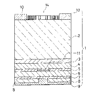
Figure 2 shows a first embodiment of the present
invention in which the same reference numerals are used
to designate the same or corresponding elements as those
used in Figure 1. The device includes a light collection
multiple diffraction ring 14 which is provided integrally
with the semiconductor light emission element 1, and effectively
functi~s as a lens utilizing the diffraction phenomenon
of the light. This multiple diffraction ring 14 may be produced
by growing a p-InGaAs epitaxial layer which has a narrower
energy band gap than that of the active layer 5 and which
does permit light penetration, and removing unrequired
portions by a fine-patterning process.
Referring now to Figure 3, the radius and the width
of each ring of the multiple diffraction ring 14 is determined
by the wavelength of the light to be generated and the
distances between the ring and the light source and between
the ring and the expected position at which the light is
to be collected. This can be produced by reduction of
1~8715S
the original drawing as in producing conventional mask
production, or by a method of approximate]y making a pattern
using a Newton ring which utilizes light interference.
This embodiment with a construction in which the
spherical lens 13 in the prior art device is replaced by
the light collection multiple diffraction ring 14, operates
similarly to the prior art device, because the multiple
diffraction ring 14 has a light collection ability equal
to that of the spherical lens 12. Furthermore, the device
requires no work or skill for fixing the lens because the
multiple diffraction ring 14 is produced by growing an
epitaxial layer on the rear surface of the semiconductor
substrate 2 of the semiconductor light emission element
1.
In the above-illustrated embodiment, the light
collection multiple diffraction ring 14 is provided integrally
with the semiconductor light emission element 1, but this
ring 14 may be produced on the main surface of a transparent
substrate 15 and fixed at a position apart from the semicon-
ductor light emission element 1~ as shown in Figure 4.
In the above-illustrated embodiment of Figures
2 and 3, the light collection multiple diffraction ring
14 is constituted by an epitaxial layer, but this ring
may also be formed of a metal which, provided at the rear
surface of the semiconductor substrate 2, also functions
as an electrode 10 of the semiconductor light emission
element 1. In this case, the production of the electrode
10 and the light collection multiple diffraction ring 14
can be conducted in a single process, thereby reducing
the production process. Moreover, the light collection
multiple diffraction ring 14 need not also function as
an electrode 10, but may be only required to be made of
the same metal as that of the electrode 10 for the purpose
of simplifying the production process. Fur-thermore, the
light collection multiple diffraction ring 14 may comprise
any other non-light transparent material than an epitaxial
layer or a metal. For example, the ring may be produced
,~
.. . . . ~ .. ~ .
~.X87155
by ion injecting impurities deeply into the semiconductor
substrate 2 so as to produce recombination centers of high
density in a multiple ring shape. As will be appreciated
by those skilled in the art, a ring formed by ion injection
will extend downwardly from the sllrface of the substrate
rather than project upwardly from it.
Furthermore, in the illustrated embodiment the
light collection multiple diffraction ring 14 is provided
at the rear surface of the semiconductor light emission
element 1, but the ring 14 may instead be provided at any
position because the light is irradiated isotropically from
the light emission region 11.
In the illustrated embodiment, the light
collection multiple diffraction ring 14 is produced so as
to have concentric circles the diameters of which can be
determined by calculation. However, even a ring having
circles deviating from the concentric and diameters
deviating from calculated values can be expected to exhibit
a light collection function of some degree depending on the
degree of the deviations.
In the illustrated embodiment, InP, InGaAsP,
InGaAs series semiconductor light emission devices are
described, but the present invention can be also applied to
GaAs or GaA As series semiconductor light emission devices.
Furthermore, it is desirable that the distance
between the light emission region 11 and the light
collection multiple diffraction ring 14 should be larger
than the limitation in the fine-pattern`ing process of the
multiple diffraction ring. The embodiment of Figure 4 is
advantageous from this point of view because the distance
can be freely selected.
As is evident from the foregoing description,
according to the present invention, a light collection
multiple diffraction ring is used instead of the spherical
lens of the prior art device, whereby the device can be
produced relatively easily by a fine-patterning process
without requiring skill.
C
~a~l~s
In the above-illustrated embodiment, the light
collection multiple dif~raction ring 14 is constituted
by an epitaxial layer, but this ring Inay be constituted
by a m~tal which, provided at the rear surface of the
semiconductor substrate 2, also functions as an
electrode lO of the semiconductor light emission
element l. In this case the production of the
electrode lO and the light collection multiple
diffraction ring l~ can be conducted at the same
process, thereby reducing the production process.
Besides, the light collection multiple diffraction ring
14 may not also function as an electrode 10, but may be
only required to be made of the same metal as that of
the electrode lO for the purpose of reducing the
production process. Furthermore, the light collection
multiple diffraction ring 14 may comprise any non-light
transparent material other than an epitaxial layer or a
metal. For example, the ring may be produced by ion
injecting impurities deeply into the semiconductor
substrate 2 so as to produce recombination centers of
high density in a multiple ring shape.
Furthermore, in the illustrated embodiment the
ligllt collection multiple diffraction ring 14 is
provide(l at the rear surface oE the semiconductor light
emissioll elelnent l, but ring 14 may be provided at any
~287155
-- 7
posltion because the ligllt is irradiated isotropically
Eroln the light emission region 11.
In the illustrated embodiment, the light
collection multiple diffraction ring 14 i3 produced to
5 have concentric circles whose diameters can be
determined by calculation, but even a ring having
circles deviated from concentric circles and diameters
deviated from calculated values is expected to have a
light collection function of some degree corresponding
to the degrees of the deviations.
In the illustrated embodiment InP, InGaAsP, InGaAs
series semiconductor light emission devices are
described, but the present invention can be also
applied to GaAs or GaA~As series semiconductor light
emission device
Furthermore, it is desirable that the distance
between the light emission region 11 and the light
collection multiple diffraction ring 14 should be
larger than the limitation in the fine-patterning
process of the multipLe diffraction ring. The
alteration of Figure 4 is advantageous in view of this
point because the distance can be freely selected.
As is evident ~rom the foregoing description,
according to the ;~.esent invention, a light collection
multiple diEEr=ctio~ ring is used instead oE the sphere
:
,,
:
. ~ -
1~87155
-- 8
lens of the prior art device, whereby the device can be
produced relatively easily by a fine-patterning process
without requiring no skill.