Note : Les descriptions sont présentées dans la langue officielle dans laquelle elles ont été soumises.
~L287383
NE-106
1 --
TITLE OF THE INVENTION
8-PHASE PHASE~SHIFT KEYING DEMODULATOR
BACKGROUND OF THE I~VENTION
. . . _
Field of the Invention
This invention relates generally to an 8-phase
Phase-Shift Keying (8 PSK) demodulator and more
specifically to such a demodulator featuring an improved
function by which resynchronization can be achieved in a
shorter time duration as compared with known 8 PSK
demodulators. This invention is highly suited for use in
a digital radio transmission system.
Description of the Prior Art
A digital radio transmission system is
susceptible to multipath fading or the like and invites
waveform distortion of the transmitted signal, which
degrades signal quality and which may cause a short break
in transmission reception. In order to minimize these
problems, it is the current practice to employ a
transversal equalizer using a transversal filter.
The transversal equalizer in a digital radio
transmission system, however, has encountered the
difficulty that distortion of the transmitted signal is
apt to exceed the equalizing capability thereof. More
specifically, upon the distortion reaching a level at
which the equalizer is unable to deal with same,
:
` ' ~ '
NE-106 1287383
asynchronism of clock and carrier signals in a
demodulator is induced and results in asynchronism of the
control loop of the transversal filter. These conditions
induce signal distortion within the equalizer itself.
Therefore, even if the distortion of the transmitted
signal again falls within the capability of the
equalizer, the synchronized state is not automatically
restored in the equalizer. A known approach to solving
this problem is to reset the tap gain signal generator
coupled to the transversal filter to its initial- state
upon the occurrence of asynchronism in the demodulator.
~f~oD r C~Q C ~>
C This prior art/malntains the equalizer at reset until
resynchronism of the clock and carrier in the demodulator
occurs. Accordingly, as the equalizer remains
inoperative during this time period, the control loop of
the equalizer is not brought into synchronization unless
the waveform distortion of the transmitted signal is
lowered to a considerable extent.
It is therefore highly desirable to have a
transversal equalizer restored to its normal state as
~x~ as possible upon the distortion of the transmitted
signal being reduced to a level at which the equalizer is
able to perorm its ~unction. To this end, intermittent
resetting o a transversal filter has been proposed in
the United States Patent No. 4,567,599 assigned to the
~ ~ -
- ; . '
:~2~73~33
NE-106
same entity as the instant invention. According to this
prior art, when asynchronism is detected .in a
demodulator, a reset signal is intermittently generated
to render the transversal filter operative at intervals
during a period in which the transversal filter is
paused. This prior art strives to shorten the
inoperative duration of the equalizer by discontinuously
checking quality recovery of an incoming IF signal
through intermittent resetting of the equalizer.
Howe~er, such a negative approach has proven insufficient
to effectively shorten the inoperative period of the
~: equalizer.
Further, no 8 PSK demodulator has yet been
proposed which i9 provided with the above-mentioned
function plus automatic gain control- for maintaining the
: incoming IF signal to a constant level.
SUMMARY OF THE I~VENTION
It is an object of this invention to provide an
8PSK demodulator equipped with a transversal equalizer,
which features an improved ~unction by which
resynchronization can be achieved in the minimun amount
of time.
It is another object to provide an 8 PS~
demodulator equipped with a transversal equalizer, which
is provided with improved resynchronization function plus
.~',
.
~:87383
7102~ 9
automatic gain control for maintaining an incoming IF siynal to a
constant level.
In general ~erms the present i~vention provides an 8-
phase phase-shift keyiny demodulator which features a rapid
resynchronization upon ~he demodulator goiny out of synchronism.
A plurality of error signals are produced wi-~hin the demodulator,
which error signals are used to determine whether a signa]. point
of an incoming 8-phase phase modulated siynal is usable for
conkroll:lng a transversal filter. An asynchronism signal, which
indicates whether the demodulator is synchronized, is derived ~rom
the demodulator and being applied to a kap gain control signal
generator coupled to the transversal filter. The tap gain control
signal generator is controlled when the asynchronism signal
; indicates asynchronism of the demodulator.
~ ore specifically, the present invention takes the form
of an 8-phase phase-shift keying demodula~or comprising: a
transversal equalizer for equalizing an incoming 8-phase phase `-
modulated signal, said transversal equalizer including a
; transversal filter and a tap gain contxol signal generator coupled
to said transversal filter; first means coupled to said
transversal filter and coherently demodulating the e~ualized
siynal; s~cond means, coupled to outputs of said first means, for
generéltlng a plurallty of error slgnals; third means for recelving
said plurality of error signals and dekermining whether a signal
point of said 8-phase phase modulated signal is usable ior
controlliny sald transversal equalizer, said third means producing
a first output; fourth means for detectinq asynchronism of said
. 4
;, ~...,...~,
w . ~
.
~Z~731~33
71024-69
demodulator, said fourth means applying a second output to said
tap ~ain control signal generator; and fifth means intexposed
between said third means and said tap ga.in control signal
qeneratorr receiving said first ou~put and controlling a plurality
of selectors form.ing part of said tap gain control signal
generator when .~aid second output indicates asynchronism of the
demodulator.
BRIFF DESCRIPTION OE THE D~AWINGS
The features and advantages of the present invention
}O will become more clearly appreciated from the following
description taken in conjunction with the accompanying drawings ln
which like hlocks or signals are denoted by like reference
numerals and in which:
Fig. 1 is a block diagram showing a first embodiment of
this invention;
Fiy. 2(A) is a waveform of a demodulated signal before
full-wave rectification;
~ig. 2(B) is a waveform of a demodulated signal after
full-wave rectification;
Fig. 3 is a phase diagram of an incoming
,...... ;.. ^............................................................ .
'
NE-106 12~7383
-- 6 --
demodulated IF signal which depicts the operation of the
first embodiment;
Fig. 4 is a block diagram showing in detail part
of the arrangement shown in Fig. l;
Fig. 5 is a time chart for describing the
operation of the arrangement shown in Fig. 4;
Fig. 6 is a block diagram showing a second
embodiment of this invention;
Fig. 7 is a phase diagram of an incoming
demodulated IF signal depicting the operation of the
second embodiment;
Fig. 8 is a block diagram showing a detail of
p~rt of the arrangement shown in Fig. 6;
Fig. 9 is a time chart showing the relationship
between three signals utilized in the arrangement shown
in Fig. 8;
Fig. 10 is a phase diagram of an incoming
demodulated IF signal which illustrates the operation of
the second embodiment;
Figs. 11 and 12 are illustrations for describing
the operation of the second embodiment;
Fig. 13 i8 a block diagram forming part of the
arrangement shown in Fig. 6;
Fig. 14 is a block diagram showing a third
embodiment of this invention; and
., -' .
. ,
NE-106
-- 7
Figs. 15 and 16 are illustrations for describing
the operation of this invention.
DETAILED_DESCRIPTION OF THE
PREFERRED EMBODIMENTS
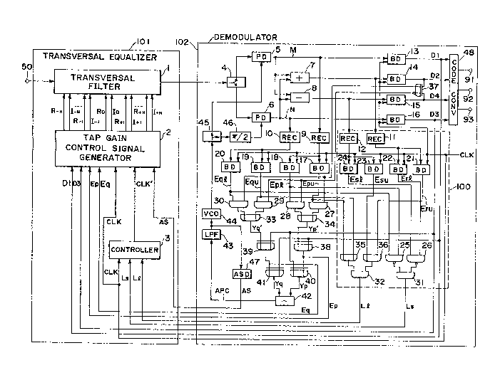
Reference is now made to Fig. :L, wherein a first
embodiment of this invention is shown in block diagram
form. The Fig. 1 embodiment features provision of three
blocks 3, 47 and 100 in a known 8 PSK demodulator
disclosed in ~K~ United States Patent No. 4,540,948
assigned to the same entity as the instant application.
Before discussing the first embodiment in detail,
an 8 PSK demodulator to which this invention is
applicable will first be described.
In Fig. 1, an 8-phase phase-modulated IF
(Intermediate Frequency) signal is applied via an input
terminal-50 to a transversal filter 1 which forms part of
a transversal equalizer 101. The equalizer 101 further
includes a tap gain control- signal generator 2 and a
controller 3. The transversal- equal-izer is provided to
prevent the degradation of signal quality by eliminating
intersymbol interference caused by the variations of
channel transmission characteristics due to fading, for
example.
The transversal filter 1 includes a tapped delay
line tnot shown) which is a~sumed to have (2N+l) taps in
NE-106 lZ87383
-- 8 --
this case (N = a positive integer). The output of each
tap is weighted by a variable gain factor in response to
the corresponding control- signal R_N, ..., Ko~ ..., R+
-N~ -~ Io~ -- or I~N- These control- signals are
supplied from the tap gain control signal generator 2.
The transversal equalizer 101 supplies its output
to two phase detectors (PD) 5 and 6 via a signal
distributer or splitter 4. A voltage-controlled
oscill-ator (VCO) 44 applies its output to the phase
detectors 5 and 6 by way of a signal distributer 45,
wherein the input to the phase detector 6 has been phase
shifted in a phase shifter 46 by ~/2 radians. The IF
signal-from the transversaI equalizer 101 is coherently
or synchronously demodulated by the phase detectors 5 and
6, which respectively apply their outputs (viz., baseband
signals M and N) to binary decision circuits (BD) 13 and
16 and further to an adder 7 and a subtracter 8. The
outputs of the adder 7 and the substracter 8 are fed to
binary decision circuits 14, 15, respectively. Note that
the outputs o~ the adder 7 and the subtracter 8 are
advanced in phase by ~r/4 and 3Tr/4 relative to the output
o~ the phase detector 5. ~he binary deci.sion circuits }3
through 16 respectively generate data signals Dl, D2, D4
and D3 which are fed to a code converter 48. The
~S converter 48 produces three channel data on its three
:
NE-106
:~287383
g
output terminals 91, 92 and 93 in a manner well known in
the art.
In order to control both VCO 44 and transversal
filter 1, the outputs of the phase detectors 5, 6/ the
adder 7, the subtracter 8, and the binary decision
circuits 13 through 16 are utilized.
The demodulated baseband signal M rom the phase
detector 5 is fed to a ful1--wave rectifier 9. This
rectifier 9 supplies its output to two binary decision
1~ circuits 17 and 18, which produce respectively error
: signals Epu and Ep. Similarly, the demodulated baseband
: signal N from the phase detector 6 is fed to a full-wave
rectifier 10. This rectifier 10 supplies its output to
: binary decision circuits 19 and 20, which produce error
. 15 signals Equ and EqQ, respectively. The binary decision
circuits 14 and 15 applies their outputs to an
Exclusive-OR gate 37 which applies its inverted output to
AND gates 28, 29, and its non-inverted output to A~D
gates 27, 30. The four error signals Epu, EpQ, Equ and
E~Q are ~ed to the AND gates 27, 28, 29 and 30,
respectively. An OR gate 33 receives the outputs of the
AND gates 29, 30 and supplies its output Yq' to an
Exclusive-OR gate 39. ~his gate 39 further receives the
data signal-D3 and produces an error signal Eq.
L1kewise, an OR gate 34 receives the outputs of th- ~3D
~`
- ,
:,''
NE-106 ~Z~73~
-- 10 --
gates 27, 28 and supplies its output Yp' to another
Exclusive-OR gate 38. This gate 38 is further supplied
with the data signal Dl and produces an error signal Ep.
The Exclusive-OR gates 40 and 41 respectively produce
signals Yp and Yq, which are applied to a subtracter 42.
The output of the subtracter 42 is applied via a low-pass
Eilter (LPF~ 43 to the VCO 44 as an automatic phase
control (APC) signal, and allows the VCO 44 to recover a
carrier wave. The above-mentioned control route is
referred to as an APC loop. In the above, application of
a cl-ock signal C~K has not been described for simplicity.
The tap control signal generator 2 is supplied
with the error signals Ep, E~ and the data signals Dl, D3
and a cl-ock signal (in the case of the prior art),
generating a plurality of tap gain control signals R ~,
o, ..., R+N, I_N, ..., Io~ .. and I~N. The
transversal-filter 1 receives these tap gain control
signals and minimizes intersymbol-interference.
The Fig. 1 blocks hitherto described are
disclosed in the aforesaid United States Patent No.
4,540,948 and hence further description thereof will not
be given for brevity.
As shown in Fig. 1, an asynchronism detector 47
is interposed between the low pass ~ilter ~LPF) 43 and
the tap gain control signal generator 2. This detector
NE-106 lZ~738~
-- 11 --
47 detects the impedance variation of the APC loop, and
outputs an asynchronism signal AS which indicates if the
carrier wave is out of synchronism in the demodulator 102
or not.
The Fig. 1 arrangement further comprises an
effective region determination circuit 100, which
comprises two full-wave rectifiers 11, 12, four binary
decision circuits 21 through 24, two NAND gates 25, 26,
two OR gates 35, 36, and two AND gates 31, 32, which are
coupled as shown. The full-wave rectifier 11 is supplied
with the output of the adder 7, and applies its output to
the binary decisio~ circuits 21 and 22. Another
full~wave rectifier 12 receives the output of the
subtracter 8 and applies its output to the binary
decision circuits 23 and 24. The binary decision
circuits 21, 22, 23 and 24 generate error signals Eru,
Er~, Esu and EsQ, respectively. The NAND gate 25
receives the error signals ~pQ and EqQ, whil-e the NAND
gate 26 recei~es the error signals ErQ and Es D . The OR
gate 35 receives the error signals Epu and Equ, while the
OR gate 36 receives the error signals Eru and Esu. The
AND gate 31 is supplied with the outputs of the NAND
gates 25 and 26, and outputs a small level control signal
Ls. On the other hand, the AND gate 32 receives the
outputs of the OR gates 35 and 36, and outputs a large
NE-106 12873~3
- 12 -
l-evel control signal LQ. The small and large level-
control signals Ls and LQ are given by the following
logic equations:
Ls = (EpQ + EqQ) (ErQ + EsQ)
= (Ep~ EqQ) (ErQ EsQ) (1)
LQ - (Epu + Equ) (Eru + Esu) -- (2)
wherein and + denote ~ND and OR operations,
respectively. The control signals Ls and LQ are applied
to the controller 3. The control signals Ls and Ll will
be discussed in detail with reference to Fig. 3.
Reference is made to Fig. 2 which illustrates, in
part (A) and (B) thereof, waveforms of the demodulated
signal before and after being full-wave rectified at 9 to
12 (Fig. 1). Each demodulated baseband signal-, applied
to the full-wave.rectifiers 9 to 12, is a 4-value s.ignal
whose values are defined by four reference levels "a" r
"b", "c" and "d" and which has six regions (1), (2), (3),
(4), (5) and (6). On the other hand, each full-wave
rectified signal (2-val-ue signal) has two reference
levels "a"' and "b"' by which the error signàls Epu, Equ,
Eru, Esu, EpQ, EqQ/ ErQ and EsQ are specified at the
corresponding binary decision circuit. Aq shown, in part
(B) of Fig~ 2, regions I, II and III respectively
correspond to the groups of regions ~(1), (6)), ((2),(5))
and ((3~,(4)). The following table shows the
,
NE-106 lZ~7383
- 13 -
relationship between the eight error signals and the
logic values of the six regions (l) through (6) from
which the error signals are specified.
Table
rror Signal Epu, Equ EpQ, EqQ
\ Eru, Esu Er~, EsQ
Reglon ~
(2) 1 ~
~3) 0 0
~ (6) ~ ~ l ~
It shoul-d be noted that each full-wave rectifier ~9, lO,
11 or 12~ of the first embodiment is AC (Alternate
1-5 Current) coupl-ed to the corresponding binary decision
c.ircuit.
Fig. 3 is a phase diagram which shows signal
points of an incoming 8-phase phase modulated IF signal
and "effective regions". This term "effective region" is
used throughout this specification in the sense as to
indicate a phase region wherein any slgnal poin~ shifted
thereto can be used to control the e~ualizer. The
xeference levels referred to in Fig. 2 are also added to
Fig. 3 to facilitate an understanding of how these
effective regions are defined. It will be understood to
NE-106
:~L2~3~38~1
- 14 ~
those skilled in the art that the effective regions of
the first embodiment are the non-hatched ones in view of
e~uations (1) and ~2) and the following description.
As shown in Fig. 3, four phases P, Q, R and S
define eight phase regions, and eight points A through H
represent normal points of an incoming IF signal. The
normal signal- points of. the IF signal are deviated or
shifted hy intersymbol interference. Let it he assumed
that the normal signal point ~ is shifted to a signal
point X, the point X is not suitable to produce the error
: and data signals according to which the equalizer is
controlled. This i5 because the point X is located
equidistant from the normal signal points A and B. In
other words, it can not be specified whether the deviated
: 15 signal point X belongs to the normal point A or B.
Accordingly, such a signal point should not be used to
produce the error and data signals for controlling the
equalizer. Generally, any point shifted into the hatched
regions must be neglected in terms of equalizer control.
On the other hand, assuming that the normal point
B is deviated to a point Y within a circle W and outside
the hatched region, the inormation khat the point Y is
within the eective region is provided by the small
level control signal Ls. It is reasonable to use such a
signal point for aontxolling khe e~ualizer in that it can
'
. ~ . . ..
'` '.
NE-106 ~287~3
be estimated with high probability that the signal- point
Y has been shifted from the nor~al point B. This can
also apply to the case that the normal signal point B is
shifted to a point Z l-ocated outside both the circl-e W
and the hatched region. The information that the signal
point Z is located within the effective region is
provided by the large level control signal L.
Fig~ 4 is a block diagram showing part of the tap
gain control signal generator 2 (viz.~ the portions for
1~ generating the tap control- signals R_l and Ro) and the
detail-ed arrangement of the control-ler 3, while Fig. ~ is
a timing chart showing the relationship between the
signals Ls, LQ, Yc and the cl-ock signal- CLK.
The tap gain control signal-generator 2 shown in
Fig. 4 comprises a correlato~ 71, two D flip-flops 75,
76, and two selectors 77, 78. On the other hand, the
controller 3 comprises an OR gate 72, an AND gate 73 and
a delay circuit 74. The signals Ls and LQ from the
effective region determining circuit 100 are applied to
the OR gate 72. The AND gate 73 receives the output of
the OR gate 72 and the clock signal- CLK, and applies its
output Yc to the delay circuit 74. The circuit 74
provides the applied signal-Yc with delay in order to
compensate for delay of the signals R~l', R0' provided by
the correlator 71, and applies its output (clock signal
NE-106 12873~3
- 16 -
CLK') to the clock terminals of the flip-flops 75, 76.
The correlator 71 receives the error signals Ep,
Eq, the data signals Dl, D3 and the cl-ock signal CLK, and
supplies its outputs R 1 " Rol to the data input
terminals D of the filp-fl-ops 75, 76, respectively. The
flip-flop 75 generates the signal-, which has been applied
to the data input terminal D, at the output terminal Q in
response to the clock signal CLK', and maintains its
state until the next cl-ock signal CLK' is applied
thereto. The other flip-~lop 76 functions similarly so
that the detailed description thereof will be omitted.
The sel-ectors 77, 78 are responsive to the signal AS
applied thereto, and select the outputs of the correlator
71 (R 1 " Rol) whil-e the signal AS indicates that:the
demodulator 102 is in synchronism, and, contrarily,
sel-ect the outputs of the flip-flops 75, 76 ~R-1", R0")
as long as the signal AS indicates that the demodulator
~ 102 is out of synchronism. The selectors 77, 78 apply
the outputs R 1' Ro to the transversal filter 1. In ~ig.
4, only two tap gain signals R 1' Ro are discussed.
~Iowever, as will be understood the above discussion is
also applicable to the remaining tap gain control
signals.
As will be understood ~rom the above, even if the
demodulator 102 is out of synchronism, the transversal
.
,
`
' . ,' ' ' ' ` '~'' ' ' :'
' ' '
' . ' ' '` ' : ,'
NE-106 ~28 7383
- 17 -
filter l is still controll-ed using the incoming IF signal
whose quality is determined to be useful for controlling
the transversal filter 1. This positive algorithm
accelerates the recovery of the normal- operation of the
transversal- equalizer, thereby effectively shortening the
divergent period of the equalizer.
Fig. 6 is a block diagram showing a second
embodiment of this invention. The difference between the
/Q ~te, r
~, first and second embodiments is that the ~e~4~
embodiment comprises an effective region aetermining
circuits 104 and a signal-level detector 105 in place of
the circuit 100 and further comprises an automatic input
l-evel controller 103. Other than this, the second
embodiment is e~ual in arrangement to the first one and
hence the description of the portions shared by both
embodiments wil-l be omitted. It shouLd be noted that
each full-wave rectifier (9 or 10) of the second
em~odiment is AC coupled to the corresponding binary
decision circuit, as in the first embodiment.
The effective region determining circuit 104
comprises two AND gates 58, 59, and an OR gate 61. The
AND gate 58 receives the error signals Epu, Eql, while
the AND gate 59 the error signals Equ, EpQ. The outputs
oE the AND gates 58, 59 are fed to the OR gate 61 which
generates a control signal Lm. The signal Lm indicates
NE-106 lZ~7383
- 18 -
whether or not each signal point of the incoming IF
signal is located within the effective region shown in
Fig. 7 by hatching. The control signal Lm satifies the
following l-ogic equation:
Lm = (Epu EqQ) + (Ep~ Equ) -- (3)
The control signal Lm is applied to the controller 3.
Fig. 7 is a phase diagram which shows the signal
points of the incoming 8-phase phase modulated IF signal
and the effective regions. The reference levels referred
l-0 to in connection with Fig. 2 are also added to Fig. 7 for
the ease of understanding how the effective regions of
this embodiment are defined. It shoul-d be noted that
effective regions of the second embodiment are the
hatched regions. How the effective regions are
determined wil-l be understood from equation (3).
In Fig. 7, the phases P, Q, R and S and the
normal signal- points A to H, have been referred to Fig.
3. For the same reason as in the first embodiment, the
signal point shifted to X cannot be used to produce the
error and data signals for controlling the equaliæer. On
the other hand, in the case where the signal point A is
deviated to a point Y within the effective regiont this
situation can be indicated by the control signal Lm. It
is reasonabLe to use the signal point Y for controlling
the equalizer in that it can be estimated with high
. - .~
. . .
NE-106
19
probability that the signal point Y belongs to the normal
point A.
Fig. 8 is a block diagram showing part of the tap
gain control signal generator 2 (viz., the portions for
generating the tap control signals R 1 and Ro) and the
detailed arrangement of the controller 3', while Fig. 9
is a timing chart of the signals Lm, Yc and the clock
signal CLK. Fig. 8 differs from Fig. 4 in that the
controller 3' of FigO 8 is not provided with the OR gate
72 and that the AND gate 73 receives the signal Lm and
the cloc~ CLK. Accordingly, in Fig. 9, there is no
waveform of the control signal-s Ls and LQ. The operation
of the Fig. 8 arrangement is similar to that of the Fig.
: 4 arrangement, so that further description thereof will
~e unnecessary.
The signal level detector 105 (Fig. 6) comprises
four inverters 51 to 54, three AND gates 55 to 57, and an
OR gate 60. The AND gate 55 receives the error signal-s
EpQ and EqQ, and the error signals Epu, Equ via the
inverters 51, 53, respectively. The AND gate 55 outputs
a small l-evel detecting signal Y~. The AND gate 56
receives khe error signal Equ, and the error signal- EpQ
via the inverter 52. The AND gate 57 receives the error
signal Epu, and the errar signal- EqQ via the inverter 54.
The OR gate 60 is supplied with the outputs of the AND
NE-106 ~73~3
- 20 -
gates 56, 57, and outputs a large level- detecting signal
YQ. The control signals Ys and Y2 are represented by the
following logic equations:
Ys = Epu Ep~ Equ Eql -- (4)
YQ = ~Ep~ Equ) + (Eq~ Epu) -- (5~
These signals Ys and Yl are fed to the automatic input
level controller 103 which comprises a variable gain
amp.lifier 91 and a variable gain amplifier controller 92.
Fig. 10 is a phase diagram showing the signal
points of the incoming IF signal, wherein the points
denoted by A through H are the normal signal points. in
the event that the amplitude characteristics of the
: transmission path or apparatus changes uniformly on the
: frequency axis, the distant of each signal point from the
: 15 origin O varies, accordingly. For example, the normal
signal point A shifts to a point A' when the gain in the
transmission path increases, while shifting to a point A'
when the gain in the transmission path is reduced. In
such a level shift, it may be difficult to produce
app.ropriate data and error signals from the demodulated
baseband signals. Therefore, it is necessary to control
the ampl.itude oE the demodulated signal to a constant or
strictly limited level irrespective of the varied
amplitude o~ the incoming IF signal.
Fig. 11 is a diagram showing location of the
-,
NE-106 lZ87383
- 21 -
signal points of the output of the ful1-wave rectifiers
(9, 10) which are AC coupled to the corresponding binary
decision circuit. The signal- points of the demodulated
signal (M, N), located in the second to fourth ~uadrants
(Fig. lO), are superimposed or folded to the flrst
quadrant when outputted from the binary decision circuit.
Accordingly, the signal points A, D, E and H of the
demodulated signal ~Fig. l~) are positioned at the signal
point A in ~ig. ll when outputted from the binary
decision circuit. Similarly, the signal points B, C, F
and G of the demodulated signal- ~Fig~ lO) are positioned
at the signal point B in Fig. ll when outputted from the
binary decision circuit. Likewise, (a) the signal- points
A', D', E' and H' each having a level higher than the
normal-l-evel, are positioned at a point J in Fig. ll, (b)
the signal- points B', C', F' and G' each al-so having a
level higher than the normal l-evel, are positioned at a
point K in Fig. ll, (c) the signal points A", D", E" and
H" each having a level lower than the normal l-evel, are
positioned at a point L in Fig. ll, and ~d) the signal
points B'l, C'l, F" and G~' each also having a level lower
than the normal level, are positioned at a point M in
Fig. ll, when outputted from the binary decision circuit.
It is understood that since each full~wave recti~ier ~9,
lO) is AC coupled to the corresponding binar~ decision
NE~106 1 ~ ~ 7383
- 22 -
circuit, the location of intermediate point V between the
points A and B does not change, and each signal point of
Fig. 10 is positioned on a line W according to the
ampl-itude thereof.
Accordingly, in order to maintain constant the
amplitude of the IF signal applied to the transversal
ilter 1, one of the large or small level detecting
signals Y~, Ys is outputted. More specifically, the
large level detecting signal Yl is generated when a
signal point falls within hatched regions shown in Fig.
12 (part (A)). On the other hand, the small 1-evel-
detecting signal Ys is ~enerated when a signal- polnt is
located in hatched regions shown in Fig. 12 (part (B)).
Reference is made to Fig. 13, which shows in
block diagram form the detailed arrangement of the
variable gain amplifier con~roller 92. The controller 92
comprises a J K flip-flop 81 which receives the signals
Ys and YQ and the clock signal CLK, and an averaging
circuit 82. As well-known, a J-K flip-flop outputs logic
"1" if clocked when logic "1" is applied to the J input
terminal, and outputs logic "0" if clocked wben logic "1"
is applied to the K input terminal. Accordingly, if the
large level detecting signal YQ assumes logic "1" ~viz.,
when large level is detected), the flip-flop 81 produces
~5 logic "0" at the output Q. Contrarily, if the small-
. .
''',
N~-106 ~73~3
- 23 -
level detecting signal Ys assumes logic "1" (viz., when
small-level is detected), the flip-flop 81 generates
logic "1" at the output Q. The averaging circuit 82 may
be an integrator for averaging the output of the
flip-flop 81. The output of the flip-flop ~1 is applied
to the variable gain amplifier of conventional type, and
controls the incoming IF signal so that its amplitucle is
maintained constant.
It is understood from the above that the second
embodiment features, in addition to the advantage of the
first embodiment, the automatic gain control by which the
amplitude of the IF signal-is maintained constant when
applied to the equalizer. Thus, the levels of the
demodulated baseband signal are maintained constant,
thereby el-iminating a short break or effectively reducing
the number thereof in transmission reception.
Fig. 14 is a block diagram showing a third
embodiment of this invention. The third embodiment is
essentially the same as the second one except that (a)
each ful-l-wave rectifier of the third embodiment is DC
(direct current) coupled to the corresponding binary
decision circuit and hence ~b) the arrangement of a
signal level detector 106 of the third embodiment i5
different from the counterpart lOS of the second
embodiment. Accordingly, the same portions of the second
~ ` .
NE-106
B73~3
- 24 -
and third embodiments will not be described.
The signal level detector 106 comprises four
inverters 51' to 54', four AND gates 63 to 66, and two OR
gates 67, 68. The AND gate 63 receives the error signals
Epu, EqQ via the inverters 51', 54', respectively, while
the AND gate 64 receives the error signals EpQ, Equ via
the inverters 52', 53'. Further, the AND gate 65
receives the error signals EpQ, Equ, while the AND gate
66 receives the error signals Eql, Equ. The OR gate 67
lD is supplied with the outputs of the AND gates 63, 64, and
generates a small level detecting signal Ys'. On the
other hand, another OR gate 68 receives the outputs of
the AND gates 65, 66, and generates a large level
detecting signal YQ'. The signal-s Ys' and Yl' are
represented by the following logic equations:
Ys' = ~Epu EqQ) + (EpQ Equ) ~ 6)
Yl' = ~EpU EqQ) + (EqQ ~ Equ) -~ (7)
The signals Ys' and YQ ' are fed to the automatic input
controller 103.
Fig. 15 is a diagram showing location of the
signal points of the output of the full-wave rectifiers
(9, 10) which are DC coupled to the corresponding binary
decision circuits, as mentioned above. ~he signal points
of the demoaulated signal ~M, N), located in the second
to fourth quadrants ~Fig. 10), are folded to the first
.
; '
: ' .
NE-106 12873~
- 25 -
quadrant when outputted from the binary decision circuit.
Accordingly, the signal- points A, D, E and H of the
demodulated signal (Fig. 10) are positioned at the signal-
point A in Fig. 15 when outputted from the binary
decision circuit. Similarly, the signal points B, C, F
and G of the demodulated signal ~Fig. lO) are positioned
at the signal point B in Fig. 15 when outputted from the
binary decision circuit. Likewise, (a) the signal points
Al, D', E' and H' each having a level higher than the
1~ normal level, are positioned at a point J in Fig. 15, (b)
the signal points B', C', Fl and Gl each also having a
level higher than the normal l-evel, are positioned at a
point K in Fig. 15, tc) the signal points A", D", E" and
H" each having a level-lower than the normal one, are
positioned at a point L in Fig. 15, and (d) the signal
points B", C", F" and G" each also having a level lower
than the normal level, are positioned at a point M in
Fig. 15, all- when outputted from the binary decision
circuit. I~ is understood that the signal- points A and B
moves respectively on the lines Wl and W2 when the levels
thereoE change. This arises from the above-mentioned DC
couple between the full-wave rectifiers (9, lO) and the
corresponding hinary decision circuit.
In order to maintain the amplitude of the
incoming IF signal to be constant, the large or small
.
.: , . ~ , .. .. . ~. . ~ , ,
NE-106 IZ87383
- ~6 -
level detecting signals YQ', Ys' is generated. More
specifically, the large signal detecting signal YQ' is
generated when a signal point falls within hatched
regions shown in Fig. 16 (part (A)). On the other hand,
the small-level detecting signal Ys' is generated when a
signal point is located in hatched regions shown in Fig.
16 (part (B)).
The foregoing description shows only a selected
number of embodiments of the present invention. The
various modifications possible without departing from the
scope of the present invention which is only limited by
the appended claims will- be apparent to those skilled in
the art.