Note : Les descriptions sont présentées dans la langue officielle dans laquelle elles ont été soumises.
~87g2~
CONTACT PIN
The invention relates to a contact pin for a printed circuit
board, in particular a contact pin comprising a compliant
portion for mounting the contact pin in a hole in the printed
circuit board~
U.S. patent 3,634,819 discloses a contact pin with a
compliant portion having two legs extending in the
longitudinal direction and joining a solid contact pln
portion at both ends. The legs are displaced outwardly in
opposite directions so that the legs are separated by a slot
along their whole length. During insertion the legs move
towards each other through the slot. Due to the slot the
cross section of the legs is decreased and thereby the
strength of the legs is decreased also.
U.S. patent 4,186,982 discloses a contact pin with a
compliant portion having two legs extending in the
longitudinal direction of the contact pin and joining a solid
contact pin portion at both ends. The legs are displaced
outwardly in opposite directions wherein the opposite
surfaces of the legs are partially overlapping each other
along their whole length. During insertion, the opposite
surfaces of the legs slide along~each other along their whole
lengrh thereby providing a sliding friction force to be
overcome during insertion resulting in a high insertion
force. This high insertion force may cause a cold weld
beeween the coating of the hole wall and the coating of the
compliant portion of the contact pin. Such a cold weld is
disadvantageous because~replacement of the contàct pin could
--1--
.. .. . . ..
~' '' ' . `' ' .. .
. . . :. -
,
- ' :: .'
. ' ', " '' , . . .
12~792~3
easily cause an unrepairable damage to the wall of the hole.
Moreover, as the diameter of the hole will vary during the
lifetlme of the printed circult board due to temperature
effects for example, this sliding friction force adversely
effects the long term retention force of the contact pin.
Furthermore, due to the frictional engagement of both legs or
spring members, the latter do not work independently from
each other resulting in an intermittently movement causing a
random spring ra~e. The asymmetrical configuration of the
compliant section is responsible for a torsion of the pin
ends after insertion, causing damage to the mating socket
contact. Although an anti-torsional feature can be built in,
as described in U.S. patent 4,186,982, it is very hard to
incorporate this in a miniaturized version (for small holes)
without loosing the elastic properties of both legs.
EP-A-0 141 492 discloses a contact pin with a compliant
portion having two legs arranged in the same manner as in US
patent 3,634,819. Further a center leg is provided in the
sloe between the two outer legs which center leg is displaced
radially outwardly in order to prevent torsion during
insertion. As in the contact pin of US patent 3,634,819, the
strength of the outer legs is decreased by the slot between
these legs. The center leg does not attribute to the
retention force in a significant manner.
The increasing integration of functions in IC's leads to a
demand for a higher number of connections on a printed
circuit board. Further it is desired to restrict the area
-2-
. ,
~792~
available for the contact pins 80 that more place will beavailable for the conductor tracks. Therefore it i8
desirable to use holes with a smaller diameter, for example
approximately half of the si~e of the currently used holes.
However, especially for small holes in a printed circuit
board, the flexibility of the compliant portion of the
contact pin has to be high in order to prevent damages to the
plating of the hole. Furthermore, sufficient spring strength
has to be foreseen in order to provide a sufficient retention
force.
With respect to a possible application of the prior art, U.S.
patent 3,634,819 and EP-A-0 141 492, for æmall holes (0.5 mm)
the cross-sectional area of the legs has to be further
decreased thereby limiting the springabilities and strength
of both legs to such an extent that unsufficient retention
force is obtained, whereby an electrical connection is not
guaranteed anymore during the lifetime of the system. In
view of the small dimensions of the contact pin suitable for
such small holes, the force required to overcome any possible
friction forces, as appearing in US patent 4,186,982, could
cause overstressing of the legs of the contact pin and
damages to the hole. It will be clear that overstressing of
the legs results in a low retention force.
It is a general object of the invention to provide a contact
pin adapted for use in small holes.
It is a further object of the invention to provide a contact
-3-
,, A .. ' . ' . , .; ~ ;
'~,~"'' ' ;' ;' '
.' . '.' . . . .
"' '
' i '-
" ~ ''
2~37~;~8
pin of the above-indicated type with an increased flexibility
in combination with a high strength of the legs.
It is a still further object of the invention to provide a
contact pin of this type with an improved long term retention
force by eliminating friction forces during insertion.
To this end the contact pin according to the invention is
characterized in that said legs are separated from each other
by a slot and in that each solid contact pin partion is
provided with a positioning element projecting from the
corresponding solid contact pin portion into said slot and
being displaced outwardly with respect to the solld contact
pin portions.
In this manner a contact pin is obtained with an increased
flexibility of the compliant portion and whereln during
insertion into a hole of a printed circuit board friction
forces will not occur, whereby the retention force is
guaranteed during the lifetime of the system. The
positioning elements provide an accurate positioning of the
contact pin in the hole before and after insertion.
Preferably said positioning elements are at least
substantially contacting the opposite surfaces of the legs in
the non-compliant parts thereof. Thereby, the strength of
the legs is improved.
The invention will be further explained by reference to the
drawings in which an embodiment of the contact pin of the
invention is shown.
--4--
:
: ' '
~ .
"' "`' '~ `'
,
~.28~79~3
Fig. 1 shows a front view of an embodiment of the contact pin
according to the invention.
Fig. 2 is a front view of the compliant portion of the
contact pin of Fig. 1 on a larger scale.
Fig. 3 is a side view of the compliant portion of the contact
pin of Fig. 1 on a larger scale.
Fig 4 is a cross section of the compliant portion of the
contact pin of Fig. 1.
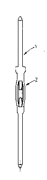
Referring to Fig. 1, there is shown a contact pin 1
comprising a compliant portion 2 for mounting the contact pin
in a hole of a printed circuit board not shown in the
drawing. Generally, the hole will be a so called plated
through hole provided with a lining of copper or the like
which is electrically connected with one or more conductive
circuit parts of the printed circuit board.
The compliant portion 2 should be designed in such a manner
that at each hole diameter within the tolerance range of hole
diameters on the one side a sufficient retaining force is
generated and on the other side the lining of the hole and
the surrounding area of the printed circuit board are not
severely damaged during insertion.
The compliant portion 2 of the contact pin 1 is shown in more
detail in Figs. 2, 3 and 4. The compliant portion 2
comprises two legs 3, 4 extending in the longitudinal
direction of the contact pin and joining a solid contact pin
--5--
..
~.;
1~79~:8
portion 5 at both ends. The solid contact pin portions 5
have a mainly rectangular cross sectlon wherein the corners
are rounded as indicated in Fig. 4.
The legs 3, 4 are separated from each other by a slot 6.
Each solid contact pin portion 5 is provided with a
positioning element 7, 8 projecting from the corresponding
solid contact pin portion 5 lnto said slot 6. Further the
positioning elements 7, 8 are displaced outwardly along
substantially their whole length with respect to the solid
contact pin portions 5. Each positioning element 7, 8 is
provided with a guidance surface 9 enclosing an angle of
approximately 45 with its outwardly directed surface.
As shown in the drawings, the legs 3, 4 are twisted into a
position in which these legs extend obliquely outwardly from
the positioning elements 7, 8. The positioning elements 7, 8
are at least substantially contacting the inwardly directed
suraces of the legs 3, 4 in the non-compliant parts thereof
joining the solid contact pin portions 5. In other words,
the width of the positioning elements 7, 8 is slightly less
than or at the utmost equal to the width of the slot 6 and
the length along which the positioning elements extend into
the slot 6 substantially corresponds wlth the length of the
non-compliant parts of the legs 3, 4. Thereby in the
embodiment shown in the drawings, the legs 3, 4 are initially
separated from the positioning elements 7, 8 and upon
insertion the legs 3, 4 will contact the positioning elements
with their non-compliant parts so that the legs 3,4 are
supported by the positioning elements.
~879~:8
Due to the slot 6 between the legs 3, 4 the compliant porcion
2 shows a high flexibility, wherein during insertion no
friction forces will occur. Thereby overstressing of the
legs 3, 4 and damageæ to the plating of the hole are
prevented and the long term retention force is not adversely
effected by friction. Since both legs 3, 4 or spring members
are acting independently, this design offers a predictable,
regular spring rate not disturbed by a random frictional
engagement.
The positioning elements 7, 8 provide an accurate positioning
of the contact pin in the hole and further favorably
attribute to the strength of the legs 3, 4. Further, the
positioning elements 7, 8 initialize in a favorable manner
the rotational movement of the legs 3, 4 during insertion.
By these features the contact pin 1 is especially adapted to
small plated through holes with a nominal diameter of + 0.5
mm.
The rotational movement of the legs 3, 4 guarantee an
accurate position of the ends of the contact pin 1 which will
not be pivoted out of their original positions by the
movement of the legs 3, 4. In this respect, reference is
made to EP-A-0 225 400 of the same applicant.
As shown in Fig. 3, the upper positioning element 7 opposite
of the end of the contact pin 1 to be inserted is provided
with a bevelled end face 10 at its free end. Thereby
--7--
'
,' ,.,'
J ~ ~37928
damaging of the wall of the hole by the positioning element 7
is prevented.
In the outwardly directed surfaces of the positioning
elements 7, 8 a groove-like recess 11 is provided acting as a
receiving space for any material scraped off of the wall of
the hole. Further the part of the positioning elements 7, 8
lying between the legs 3, 4 is bevelled at the sides facing
these legs. Thereby the torsion movement of the legs 3, 4 is
maximized.
It will be understood that the ends of the contact pin 1 can
be made in different manners depending on the application of
the pin. For example, the contact pin may be a socket
contact, and IDC-contact or an edge type contact.
The invention is not restricted to the above-described
embodiment which can be varied in a number of ways within the
scope of the claims.