Note : Les descriptions sont présentées dans la langue officielle dans laquelle elles ont été soumises.
3~
A SOLDER FIJOW WEI~ FOR REFLOWING SOLDER
OF MULTIPIN COMPONENTS
The present invention is directed to the field of
electronic component soldering and more specifically to
the area of reflowing solder to effect removal and
repair of multipin components.
The use of surface mounted devices (SMD's) on
printed circuit boards alongside microcomputers having
several parallel leads soldered into through-holes of
the printed circuit board have presented some difficul-
ties in the repair or removal of such microcomputer
components from the circuit boards. Generally, SMD's
are leadless resistors or capacitors that have end
terminals which are directly soldered to either surface
of a printed circuit board and, in many cases, are
located adjacent through-holes into which a multileaded
component is soldered. Accordingly, the reflow of an
entire area of a printed circuit board in order to
desolder the multileaded component would also cause the
desoldering and release of surface mounted devices
located on that surface. In such a case, when a new
multileaded component is installed to replace a defec-
tive component, the SMD'S that were removed during the
reflow process need to be replaced and thus add to the
c06t of the repair.
Several prior art patents relate to the problem of
removing integrated circuits from printed circuit boards
but do not attempt to overcome the problem noted above.
For inetance, U.S. Patent No. 4,270,260 utilizes
infrared lamps to bring the temperature of a printed
circuit board up high enough to reflow the solder in the
through-holes and allow removal of the integrated
circuit from the opposite side of the board.
U.S. Patent No. 4,659,002 describes a device in
which a masked area is defined to surround the solder
leads of an electrical component and solder is pumped
~k
~ "~8171
into the masked area in order to reflow the solder at
the concentrated area and allow removal of the
component.
U.S. Patent No. 3,557,430 also teaches the use of a
masking device which allows the concentration of solder
to provide reflow of soldered leads of an integrated
circuit mounted on a printed circuit board and the
removal thereof.
In each case, the prior art does not appear to be
concerned with the presence of SMD's or other devices
within the area outlined by the integrated circuit
through-hole pattern and, therefore, do not suggest a
solution to the problem.
In accordance with one aspect of the present
invention, there is provided a solder well for use in
the desoldering and removing of a multiterminal
electrical component from its soldered connection to a
printed circuit board. The solder flow well comprises a
closed outer wall having inner and outer surfaces that
are configured to have an upper edge that lies in a
generally horizontal plane. The well further includes a
closed inner wall having a first surface that opposes
the inner surface of the closed outer wall and defines a
molten solder receiving channel therebetween, that is
configured to have an upper surface that lies in a plane
generally coplanar with the upper edge of the closed
outer wall. The inner and outer walls define a channel
that corresponds to the pattern of the multipin terminal
connections to the printed circuit board. The channel
allows the entrance of molten solder to be concentrated
only in the area of the printed circuit board where the
leads of the multipin components are soldered. The heat
from the molten solder in the channel is thereby
concentrated to reflow the solder within that defined
area so as to not disturb the solder connections of
other components (especially SMD's) that are located on
381~71
the same side of the printed circuit board as the solder
reflow. The closed inner wall also has a second closed
surface that defines a cup to receive excess solder from
the channel and a means for draining the cup.
In accordance with a further aspect of the inven-
tion, there is provided a solder well for providing
molten solder to a defined level area that corresponds
to the through-hole pattern on a printed circuit board
to which a multipin component is soldered, comprising
means defining a channel for receiving molten solder to
the defined level area; means defining an inner cup for
receiving solder overflow from the channel means and
removing the solder overflow from the defined level
area; wherein the channel means surrounds the inner cup
means.
The invention is described further, by way of
illustration, with reference to the accompanying
drawings, in which:
Figure 1 is a top view of a multipin electronic
component, such as an integrated circuit, mounted on the
upper surface of a printed circuit board;
Figure 2 is a plan view of the bottom surface of
the printed circuit board corresponding to the area
shown in Figure 1 illustrating the through-hole pattern
into which the lead wires of the multipin component are
soldered;
Figure 3 is a perspective view of the solder well
invention described herein;
Figure 4 is a top view of the solder wall
invention shown in Figure 3; and
Figure 5 is an elevational cross-sectional view of
the solder well invention shown in Figure 3 as it is
applied to the printed circuit board shown in Figures 1
and 2.
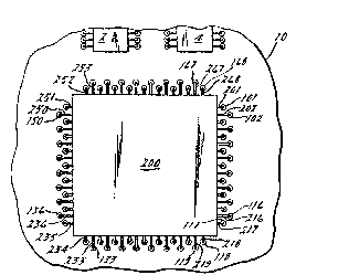
In Figure 1, a printed circuit board 10 of a
generally conventional insulative substrate i5 shown
8171
without details of the actual circuit pattern which is
conventionally placed on such printed circuit boards.
The top view of the printed circuit board 10, shown in
Figure 1, also depicts the location of integrated
circuits 2, 4 and 200. The integrated circuit 200 is
typical of a 68 pin microprocessor unit which is
utilized
~ ? ~17~
-- 4
in several products of assignee. (The actual content and
circuitry employed in the multipin component 200 is not
of concern in this invention and is not described in any
detail.) However as can be seen in Figures 1 and 2, the
68 pins 201-268 are soldered in through-holes 101-168 in
a pattern which corresponds to the location of the lead
wires extending from the multipin component 200. In the
case shown in Figures 1 and 2, the pattern forms a
rectangle.
In Figure 2, components 12, 14, 16, 18, 20, 22,
24, 26, 28 and 30 depict SMD's which are mounted on the
under side 100 of the printed circuit board 10 and are
located strategically within the printed circuit (not
shown) so as to have a functional effect on the circuit
and also allow for high density packaging of components
on a board. As described in the background section
above, the removal of defective multipin components 200
from the printed circuit board by utilizing conventional
methods would result in the desoldering of the SMD's
20 12-30, due to their location within the area defined by
the multipin components through-hole pattern.
The solder well 300, of the present invention
shown in Figures 3, 4 and 5, is a dual walled device in
which an outer wall 305 having an inner surface 306 is
25 disposed opposite an inner wall 308 having an outer
surface 307. The surfaces 306 and 307 of the outer and
inner walls 305 and 308 are separated to define a channel
having a width and length which corresponds to the
through-hole pattern into which the multipin component is
30 soldered on the printed circuit board 10. The outer and
inner walls 305 and 308 respectively contain edges 302
and 304, which further define coplanar surfaces that mate
with the printed circuit board and confine the channel to
that through-hole pattern.
3817~
The solder well contains inlets 310, 312, 314
and 316 within the channel to allow the inflow of molten
solder into the channel. A connector shroud 320 extends
below the solder well 300 so as to allow the solder well
to be press fitted into the aperture of a solder bath
retainer 400.
An inner cup area, defined by the inner wall 308
and a hase 323, contains drains 322, 324, 326 and 328
that allow excess solder that may overflow the channel to
escape away from the printed circuit board and thereby
avoid coming in contact with any area of the printed
circuit board that is outside the defined channel.
In operation, the printed circuit bOârd 10 is
placed over the solder well 300 so that the through-hole
pattern of the multipin component 200 is abutted and
continuously enclosed by the channel defined by the
parallel edge surfaces 302 and 304. The molten solder 30
is then pumped up from underneath the shroud 320 so that
it enters the channel through inlets 310, 312, 314 and
316 to a level wherein the convex meniscus 32 of the
solder 30 contacts the solder and lead wires of the
multipin component 200. Within a short period, the
solder joints in contact with the molten solder 30 are
cused to be reflowed. At such time, the multipin
component 200 may be easily removed and a new one placed
therein as a substitute. The printed circuit board 10 is
subsequently removed and the solder may be pumped down or
remain, if continually heated, so that the next device
for repair may be located over the solder well.
It will be apparent that many modifications and
variations may be implemented without departing from the
scope of the novel concept of this invention. Therefore,
it is intended by the appended claims to cover all such
modifications and variations which fall within the true
spirit and scope of the invention.