Note : Les descriptions sont présentées dans la langue officielle dans laquelle elles ont été soumises.
iZ~39217
1 PHOTODETECTOR HAVING CASCADED PHOTOELEMENTS
3 Fi~ld of the Invention
The present invention relates to photodetection means,
6 particularly photodetection means which reduces common mode
7 noise in output signals.
9 Discussion of the Prior Art
11 In magnetooptic recorders, the readback signals from record
12 media contain phase-rotated light polarizations representa-
13 tive of the recorded information. Such reflections contain
14 so-called "P" and "S" components. The P and S components
are typically separated for determining the polarization
16 rotation. Other forms of optical processing mav be employed
17 for separating the rotated-reflected polarized light so that
18 the light may be directed to one of two photodetectors. The
19 photodetectors in turn are respectively electrically con-
nected to transimpedance amplifiers or operational ampli-
21 fiers which in turn are connected to a differential ampli-
22 fier. The differential amplifier supplies a signal repre-
23 sentative of the difference in optical intensities impinging
24 upon the respective photodetectors for indicating which
direction the reflected light from the magnetooptic medium
26 has had its polarization rotated. The requirement of
27 separate transimpedance amplifiers for the respective
28 photoconductors results in electrical signal nois~ induced
29 into the readback signal. Further, four connections are
required for the photodetectors. Two for the respective
TU987007 1
,
~2~39217
1 transimpedance amplifiers and two for the electrical signal
2 bias. A problem also arises in that the transimpedance
3 amplifiers interposed between the respective photodetectors
4 and the inputs to the differential amplifier are not always
equal. As a result, common mode noise is induced into the
6 readback signal by the transimpedance amplifiers. Accord-
7 ingly, it is desired to replace the electrical connections
8 such that the common mode noise can be more efficiently
9 handled without requiring extensive electrical feedback
connections.
11
12 TYpically, a pair of photodetectors are connected to a
13 differential amplifier either directly or through trans-
14 impedance amplifiers. For example, U. S. Patent 4,589,102
shows photodetectors 10 and 12 connected to differential
16 amplifier 19. The anodes of the photodiodes 10 and 12 are
17 connected to the inputs of the amplifier. In a similar
18 manner, in U. S. Patent 4,580,255 in Figs. 14 and 16, a pair
19 of photodiodes 4-2 and 4-3 are respectively coupled to a
differential amplifier 4-4 through intervening operation
21 amplifier 21 and 22. This circuit arrangement is typical in
22 a magnetooptic recorder, even though the patent 4,580,255 is
23 not directed to~that end. Fig. 4 of U. S. Patent 4,566,088
24 shows two independent connections to amplifiers 120 and 120
in its Fig. 4. Again, the separate electrical connections
26 are subject to common mode noise insertion. Also U.S. Patent
27 4,446,545 shows three photodetectors 10 through 12 (Fig. 1)
28 with the photodetector 11 and 12 being individually con-
29 nected to separate inputs of circuit means which analyze the
relative light intensities of the two photodetectors. See
TU987007 2
l2as2~7
1 Fig. 6 of this patent. Again, co~mon mode noi~e is possibly
2 inserted by the electrical circuit means shown in this
3 patent. U. S. Patent 4,581,728 shows two photodiodes 33 and
4 31 receiving light from an optical system. The electrical
connections from the two diodes are through transimpedance
6 amplifiers 41 and 42 eventually to differential amplifier
7 50. Again, common mode noise can be introduced into such a
8 circuit arrangement.
U. S. Patent 4,578,786 is cited for its showing of the
11 photodiodes in Fig. 8 which are respectively connected to
12 differential amplifiers 220 and 222 for feeding into differ-
13 ential amplifier 226. Again, common mode noise is possible
14 with this arrangement.
16 U. S. Patent 4,563,760 is cited for its showing in Fig. 8
17 which shows diodes Dl and D2, not photodiodes, for providing
18 filtering action in an electrical circuit. There is no
19 function of cancellation of common mode noise in this
particular circuit arrangement.
21
22 Summary of the Invention
i~ 23
24 It is an object of the invention to provide electrical
apparatus of the photodetection type which can reduce or
26 eliminate common mode noise. In accordance with the inven-
27 tion, first and second photodetectors each having an anode
28 and a cathode have the cathode of one of the photodetectors
29 connected to the anode of the second photodetector. The
other connections to the photodetectors are for hiasing the
TU987007 ~ 3
12892~7
1 operation of the photodetectors. Output circuit means has
2 an input electricallv connected to the anode of the first
3 photodetector and the cathode of the second photodetector
4 for supplving an output signal having minimal common mode
noise. It is preferred that the photodetectors have identi-
6 cal electrical and physical properties for minimizing common
7 mode noise. It is also preferred that the photodetectors be
8 of the diode type.
In another aspect of the invention, the photodetector is
11 formed on a single, semiconductor chip with an isolation
12 zone between the photodetectors and circuit means used to
13 process output signals based upon the photo-induced opera-
14 tion of the two photodetectors. In one embodiment, the
isolation zone is about five mils such that an isolated
16 region containing the two photodetectors is physically
17 separated from the isolated region containing the ampli-
18 fiers.
19
The circuits and arrangements of the present invention are
~; 21 most advantageously employed in an optical signal recorder
22 and playback system.
~,,,
23
24 The foregoing and other objects, features, and advantages of
the invention will be apparent from the following more
26 particular description of preferred embodiments of the
, . ~. .
27 invention, as illustrated in the accompanying drawings.
28
29
~ .
~ TU987007 4
`
12892~7
1 Description of the Drawinqs
3 Fig. 1 is a simplified circuit schematic showing the opera-
4 tion of the present invention.
s
6 Fig. 2 is a aiagrammatic showing of a single semiconductor
7 chip incorporating the Fig. l-illustrated circuit.
9 Fig. 3 is a greatly simplified showing of an optical record-
er capable of using the Fig. l-illustrated circuit arrange-
11 ment.
12
13 Detailed Description
14
Referring now more particularly to the drawings, like
16 numerals indi~ate like parts and structural features in the
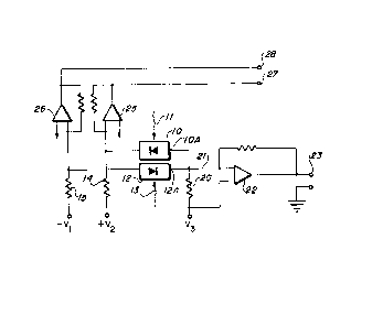
17 three figures. In Fig. 1, a pair of photodetectors 10 and
18 1~, shown as photodiodes, are arranged to respectively
19 receive light beams 11 and 13. Photodiodes 10 and 12 may
be, and preferably are, formed on a single semiconductor
21 chip such that the electrical and physical properties of the
22 two photodiodes are as closely together as possible. It is
23 to be understood that phototransistors and other photo-
24 detection elements may bë readily substituted for the
photodiodes 10 and 12. The terms "anode" and "cathode" as
26 used with respect to the photodiodes lO and 12 for photo-
27 transistors respectively refer to the collector and emitter,
28 as well as to comparable element portions of other photo-
29 elements which may be successfully employed in the Fig. 1
illustrated circuit. The anode lOA and the cathodq 12A
TU987007 ~ 5
- 1289~;7
l respectively of photodiodes 10 and 12 are ohmically con-
2 nected together as by a low-impedance ~lectrical lead. Thi~
3 electrical connection provides a signal output connection of
4 the two photodiodes 10 and 12. The second connection is to
a reference potential as is known for electrical circuits.
6 The cathode portion of photodiode 10 is connected to a first
7 electrical bias source 14 connected to a bias potential +V2.
8 The anode of photodiode 12 is ohmically-electrically con-
9 nected to bias source 15 which in turn is connected to
biased voltage -Vl. In this situation, the photod~iodes lO
11 and 12 are reversed biased with the impinging light beams 11
12 and 13 causing the electrical current conduction in the
13 circuit formed between the photodiodes and the electrical
14 bias circuits.
16 The anode lOA and cathode 12A are suitablv coupled to a bias
17 circuit 20 which has a bias voltage V3. Electrical lead 21
18 is an input portion of output circuit means 22 which com-
19 prises a typical transimpedance amplifier for converting the
electrical current flowing between the photodiodes 10 and 12
21 to an electrical voltage signal at output terminal 23.
22 Characteristic of the electrical signal is the complete
23 elimination of common mode noise when the photodiodes 10 and
i; ~ 24 ~12 are electrically and physically identical, preferably on
,
a single semiconductor chip.
26
,
27 The signal on output terminal 23 is representative of a
28 difference signal of light intensities respectively imping-
29 ing upon photodetectors 10 and 12. Accordingly, the circuit
arrangement is a simple substitution for the prior art which
TU987007 6
~289217
1 required two transimpedance amplifiers to be electrically
2 interposed respectively between two photodetectors and a
3 differential amplifier. ~ence, the function is performed
4 with two less amplifier circuitfi and fewer connections to be
made in either a semiconductor chip or a circuit board.
6 Electrical noise is reduced in that a single transimpedance
7 amplifier constituting output circuit means 22 replaces the
8 concatenated connection of a transimpedance amplifier with a
g differential amplifier in the prior art. Such elimination
of circuit means results in a signal-to-noise improvement of
11 about 3 db (decibels).
12
13 The individual light intensities in impinging upon photo-
14 detectors 10 and 12 can also be measur~d from the Fig. 1
illustrated circuit. A pair of operational transimpedance
16 amplifiers 25, 26 are respectively connected to the cathode
17 of the first photodetector diode 10 and the anode of the
18 second photodetector diode 12. The two operational amplifi-
19 ers 25, 26 respectively supply the output electrical signals
to terminals 27 and 28 which may be used for indicating
21 tracking error signals in optical disk recorders whereas
22 terminal 23 may be used for indicating either focus errors
., ~ .
23 or for indicating data, depending upon the optical and
~24 physical arrangements of the optical data recorder player in
which the circuit is used. The electrical bias circuit
26 means 14 and 15 may be incorporated into the àmplifiers
`~ 27 25,26 rather than being separate as shown in Fig. 1.
~ 28
- 29 Fig. 2 illustrates a single chip embodiment of the Fig. 1
photodetection system. Placing all of the circuit
TU987007 7
12892~7
1 components on a single chip reduces cost, makes a smaller
2 photodetection circuit and thereby allows a smaller photo-
3 detection head to be constructed such as shown in Fig. 3.
4 The chip 30 includes two isolated semiconductor regions 31
and 32 which are separated about five mils (0.005 inches) by
6 isolation zone 33. The photodiodes 10 and 12 are suitably
7 formed within the first isolated re~ion 31 whereas the
8 amplifiers 22, 25 and 26 are suitably formed in the second
9 isolation region 32. Suitable electrical connections can be
mad~ on the semiconductor chip 30 using known technology and
11 following the circuit arrangement shown in Fig. 1.
12
13 Fig. 3 is an extremely simplified drawing of an optical disk
14 readback system which includes a magnetooptic or other
optical medium 50 being scanned by an optic system 51 of
16 known design, and hence not detailed. A laser supplies
17 light over light path 52 to optics 51 which in turn directs
18 the received laser light beam to medium 50 via two-way light
19 path 53. The light reflected from optical medium 50 tra-
verses path 53 into optics 51. Optics 51 in a known manner
; 21 direct the reflected light to the photo section 54 which
22 includes photodiodes 11 and 12 and the semiconductor cir-
~23 cuits comprising the electrical connections of Fig. 1 and
:,. . .
24 the amplifiers 22, 25 and 26. Photo section 54 is prefer-
ably bonded and optically secured to the optics 51 which in
, . ~
~ 26 turn constitute a plurality of optical prisms and the like
-- ~
~ 27 suitably bonded together, using known techniques. Output
.
28 terminals 23, 27 and 28 lead from photo section 54 ta detec-
29 tion and control circuits, as is known in the art.
TU987007 8
~ .
1289P~
l While the invention has been particularly shown and de-
2 scribed with reference to preferred embodiments thereof, it
3 will be understood by those skilled in the art that various
4 changes in form and details may be made therein without
departing from the spirit and scope of the invention.
11
12
13
14
~16
17
18
19
:: ~
~21
22
.,~, . ,
23
24
~25
:~26
.
,~:
:~: 27
,
~28
; 29
~: 30
,
TU987007 . 9
~ -